As part of this week, our group worked together on the output devices group assignment — measuring the power consumption of different output devices to understand how much current and power each actuator draws, then documenting our shared findings before our individual projects. You can read the complete group assignment, including the measurements and our shared documentation, here:
Group AssignmentGroup Assignment
Project Overview
Output Device
For this week I worked with an output device by controlling a heating element using an ESP32. The purpose of this assignment was to understand how a microcontroller can switch a high-power load and regulate a physical variable — in this case, temperature — in a closed loop.
A heater is a particularly interesting output device because, unlike an LED or a servo, it cannot be switched at logic-level current directly from a GPIO pin. It requires a driver stage (a MOSFET) and, more importantly, it interacts with the environment: turning it on does not instantly change the temperature, so the system needs feedback from a sensor to decide when to switch.
This output device is the core actuator of my final project, PrintVault Pro, a temperature-controlled 3D printer enclosure. Here I tested the heating subsystem in isolation: a PTC heater, a MOSFET driver, an SHT31 temperature sensor, and a hysteresis control loop running on the ESP32.
PTC Heater
Actuator
The output device is a 100 W, 12 V PTC heater. PTC stands for Positive Temperature Coefficient: as the element heats up, its electrical resistance increases, so its power output naturally decreases. This self-limiting behavior is the main reason I chose it over nichrome resistance wire or a heater cartridge.
- A heated ceramic element with a positive temperature coefficient
- Self-limiting power: resistance rises with temperature
- No moving parts and no risk of runaway ignition like open resistance wire
- Driven at low side through a logic-level N-channel MOSFET
At 100 W and 12 V the heater draws roughly 8.3 A, which is far beyond what a GPIO pin can supply. The MOSFET acts as a switch between the ESP32 logic and the high-current path.
| Property | Value |
|---|---|
| Nominal power | 100 W |
| Supply voltage | 12 V |
| Approximate current | ~8.3 A |
MOSFET Driver
BSC009NE2LS5
Why This MOSFET
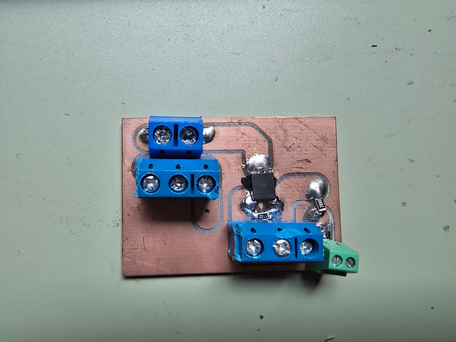
The heater is switched by an Infineon BSC009NE2LS5ATMA1, an N-channel OptiMOS power MOSFET in a PG-TDSON-8 package (the footprint visible in the PCB below). I chose this specific part for a few concrete reasons:
- Extremely low on-resistance (RDS(on) ≈ 0.9 mΩ): at the ~8.3 A the heater draws, the power dissipated in the MOSFET (I²·R) is only a fraction of a watt, so it barely heats up and doesn't need a large heatsink.
- Logic-level gate: it turns fully on at low gate voltages, which is important because the gate is driven from a 3.3 V class logic signal through the driver network.
- High current / voltage margin: its rated drain current and 25 V VDS rating give plenty of headroom over the 12 V / 8.3 A load, so the device runs well within safe limits.
- N-channel, low-side switching: placing the MOSFET between the heater's negative terminal and ground (low-side) lets a logic-level N-channel device switch the load efficiently.
Why the Other Components
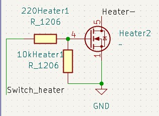
The driver stage around the MOSFET uses two resistors, both in 1206 packages, each with a clear job:
- 220 Ω gate resistor (220Heater1): in series with the gate, it limits the inrush current spike into the gate capacitance when switching, which protects the GPIO pin and slows the edge slightly to reduce ringing and noise.
- 10 kΩ pull-down resistor (10kHeater1): from gate to ground, it guarantees the gate is pulled LOW whenever the ESP32 pin is floating (for example during boot or reset), so the heater can never switch on accidentally. This is a critical safety component for a heater.
Why These Resistor Values
The two values were not arbitrary — each is a balance between two competing effects:
- Why 220 Ω for the gate, and not less or more: the gate behaves like a small capacitor, and at the instant of switching the GPIO pin briefly sees almost a short circuit into that capacitance. With a 3.3 V drive, a 220 Ω resistor limits that peak gate current to roughly 3.3 V ÷ 220 Ω ≈ 15 mA, which is safely within the ESP32 pin's limit. A smaller resistor (e.g. 22 Ω) would let a much bigger current spike stress the pin and create ringing; a much larger resistor (e.g. 1 kΩ) would slow the switching edge so much that the MOSFET spends longer in its partially-on, high-dissipation region. 220 Ω sits in the sweet spot: it protects the pin and tames ringing while still switching fast enough that the MOSFET barely heats up.
- Why 10 kΩ for the pull-down: its only job is to drain the gate to 0 V when the ESP32 pin is not actively driving it, so it must be large enough that it doesn't "fight" the GPIO or waste current when the pin drives the gate HIGH, but small enough to reliably hold the gate low against tiny leakage currents. 10 kΩ is the standard compromise: when the pin drives 3.3 V it only wastes 3.3 V ÷ 10 kΩ ≈ 0.33 mA (negligible), yet it's a low enough resistance to keep the gate firmly at 0 V during boot, reset or any time the pin is floating — keeping the heater safely off.
PCB Layout
KiCad
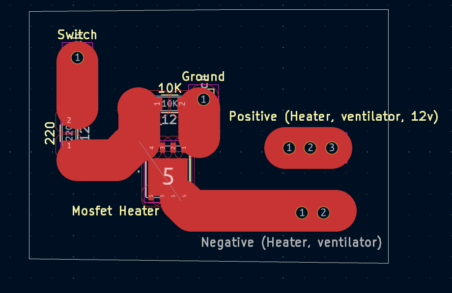
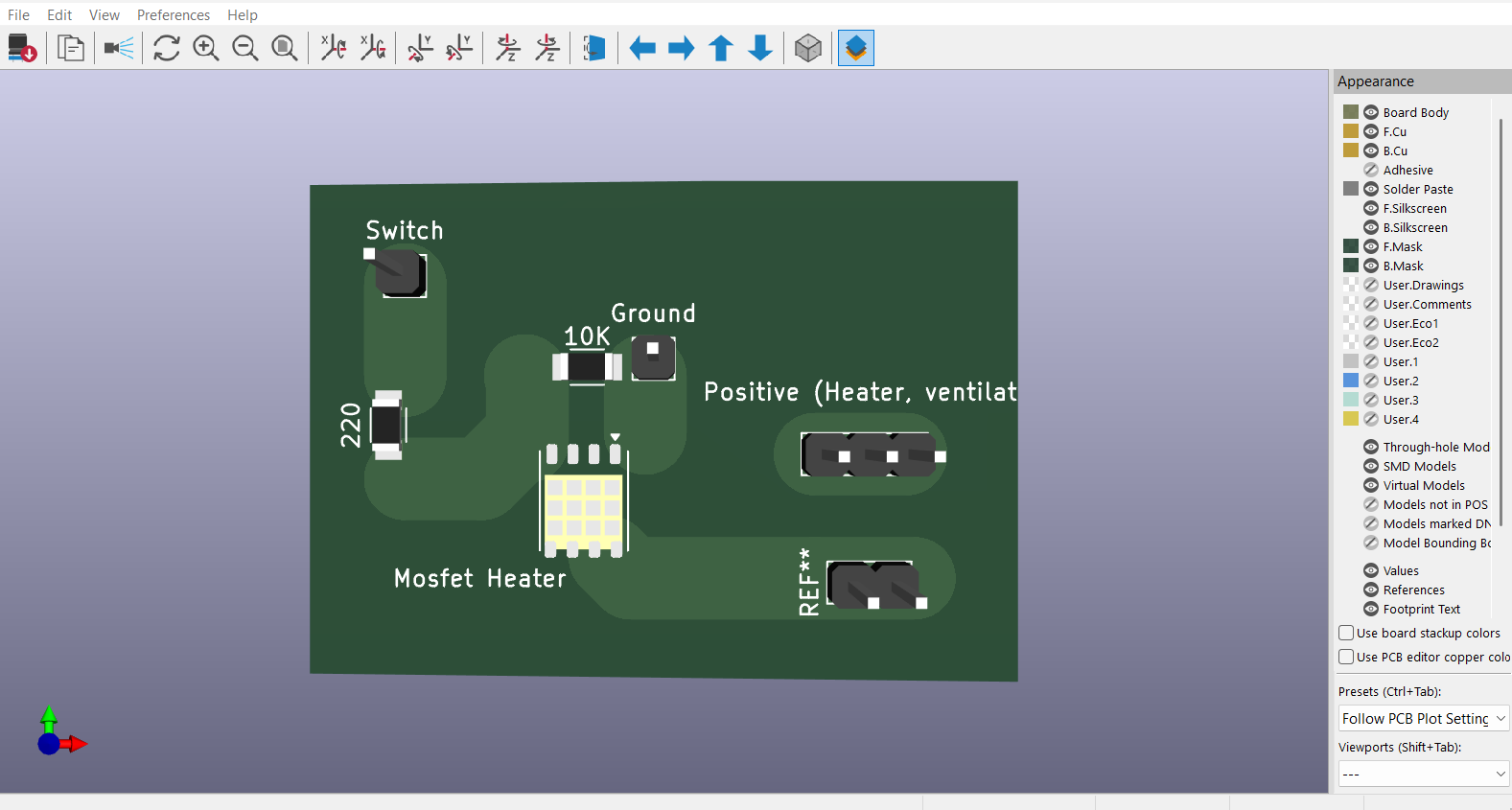
The driver was laid out as a small dedicated board. The MOSFET sits in the center (PG-TDSON-8 footprint), with the 220 Ω and 10 kΩ resistors next to the gate, the switch input on one side, and the high-current connectors — Positive (Heater, ventilator, 12 V) and Negative (Heater, ventilator) — on the edges.
3D View
Track Width — KiCad Calculator
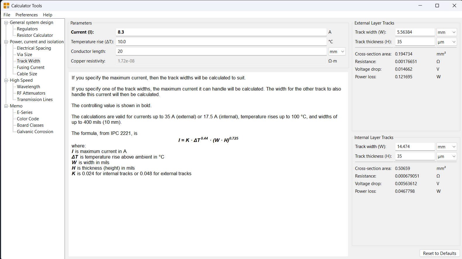
Because the heater path carries roughly 8.3 A, the traces on that path cannot be the default thin signal width. I used the KiCad PCB Calculator (Track Width tab), which implements the IPC-2221 standard with the formula I = K · ΔT0.44 · (W · H)0.725. I entered my real parameters:
- Current (I): 8.3 A
- Temperature rise (ΔT): 10 °C
- Conductor length: 20 mm
- Track thickness (H): 35 µm (standard 1 oz copper)
For an external-layer track the calculator returned a required track width of about 5.56 mm, with a very low resistance (~0.0018 Ω), voltage drop (~0.015 V) and power loss (~0.12 W) — confirming the wide trace stays cool. Based on this result I made the heater/power traces clearly wider than the signal traces, which is why the high-current paths look noticeably thicker in the layout, while the gate and control signals stayed at the normal narrow width.
Connections
Hardware
The heater is switched on the low side with a logic-level N-channel MOSFET. The ESP32 drives the MOSFET gate, while the temperature is read from an SHT31 sensor over I²C.
| Signal | Connection |
|---|---|
| MOSFET gate | GPIO 0 (through a gate resistor) |
| MOSFET drain | Heater negative terminal |
| MOSFET source | GND (common with 12 V supply and ESP32) |
| Heater positive | 12 V supply |
| SHT31 SDA / SCL | GPIO 4 / GPIO 5 (I²C @ 0x44) |
GPIO 0 was used as the gate control pin. A common ground between the 12 V supply, the heater, the MOSFET source and the ESP32 is essential for the gate voltage to be referenced correctly.
Components & Sourcing
Fabrication Data
The table below lists the components used on the driver board, their function, and where I sourced each one for fabrication.
| Component | Function | Source / Where I got it |
|---|---|---|
| MOSFET — BSC009NE2LS5ATMA1 (PG-TDSON-8) | N-channel low-side switch for the heater | University lab |
| Resistor 220 Ω (1206) | Gate series resistor | University lab |
| Resistor 10 kΩ (1206) | Gate pull-down (safe-off) | University lab |
| PTC heater 100 W / 12 V | Heating output device | Amazon MX |
| SHT31 sensor | Temperature feedback (I²C) | Amazon MX |
| Copper-clad board / connectors | PCB substrate and wiring | University lab and Steren |
Code
Arduino IDE
The following code reads the temperature from the SHT31 and switches the heater with hysteresis control:
#include <Arduino.h>
#include <Wire.h>
#include <Adafruit_SHT31.h>

Adafruit_SHT31 sht31 = Adafruit_SHT31();

const int Pin_Heater = 0;

const float Setpoint = 45.0;   // target temperature in C
const float Hysteresis = 2.0;  // half-band in C

bool heaterState = false;

void setup() {
  pinMode(Pin_Heater, OUTPUT);
  digitalWrite(Pin_Heater, LOW);  // safe boot: heater off

  Serial.begin(115200);
  Wire.begin(4, 5);              // SDA, SCL

  sht31.begin(0x44);
}

void loop() {
  float t = sht31.readTemperature();

  if (isnan(t)) {
    digitalWrite(Pin_Heater, LOW);  // sensor fault: heater off
    heaterState = false;
    delay(1000);
    return;
  }

  if (t < Setpoint - Hysteresis) {
    heaterState = true;
  } else if (t > Setpoint + Hysteresis) {
    heaterState = false;
  }
  // inside the band: keep previous state

  digitalWrite(Pin_Heater, heaterState ? HIGH : LOW);

  Serial.print("T: ");
  Serial.print(t);
  Serial.print(" C  Heater: ");
  Serial.println(heaterState ? "ON" : "OFF");

  delay(1000);
}
Code Explanation
Analysis
Library Import
The code includes the required libraries:
Arduino.hfor standard Arduino functions.Wire.hfor the I²C bus used by the sensor.Adafruit_SHT31.hto read the temperature/humidity sensor.
Pin and Control Constants
The MOSFET gate is connected to GPIO 0, and two constants define the control behavior:
const int Pin_Heater = 0;
const float Setpoint = 45.0;
const float Hysteresis = 2.0;
The setpoint is the target temperature. The hysteresis is the half-width of the dead band around it, so the heater effectively switches between 43 °C and 47 °C.
Setup Function
In setup() the gate pin is driven LOW before anything else, so a reset or
brown-out can never leave the heater energized by accident. Then the serial port and the I²C bus
are initialized, and the sensor is started at address 0x44.
Sensor Fault Handling
The SHT31 occasionally returns NaN. If the reading is invalid, the heater is forced off: running a heater blind is the most dangerous state of the system, so a bad reading must never keep it on.
if (isnan(t)) {
  digitalWrite(Pin_Heater, LOW);
  ...
}
Hysteresis Control
The control logic turns the heater on below setpoint − hysteresis and off above setpoint + hysteresis. Inside the band it keeps its previous state:
if (t < Setpoint - Hysteresis) {
  heaterState = true;
} else if (t > Setpoint + Hysteresis) {
  heaterState = false;
}
This avoids the rapid on/off chatter that a single threshold would cause, protecting both the MOSFET and the heater. A PID loop was considered, but a thermal chamber is a slow, heavily damped system, so hysteresis reaches the same steady state with a single tunable parameter.
Result
Thermal Test
The final result was a heater that maintained the chamber temperature around the 30 °C setpoint within the ±2 °C band, switching cleanly without rapid chatter.
Monitoring the serial output confirmed the loop behaved as expected: the heater turned on when the temperature dropped below the band and off when it rose above it.
- Stable temperature held within the hysteresis band
- Clean switching with no relay/MOSFET chatter
- Heater forced off on sensor fault
Reflection
This week helped me understand how a microcontroller can drive a high-power output that no GPIO pin could switch directly, and how an output device that affects the environment requires sensor feedback to be controlled safely.
Working with a heater also forced me to think about safety from the start: safe boot states, sensor fault handling, and the self-limiting nature of the PTC element. These ideas carry directly into the multi-layer safety design of my final project.
This assignment reinforced the relationship between software and hardware: the control logic, the MOSFET driver stage and the sensor feedback all had to work together for the heating subsystem to behave predictably.