As part of this week, our group worked together on the electronics production group assignment — characterizing the lab's PCB milling process by running test cuts to measure trace widths, clearances, and the machine's design rules, then documenting our shared findings before fabricating our individual boards. You can read the complete group assignment, including the test results and our shared documentation, here:
Group AssignmentGroup Assignment
Project Overview
PCB Milling
For this week I fabricated the same PCB designed during Week 6. The goal was to move from the electronic schematic and PCB layout into a real, manufacturable board. Instead of sending the design to an external PCB manufacturer, I used in-house digital fabrication to mill the traces directly on a copper board.
The workflow combined several tools: the board design from Week 6, SVG preparation in Inkscape, toolpath generation with mods, and physical machining in the Roland SRM-20. Mods provides a prepared workflow for Roland SRM-20 PCB milling and can take SVG input to generate the machine file.
This week was important because it connected design decisions from the previous week with the physical limitations of PCB production: trace width, isolation, cut depth, and the real precision of the machine.
Board Used
Week 6 PCB
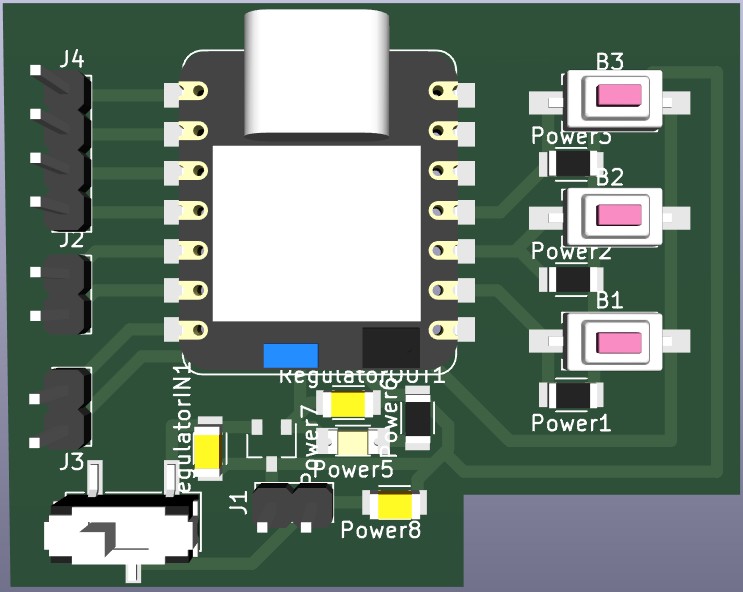
The board milled in this assignment is the same custom PCB developed in Week 6. That means the fabrication process was not isolated from design: it was a continuation of the previous workflow. By manufacturing the same board, I could validate whether the electronic design decisions were compatible with subtractive PCB production.
This is especially valuable because PCB milling imposes practical constraints. A board may look correct in the CAD environment, but during fabrication issues such as traces that are too close, pads that are too small, or footprints that are difficult to solder may appear. Milling the Week 6 PCB allowed me to verify the board as a real physical object.
File Preparation
KiCad → PDF → Inkscape → SVG
How I Got the SVG
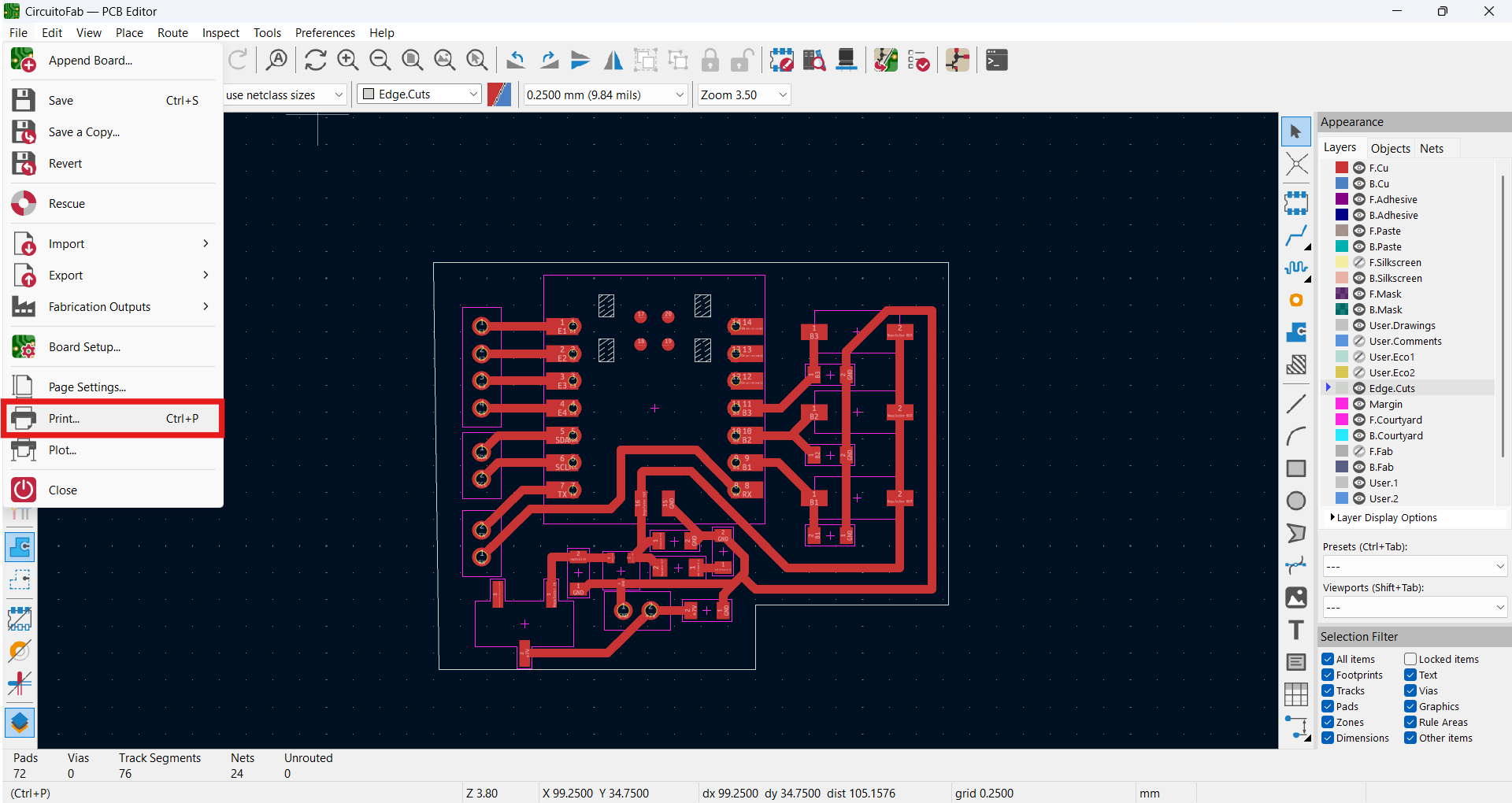
The milling workflow in mods needs a clean vector or image of the board, so the first task was to turn my KiCad board into an SVG. I did this in a chain of three steps: KiCad → PDF → Inkscape → SVG.
1. Print the copper layer from KiCad as PDF
In the KiCad PCB Editor I opened File → Print (Ctrl+P).
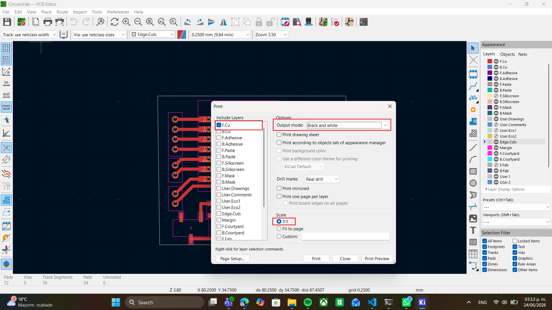
Inside the Print dialog I configured three critical options so the output would be usable for milling:
- Include Layers → F.Cu only: I selected just the front copper layer, since that is the layer whose traces will be milled. All other layers were left unchecked.
- Output mode → Black and white: this gives a clean two-tone image (copper vs. background) that converts cleanly into a milling path, with no colors to confuse the toolpath.
- Scale → 1:1: this is essential. The board must be printed at real size so the final milled PCB matches the exact dimensions of the design and the component footprints.
With these set, I printed to PDF.
2. Open the PDF in Inkscape and export as SVG
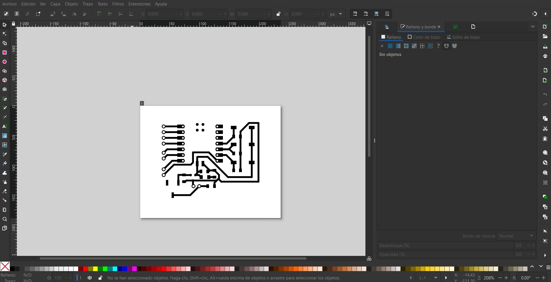
I then opened that PDF in Inkscape. Because a PDF is already vector-based, Inkscape imports the traces as real vector geometry. There I made sure the artwork was clean — the traces clearly defined, the board outline separated from the trace geometry, the scale preserved, and any unnecessary elements removed — and then saved/exported the file as an SVG. This SVG is the file that mods reads to generate the toolpath.
Toolpath Generation
modsproject.org
Configuring mods
With the SVG ready, I went to modsproject.org to generate the milling file for the Roland SRM-20. Mods is a browser-based fabrication environment that chains small "modules" together into a workflow — each module does one task and passes its result to the next. Below I explain each step and, in detail, every box the user actually has to modify.
1. Open the correct program
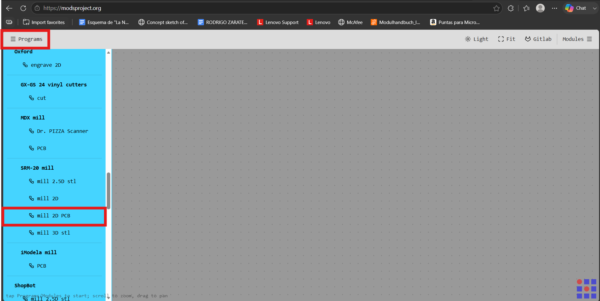
I clicked Programs (top-left) to open the program list. Then I scrolled down to the SRM-20 mill group and selected mill 2D PCB. This is the key choice: it loads the complete pre-built workflow specifically for milling PCBs on the SRM-20, with all the modules already connected.
2. Load the SVG
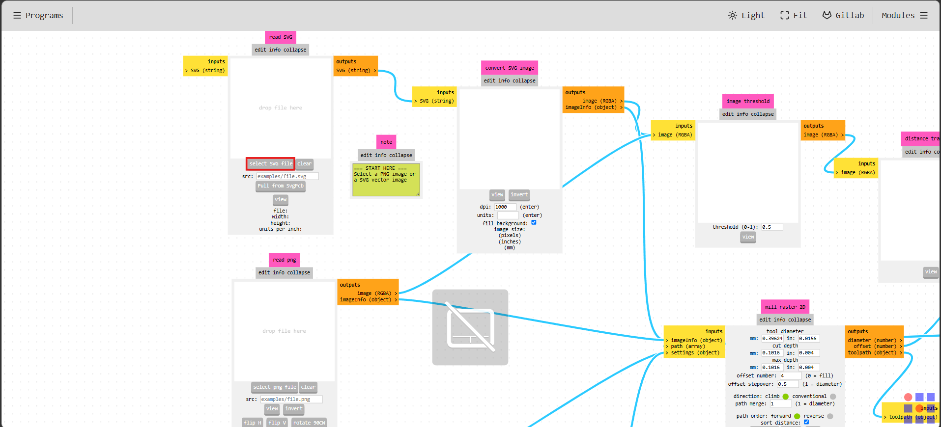
In the read SVG module I clicked select SVG file (highlighted) and loaded the SVG I exported from Inkscape. This is where the board geometry enters the workflow — mods reads the black/white image to know where copper must stay and where it must be removed. You can either drop the file in the box or use this button to browse for it.
3. The modules you actually edit
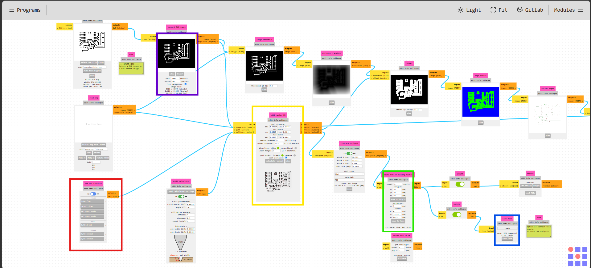
Once the workflow is loaded, these are the four boxes the user modifies — each highlighted in the image below:
- Set PCB defaults (red) — the tool selector: this is where you pick the operation and tool. Under traces you choose the engraving bit — 1/64" flat for the copper traces (or a V-bit for finer work); under drill you pick the drill size; and under cutout you choose 1/32" or 1/16" cutout to cut the board outline. Choosing a tool here automatically sets the correct tool diameter, number of offsets and cut depth for that operation, which is why you run the traces first with the fine bit and then switch to the cutout tool.
- Convert SVG image (purple) — resolution & size: this module rasterizes the SVG. The boxes you set are dpi (I used 1000, which controls the resolution/precision of the milling image), units, and the fill background checkbox. It also reports the resulting image size in pixels, inches and mm, so you can confirm the board came in at the correct real-world dimensions (1:1).
- Mill raster 2D (yellow) — the cutting parameters: this is the core toolpath module, and the values here decide how the copper is actually carved. The boxes you set are the tool diameter (filled in automatically from the tool you picked, e.g. 0.39624 mm for the 1/64" bit), the cut depth (how deep each pass goes, ~0.1016 mm for traces), the max depth (total depth to reach), the offset number (4 = how many passes of copper are cleared around each trace; 0 means "fill" / clear all copper), and the offset stepover (0.5 = how much the passes overlap, where 1 = one full tool diameter). You also choose the milling direction (climb vs. conventional) and the path order. Finally you press Calculate here to generate the toolpath preview shown at the bottom of the module.
- Roland SRM-20 milling machine (green) — speed & origin: this is the machine output module. Here you set the speed (mm/s) and, most importantly, the origin x / y / z values, which tell the job where the cut begins relative to the point you zeroed on the machine. It also has move to origin, a home position, move to home, and shows the estimated time for the job.
- Save file (blue) — export the .rml: after everything is configured you press Calculate on the mill raster 2D module to generate the toolpath, and then use this save file module to export the .rml file (it shows the file name and size). That .rml is what you load into the SRM-20.
The reason the traces and the outline are separated is that they use different tools and different depths: the traces are a shallow engraving with a fine bit, while the outline (cutout) is a deeper cut all the way through the board with a larger bit. So in practice you configure and save the traces first, mill them, then come back, switch the tool selector to the cutout tool, recalculate, save a second .rml, and mill the outline.
4. Toolpath preview — how the milled board will look
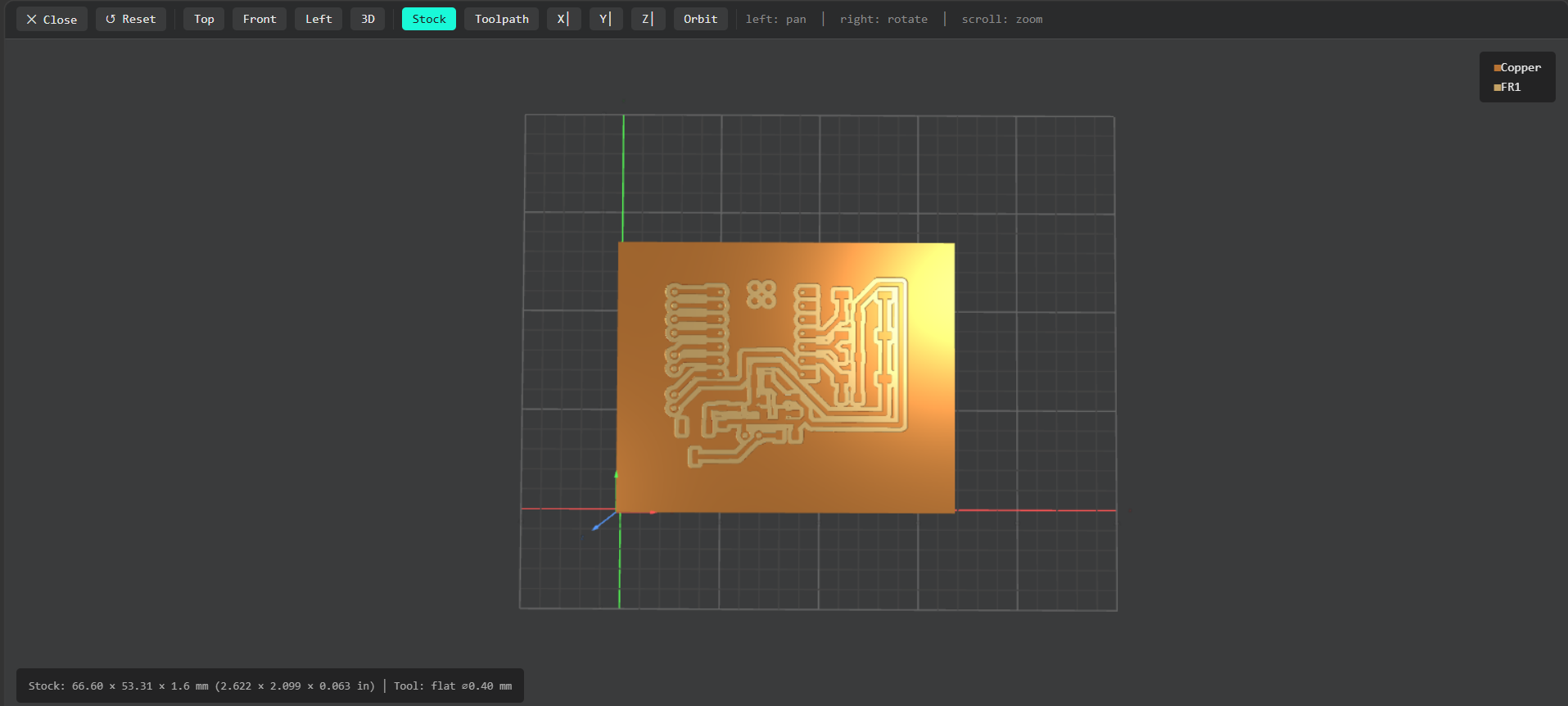
Before sending anything to the machine, mods shows a preview of the calculated toolpath at the bottom of the mill raster 2D module. This preview is very useful because it shows how the board will actually look once milled: where the tool will remove copper (the isolation around each trace) and where the copper will remain. Checking this preview lets me catch problems — traces that did not separate, areas that were not cleared, or an outline in the wrong place — before wasting a copper board and machine time.
Machine
Roland SRM-20
Calibrating the SRM-20 Mill
The PCB was fabricated using the Roland SRM-20, a 3-axis desktop milling machine widely used for PCB production in Fab Labs. The most important part of using it is the setup and calibration, because PCB milling removes only a very thin layer of copper and is extremely sensitive to the Z height. This is how I calibrated it, step by step:
Step 1 — Fix the copper board
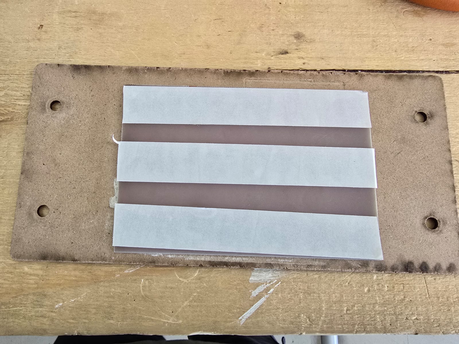
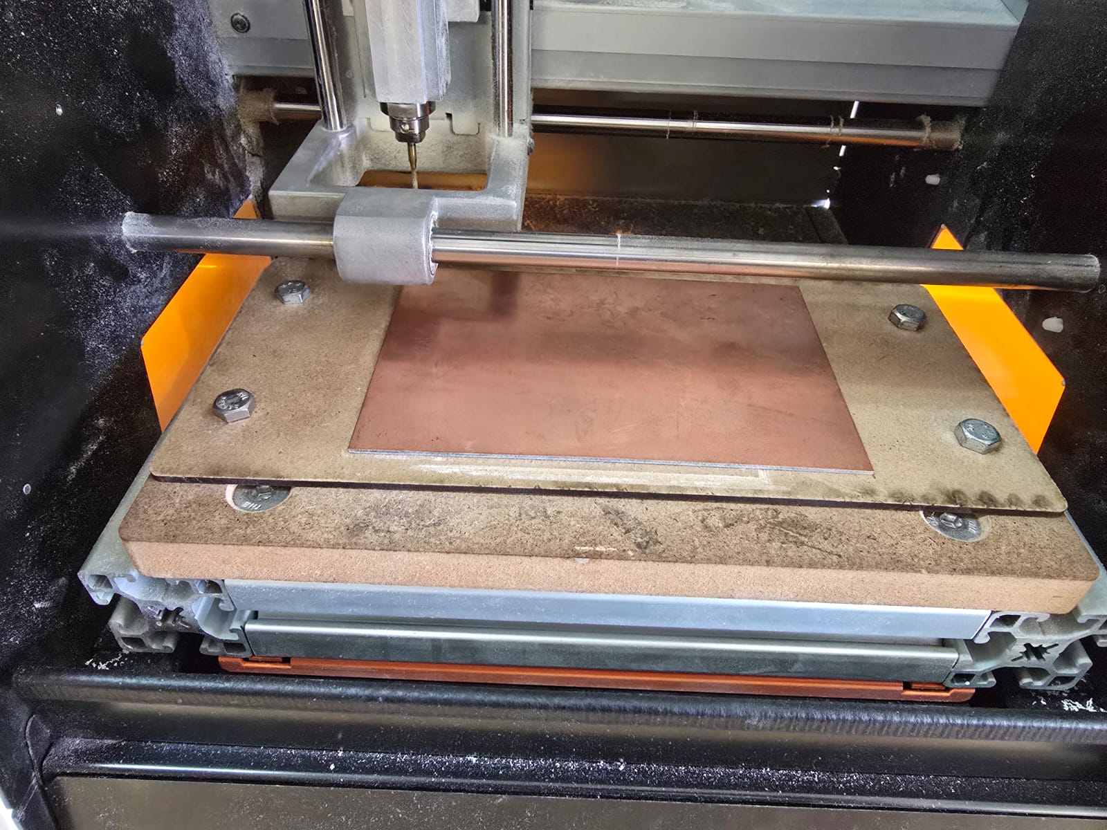
I secured the copper-clad board flat on top of a sacrificial layer on the bed using double-sided tape, making sure there were no bumps underneath, since any lift changes the cutting depth.
Step 2 — Install the tool
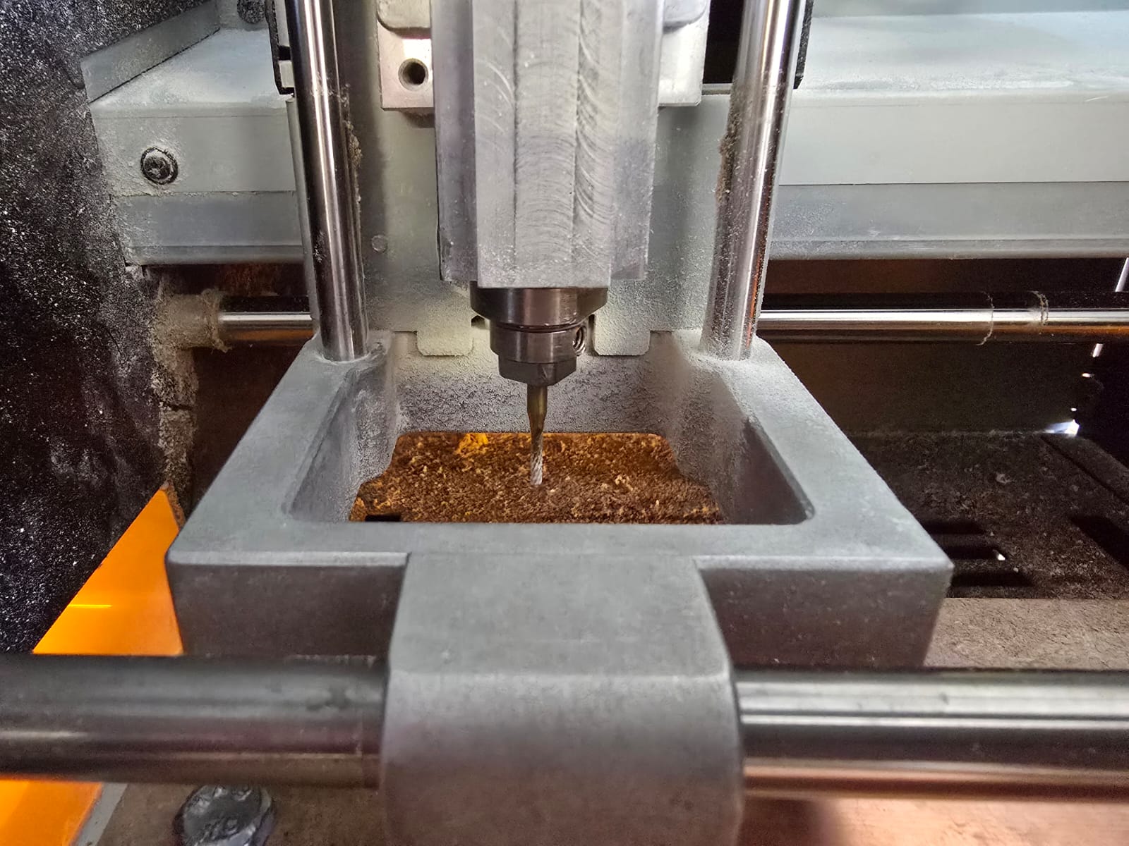
I mounted the 1/64" end mill for the traces, holding it in the collet but not fully tightening it yet, so I could still drop it onto the copper when setting the Z origin.
Step 3 — Set the X and Y origin
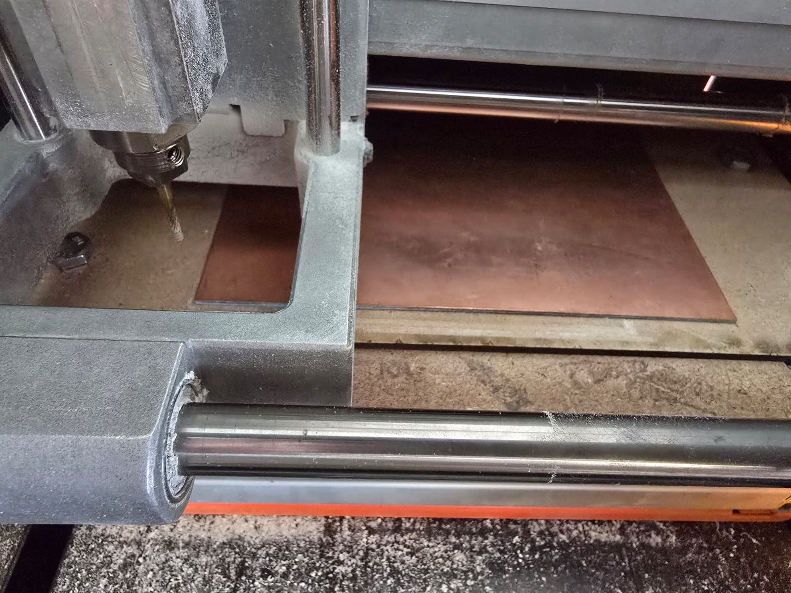
Using the SRM-20 control software (VPanel), I jogged the spindle to the corner of the board I chose as the origin and set X0 / Y0 there, matching the origin I had defined in mods.
Step 4 — Set the Z origin (most critical)
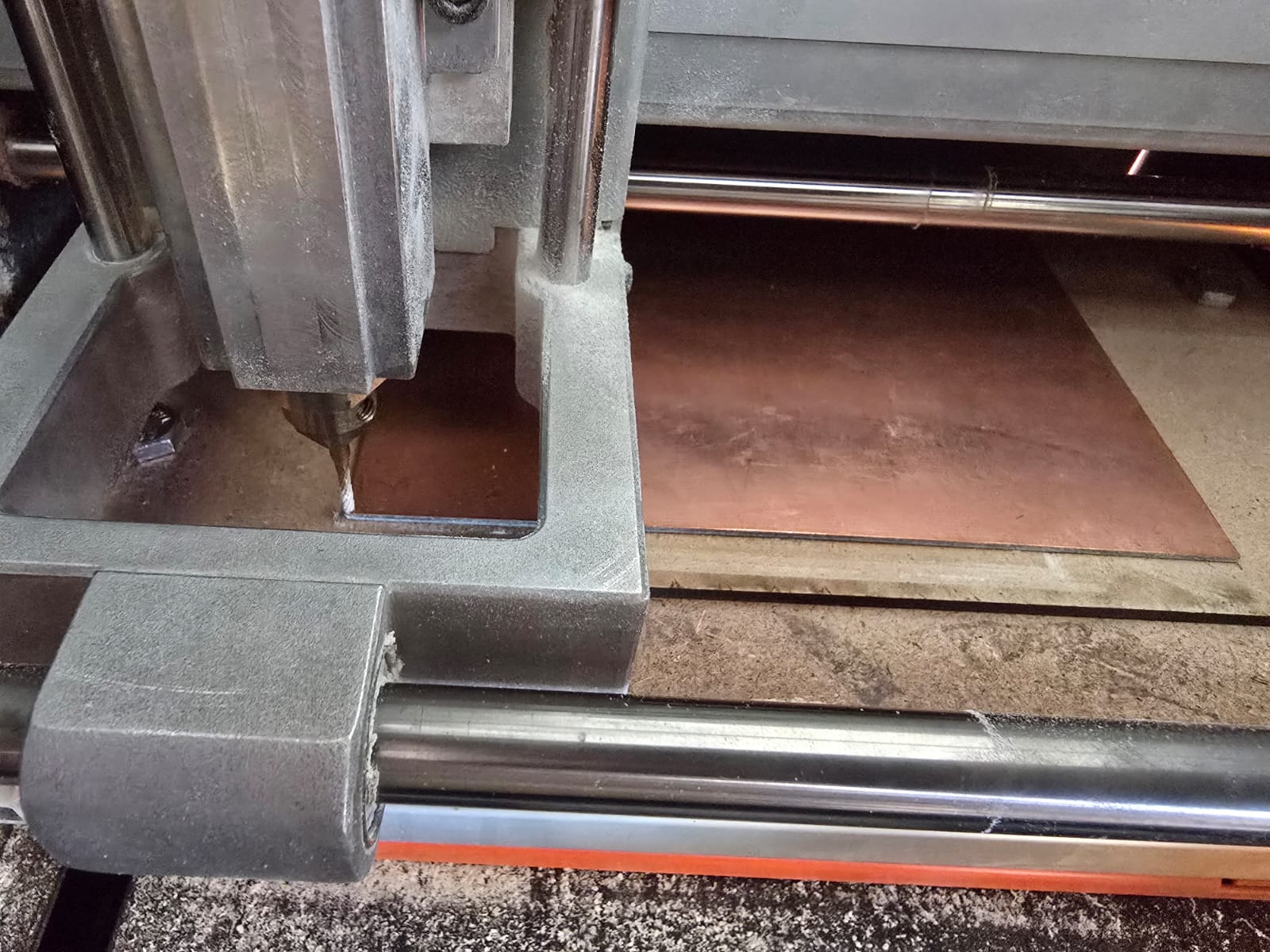
I jogged the spindle down close to the copper, then loosened the bit so it dropped and rested gently on the copper surface, and tightened it there. This sets Z0 exactly on the surface so the engraving depth is consistent across the whole board. This is the most important step: since PCB milling removes a very small amount of copper, even a small error in Z can leave traces that are not isolated (too shallow) or cuts that go too deep into the board.
Step 5 — Send the traces job first
I loaded the traces .rml file and started cutting. The fine 1/64" bit engraves the isolation around the traces.
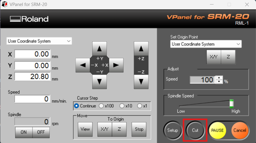
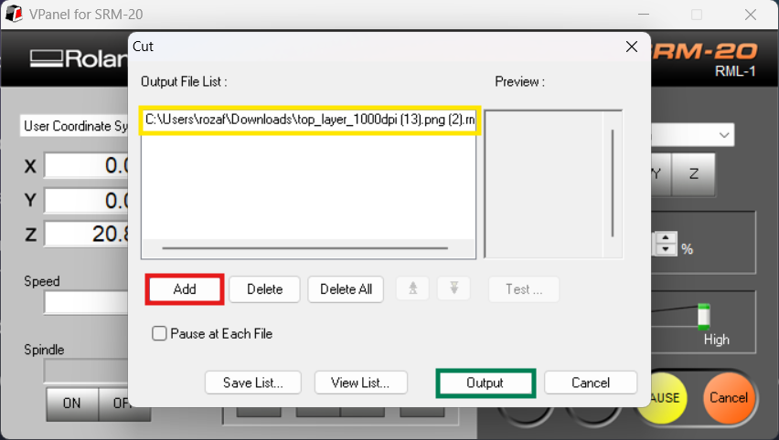
Red: Add, that means I added the trace I want to do.
Yellow: It is the trace that is uploaded.
Green: Output, when you click it it will start the milling process.
Fabrication Process
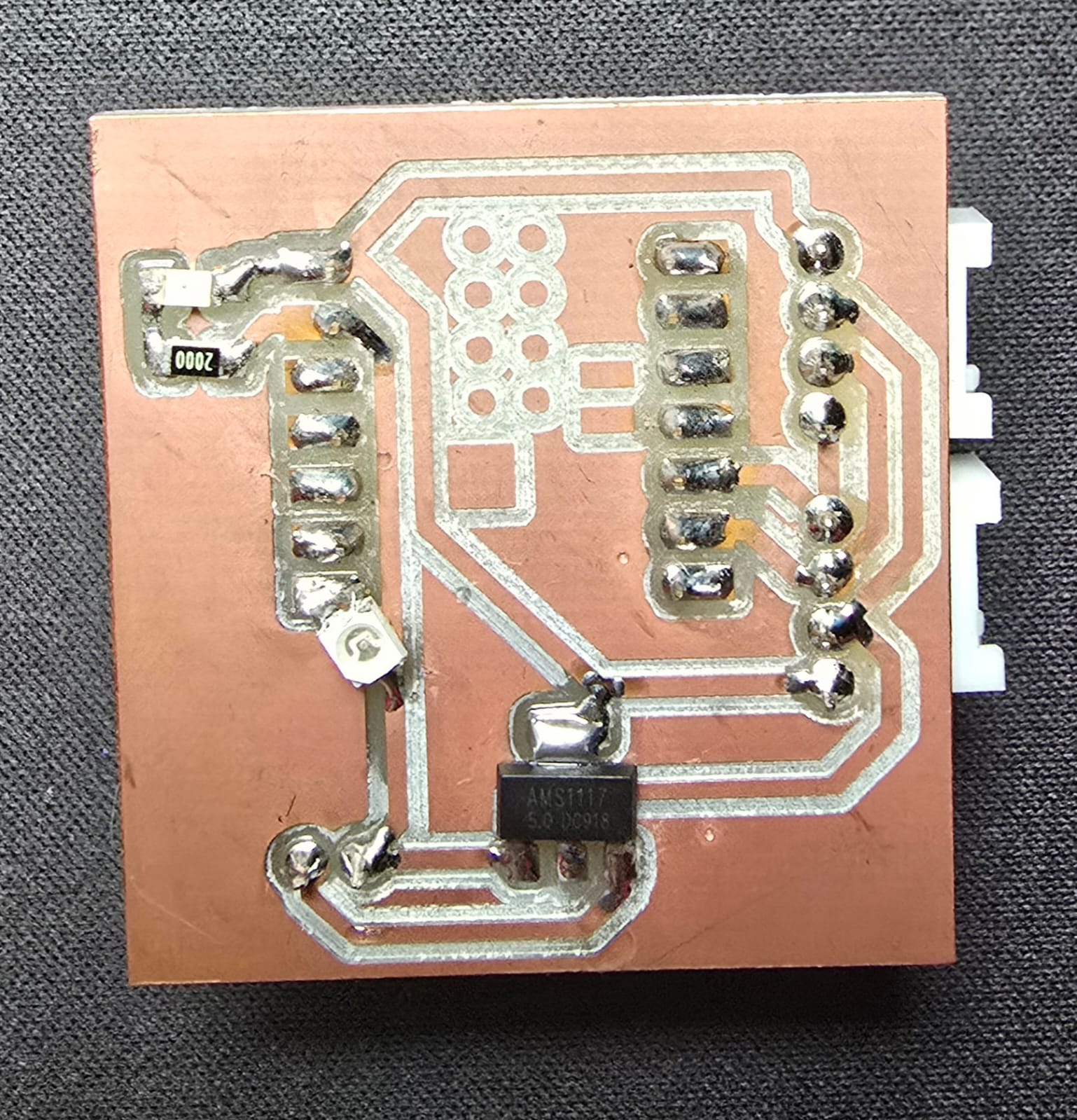
Finished PCB
Soldering
Assembly
Soldering the Components
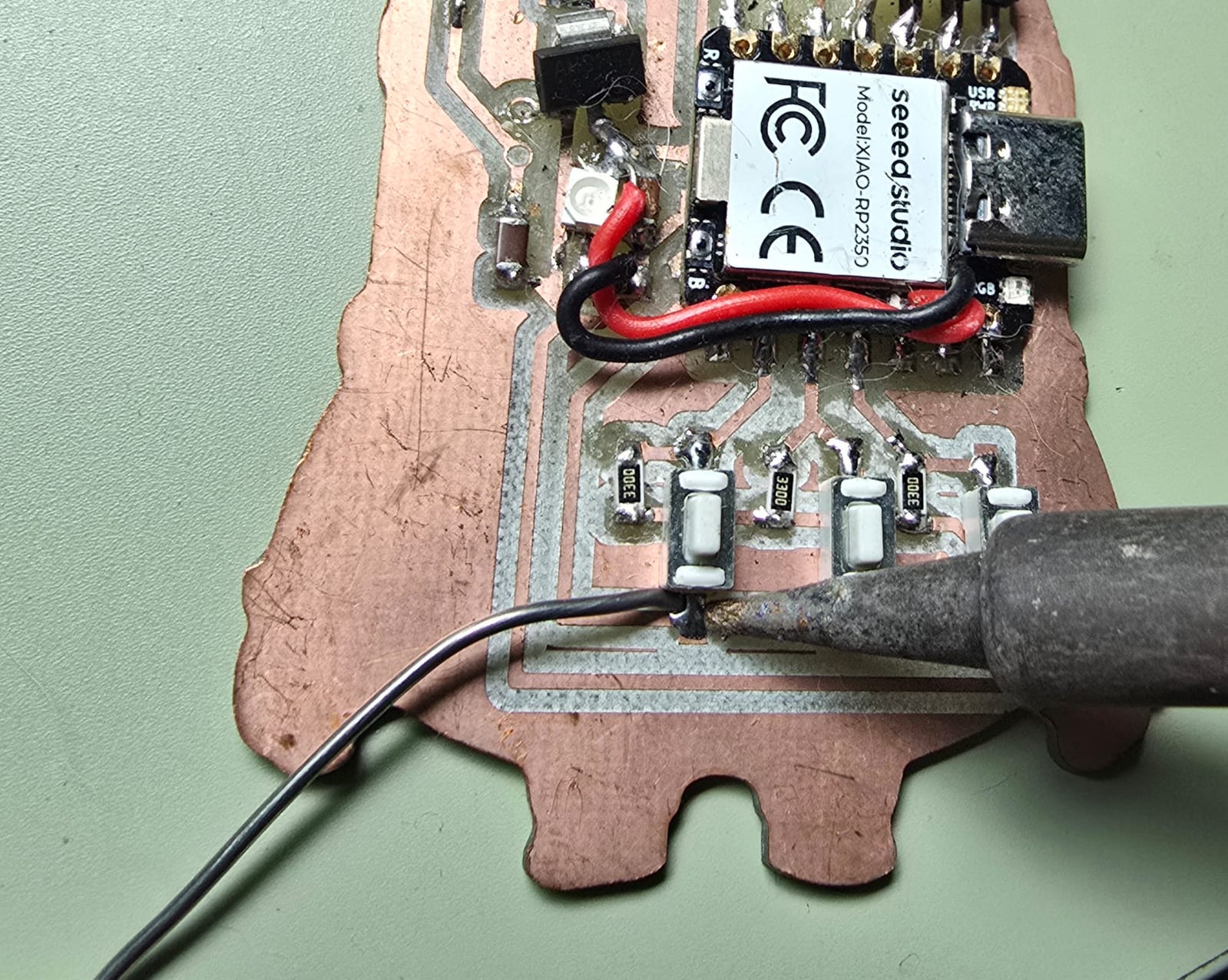
Once the board was milled and cut out, I soldered the components: the XIAO RP2350 microcontroller, the 330 Ω resistors, the LED and the wires. Soldering attaches each component electrically and mechanically to the copper pads.
Solder and iron settings I used
I used 63/37 solder with rosin core and set the soldering iron to 320 °C. The 63/37 alloy is a eutectic solder, which means it goes straight from solid to liquid (and back) at a single temperature without a pasty phase, so the joints solidify quickly and cleanly and there is less risk of a cold joint from the part moving while it cools. The rosin core provides flux right where it is needed, cleaning the copper and helping the solder flow. A tip temperature of 320 °C is hot enough to make good joints quickly on these small pads without staying so long that the pads or components overheat.
How to solder correctly
- Clean and tin the tip: a clean, lightly tinned soldering-iron tip transfers heat much better than a dirty oxidized one.
- Heat the pad and the pin together: place the tip so it touches both the copper pad and the component lead at the same time for a second or two. You heat the joint, not the solder.
- Feed the solder into the joint: touch the 63/37 rosin-core solder to the heated pad/pin (not directly to the tip) so it melts and flows around the joint by capillary action.
- Remove solder, then iron: pull the solder away first, then the iron, and let the joint cool without moving it. A good joint is shiny and forms a small concave "volcano" cone — not a round ball.
- Start with the hardest part: for SMD resistors I tinned one pad first, placed the component, re-heated that pad to tack it down, then soldered the opposite side.
A common mistake is a "cold joint" (dull, lumpy) which happens when there isn't enough heat or the joint moves while cooling; those need to be reheated. Too much solder bridging two pads must be removed with solder wick.
Programming
Blink Test
Loading the First Program (Blink)
To confirm the board worked, I loaded a simple Blink program — the classic first test that turns an LED on and off. If the LED blinks, it proves several things at once: the microcontroller is powered correctly, it accepts code over USB, and the LED and its 330 Ω resistor are soldered and routed correctly.
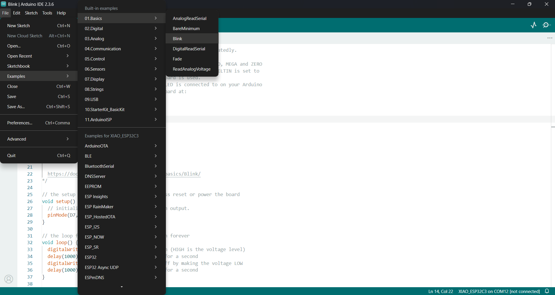
I did not write this program from scratch: Blink is one of the example sketches that comes built into the Arduino IDE. I opened it from File → Examples → 01.Basics → Blink, which loads the ready-made example directly into the editor.
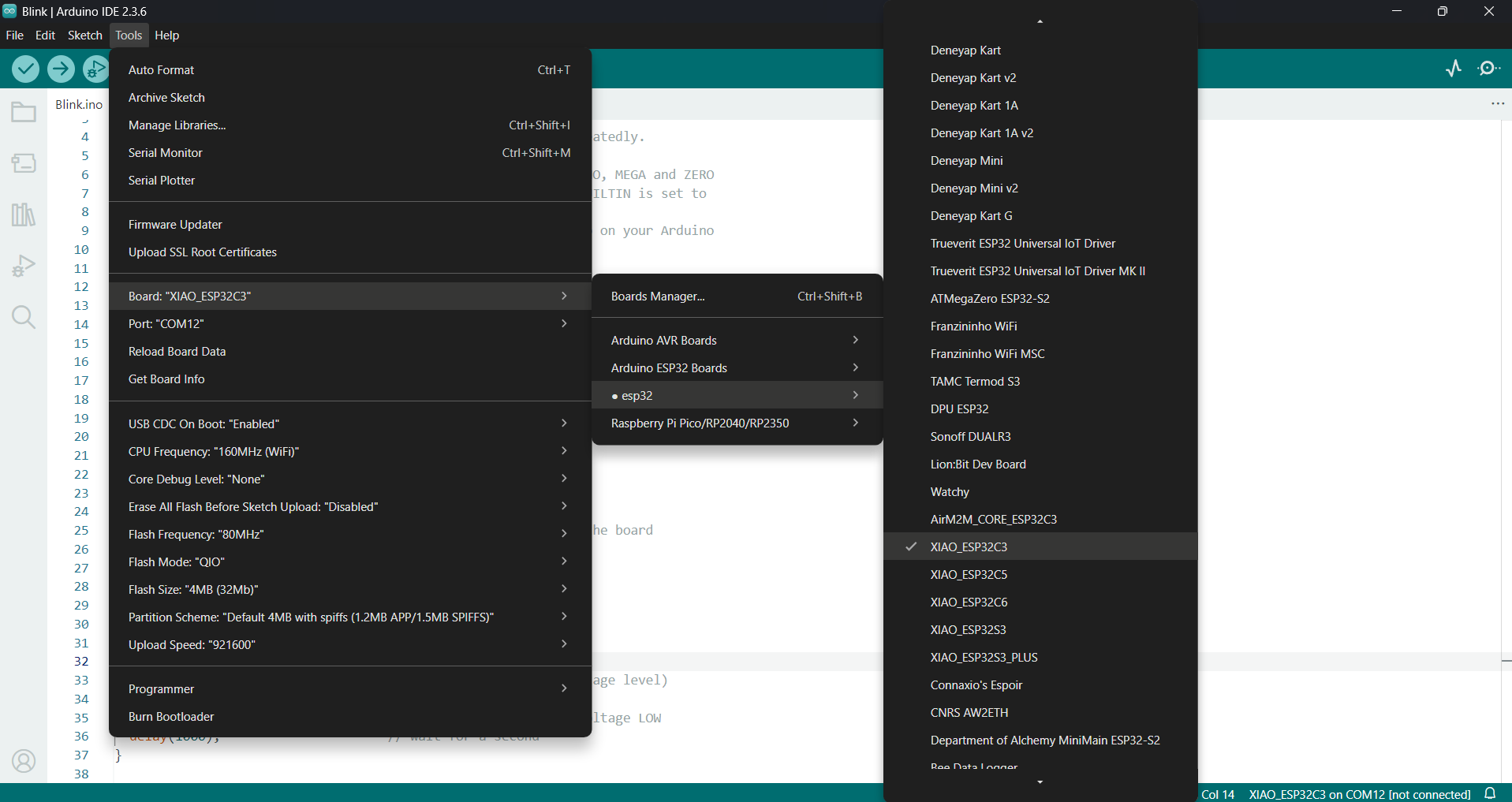
Before uploading, I had to select the correct board and port so the IDE knew what it was programming. I went to Tools → Board and selected the XIAO (XIAO RP2350), and then chose the matching Port that appeared when I connected the board over USB. Selecting the right board is essential, because it tells the IDE which microcontroller core and pin definitions to use when compiling.
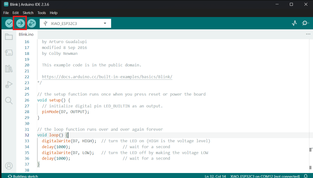
With the example open and the board selected, I pressed Upload. The board enumerated correctly and the LED started blinking on the first try.
Code
        void setup() {
          pinMode(D7, OUTPUT);
        }

        void loop() {
          digitalWrite(D7, HIGH);
          delay(1000);
          digitalWrite(D7, LOW);
          delay(1000);
        }
Result — LED Blinking
The blink test confirms the milled board is fully functional: power, programming and the LED circuit all work.
Problem & Second Board
Design Iteration
The first board was not done the right way
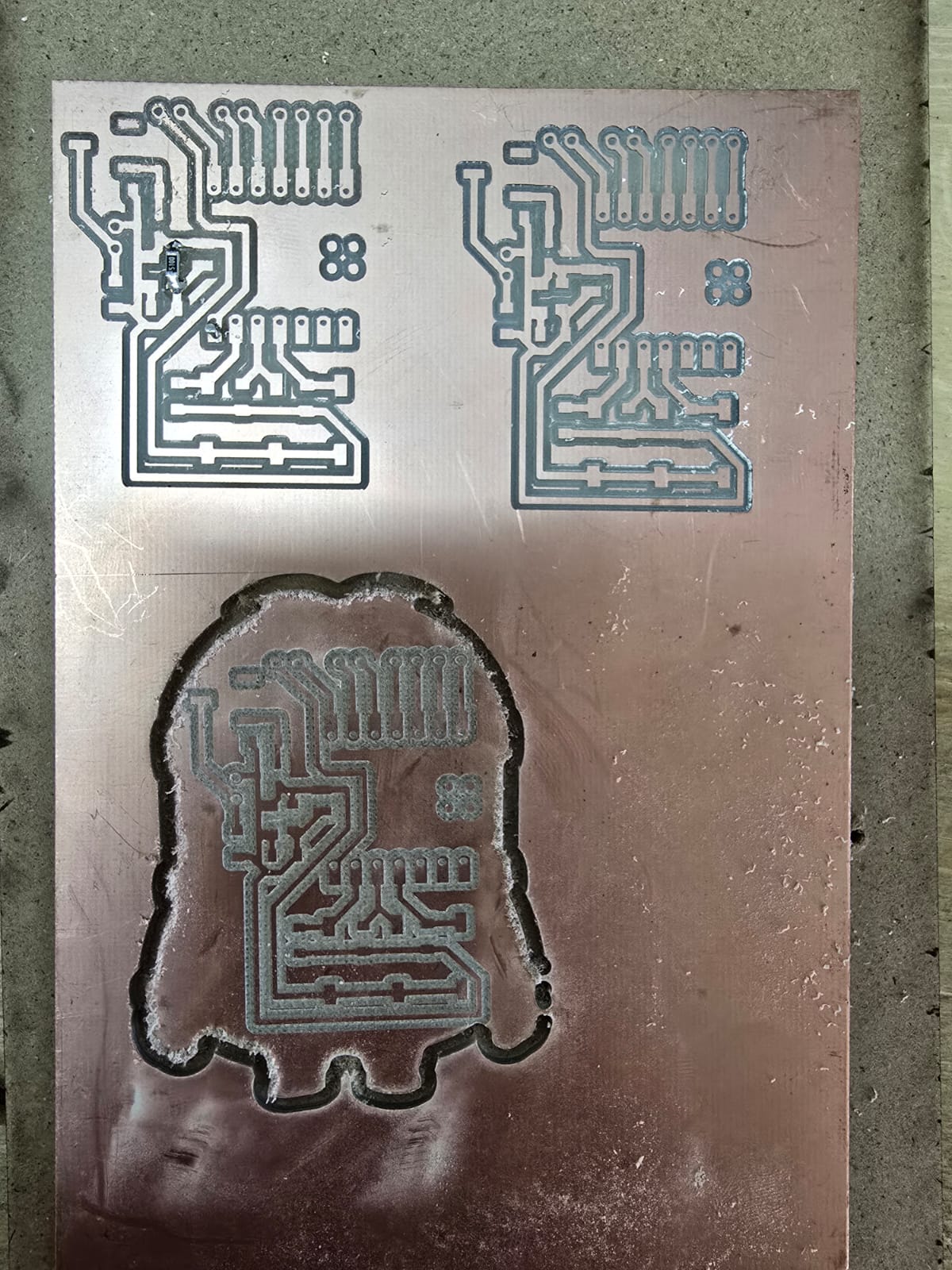
The board shown in all the images above is my first design. It was not done the correct way: when I laid out the board, I routed the power to the bottom row of pins of the XIAO, and those bottom pins could not deliver power to the board properly. Because the power path was not routed correctly, the board did not get powered the way it should through the traces alone.
As a temporary workaround I had to bridge the power with jumper wires, routing it by cable to where it actually needed to go. That made it work for the test, but relying on jumper wires instead of the routed copper is not the correct way to do it — so I decided to redo the board properly.
The second board — a new, correct design
So I made a completely new second design, this time routing the power the correct way so it no longer depended on the problematic bottom pins of the XIAO, and I tidied the whole layout. To fabricate it I followed exactly the same steps as at the beginning: I designed the new board in KiCad, printed the F.Cu layer to PDF (black and white, 1:1), opened it in Inkscape and exported the SVG, generated the toolpath in mods, and milled it on the Roland SRM-20 with the same calibration process. The only thing that changed was the design — the workflow was identical.
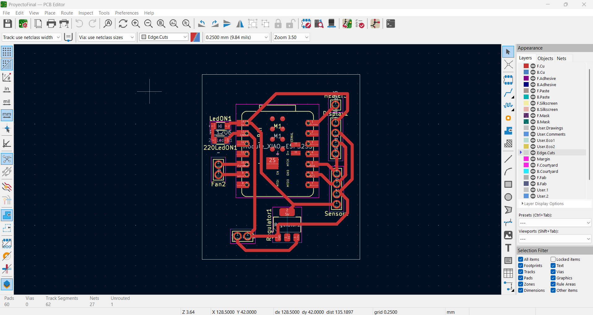
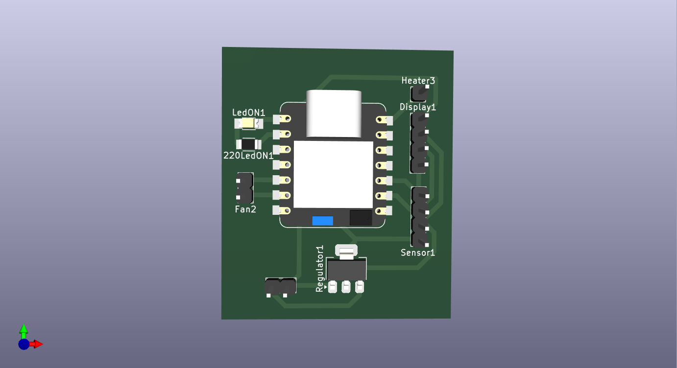
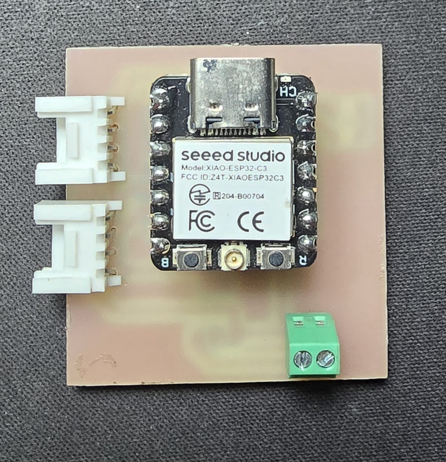
Following the same fabrication steps on a correctly routed design gave the result I wanted: with the power routed the right way, the second board powered up directly from its own traces, with no jumper wires needed. This is the version I consider the finished, clean result of the week.
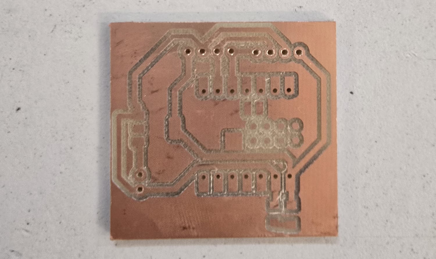
The most useful lesson here was that a board can look right in CAD and still be done the wrong way in a subtle detail — in this case, which pins actually carry the power — and that the right fix is to go back to the design and re-run the same reliable process, rather than patching the hardware with cables.
Fabrication Process
Workflow
The complete fabrication process can be summarized as:
| Stage | Tool | Purpose |
|---|---|---|
| Board design | Week 6 PCB | Create the electronic layout |
| Vector preparation | KiCad (PDF) → Inkscape (SVG) | Generate and verify SVG geometry |
| Toolpath generation | Mods | Create machine-ready milling paths |
| Machining | Roland SRM-20 | Mill traces and cut board outline |
| Soldering | 63/37 rosin-core solder, iron at 320 °C | Attach components to the PCB |
| Programming | Arduino IDE (Blink example) | Verify the board is functional |
What I found most valuable in this workflow was the direct relationship between digital geometry and fabrication result. Any design decision became immediately visible in the milled board, which makes electronics production a very instructive fabrication process.
The code that I used on this PCB is the same as the previous one, the blink code, which is a simple program that turns an LED on and off at a regular interval. The fact that the same code worked confirmed that the design and fabrication were successful.
Reflection
This week helped me understand that PCB fabrication is not only about electronics, but also about manufacturing precision. Designing a board is one step; producing it successfully requires adapting the design to the milling process, the tool diameter, the machine calibration, and the material.
By fabricating the same PCB from Week 6, I was able to validate the continuity between electronic design and physical production. The combination of Inkscape, mods, and the SRM-20 made it possible to convert a digital board into a real object ready for the next stages of assembly and testing. The jump from the first board (which was not done the right way and had to be bridged with jumper wires) to a new, correctly routed second design also taught me that the right way to solve a routing mistake is back in the design — re-running the same reliable steps — not patching the hardware with cables.