As part of this week, our group worked together on the electronics design group assignment, comparing different EDA tools and workflows and documenting our shared findings before developing our individual boards. You can read the complete group assignment, including our comparisons and shared documentation, here:
Group AssignmentGroup Assignment
Electronic Architecture
XIAO RP2040
This week focused on designing a custom electronic board to support my final project. The design integrates a microcontroller, regulated power supply, input buttons, and communication headers.
The objective was to create a modular and expandable PCB that can be reused for control, sensing, and future expansion.
KiCad Workflow
Electronic CAD
The entire electronic design was developed using KiCad. This open-source Electronic Design Automation (EDA) software allows schematic capture, PCB layout design, component management, and fabrication file generation.
1. Project Creation
The first step was creating a new project inside KiCad. This automatically generates:
- .kicad_pro → Project file
- .kicad_sch → Schematic file
- .kicad_pcb → PCB layout file
This structure ensures that schematic and PCB remain synchronized.
2. Schematic Editor
Tool Used: Schematic Editor (Eeschema)
In the schematic editor, I created the logical representation of the circuit.
Key Tools Used:
- Add Symbol: Inserted XIAO RP2040, regulator, resistors, capacitors, buttons.
- Wire Tool: Connected electrical nets.
- Power Symbols: Added GND, +7V, Regulator OUT.
- Net Labels: Named connections to keep schematic clean.
- Annotate Tool: Automatically numbered components (R1, C1, U1).
- Electrical Rules Check (ERC): Verified missing or incorrect connections.
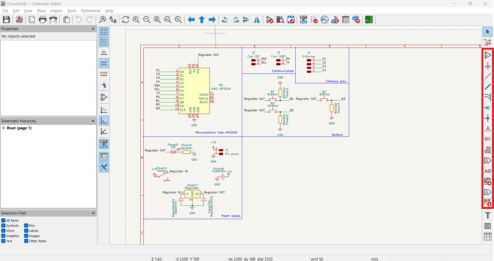
ERC was critical to detect floating pins and power issues before moving to PCB layout.
3. Assigning Footprints
Tool Used: Assign Footprints
After finishing the schematic, each symbol was assigned a physical footprint.
For example:
- Resistors → 1206 SMD footprint
- Capacitors → 1206 SMD footprint
- Voltage regulator → SOT-223 or equivalent
- XIAO RP2040 → Header-based footprint
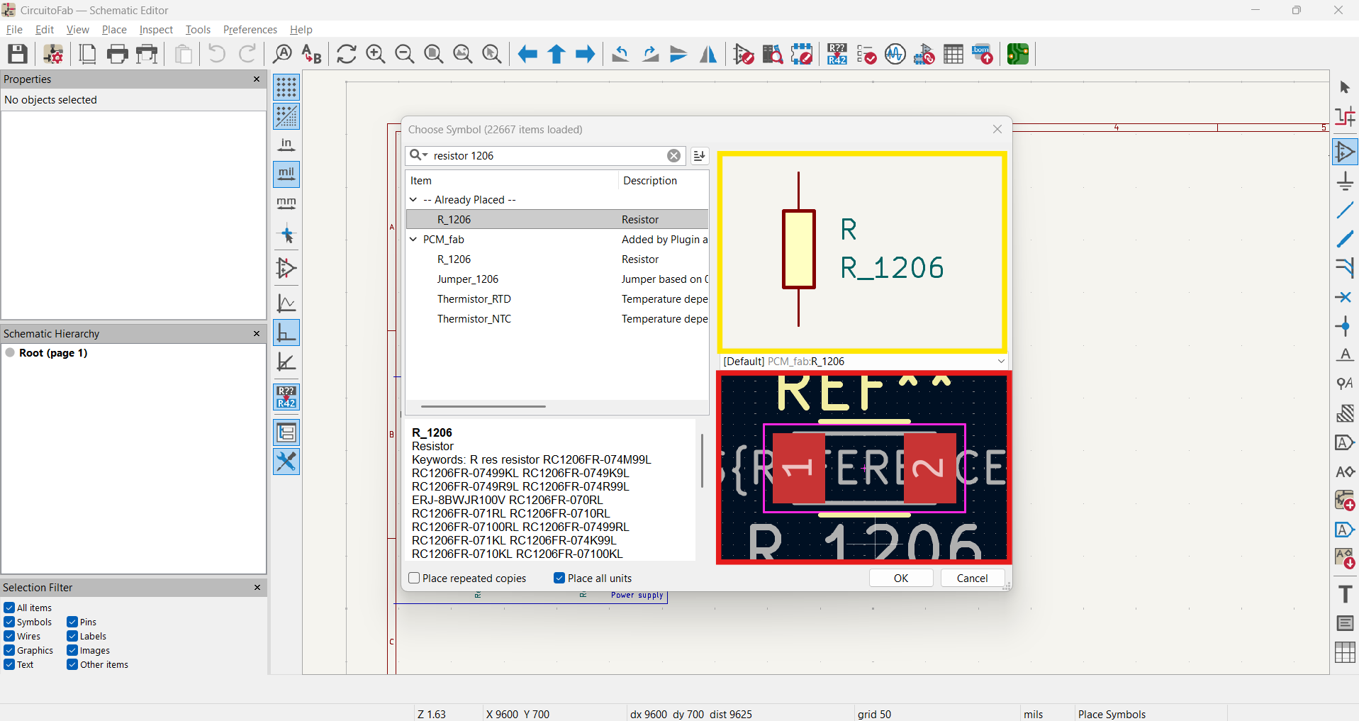
This step links the logical schematic to physical PCB components.
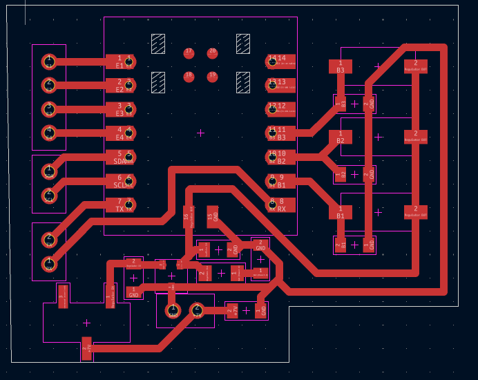
4. PCB Layout Editor
Tool Used: PCB Editor (Pcbnew)
After importing the schematic into the PCB editor, all components appeared unplaced.
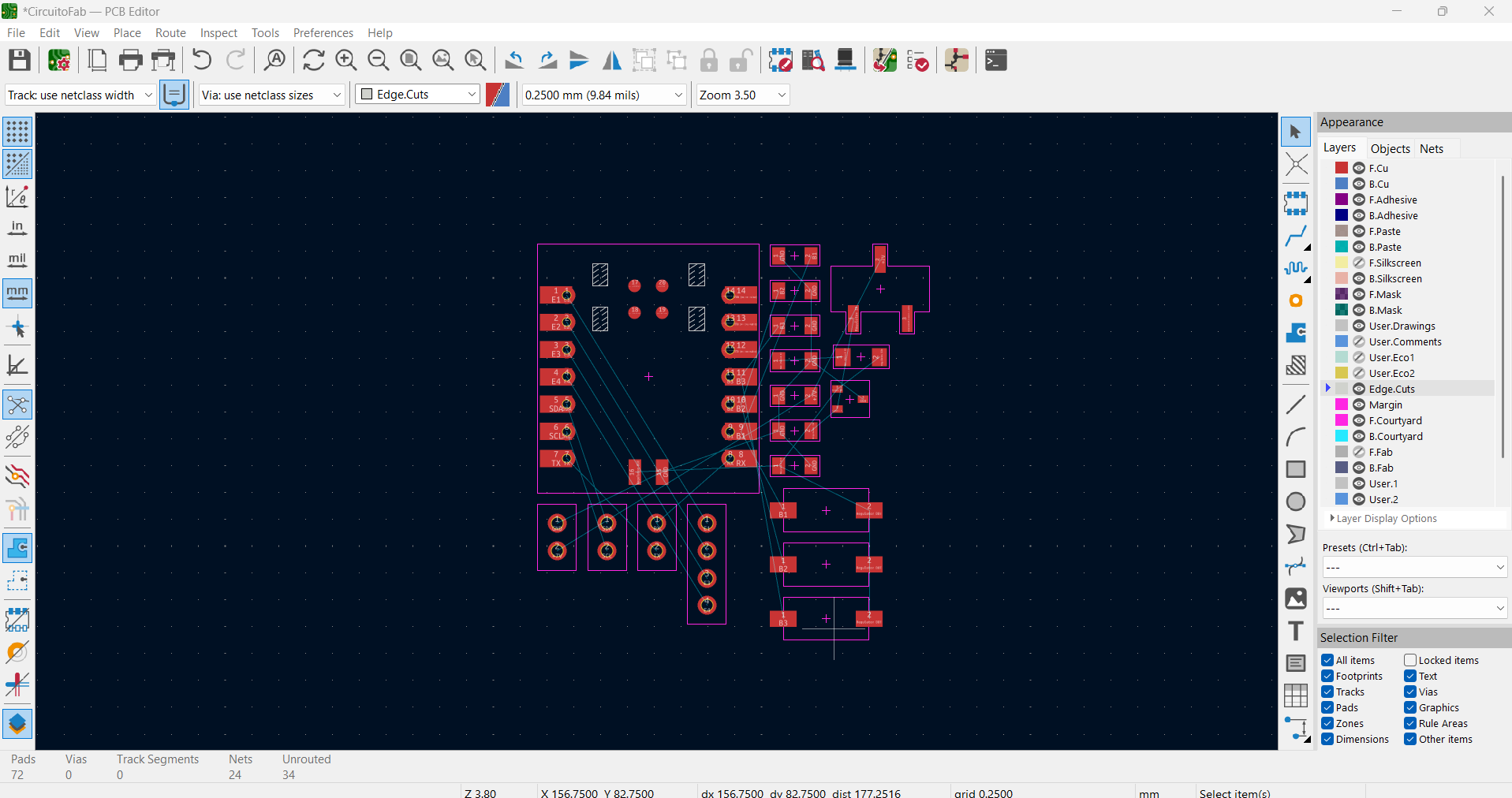
Key Steps:
- Defined board outline.
- Placed microcontroller centrally.
- Positioned regulator near power input.
- Grouped buttons logically.
- Routed power traces thicker than signal traces.
Trace routing was performed manually to maintain signal clarity and reduce noise, especially in power lines.
5. Design Rule Check (DRC)
Tool Used: Design Rule Checker
DRC verifies:
- Minimum trace width
- Clearance between traces
- Unconnected pads
- Overlap errors
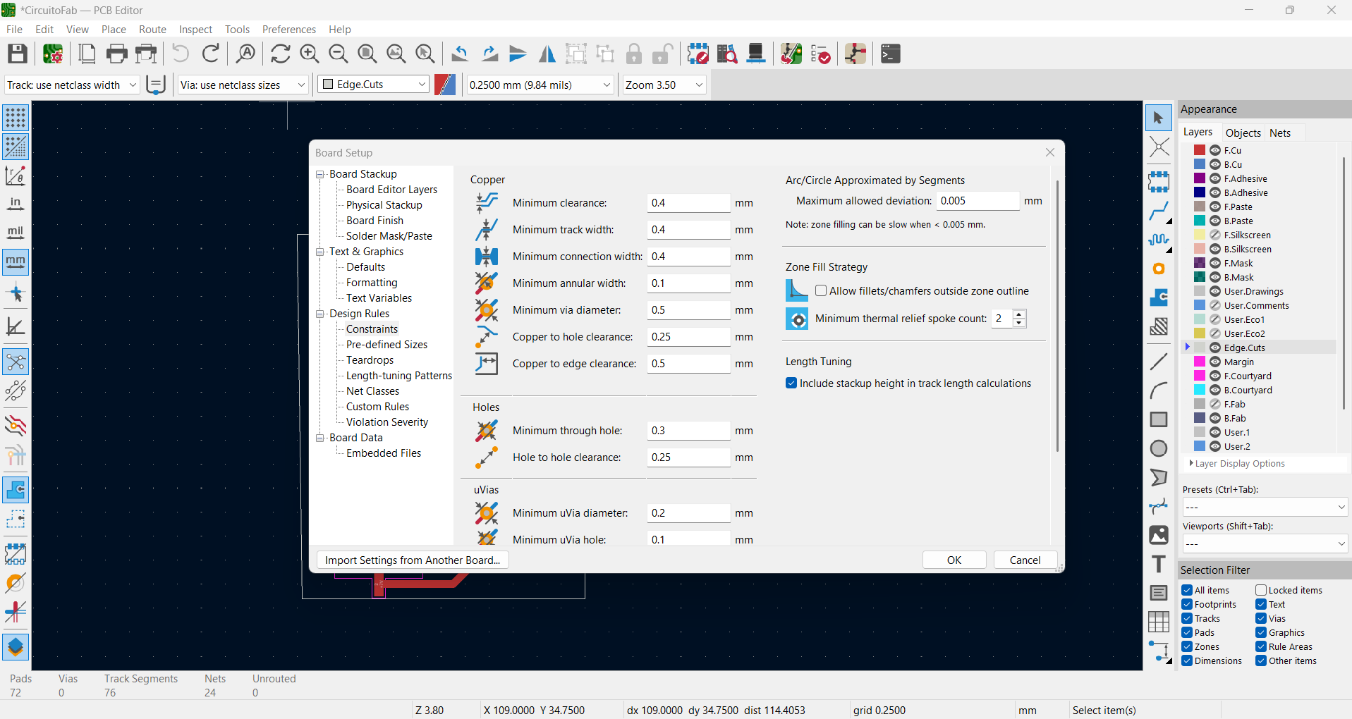
Running DRC ensured the PCB was manufacturable and electrically correct before fabrication.
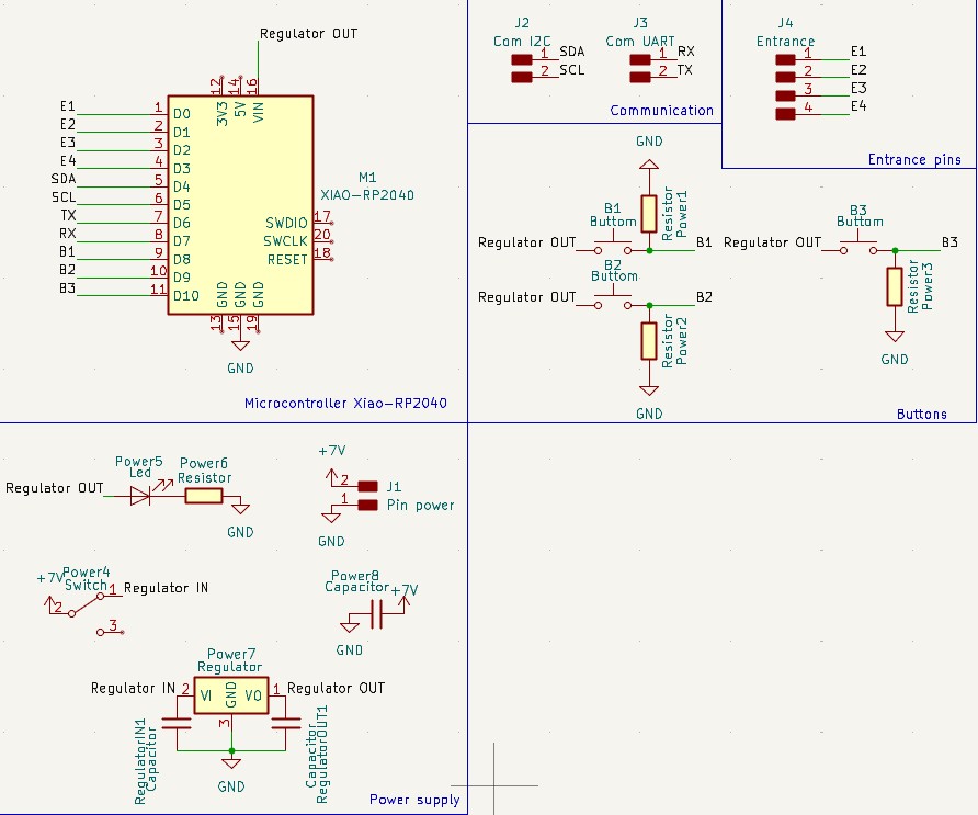
Schematic Design
System Diagram
The schematic was divided into logical blocks:
- Microcontroller (XIAO RP2040)
- Power Supply Regulation
- User Input Buttons
- Communication Headers (I2C / UART)
Layout & Component Rationale
Design Decisions
Why I Organized the Schematic in Functional Blocks
Instead of scattering components randomly, I divided the schematic into four clearly separated functional blocks. This keeps the design readable, makes debugging faster, and maps directly onto how the components are later placed on the PCB.
- Microcontroller block (top-left): the XIAO RP2040 (M1) at the center, with its pins mapped to meaningful nets — D0–D3 to the entrance pins (E1–E4), D4/D5 to I2C (SDA/SCL), D6/D7 to UART (TX/RX), and D8–D10 to the three buttons (B1–B3).
- Communication & entrance block (top-right): the I2C header (J2), UART header (J3) and the entrance pin header (J4) grouped together so all external connectors sit on one edge.
- Buttons block (middle-right): the three push buttons with their resistors.
- Power supply block (bottom-left): input connector, switch, regulator, capacitors and power LED kept isolated from the signal paths.
Grouping by function means each block can be reasoned about independently, and on the PCB I could keep the noisy power section physically away from the sensitive microcontroller signals.
Component Choices and Why
Pull-down resistors on the buttons
Each of the three buttons (B1, B2, B3) has a resistor to GND (Resistor Power1/2/3). These are pull-down resistors: when a button is not pressed, the microcontroller pin would otherwise be left "floating" and could read random highs and lows due to electrical noise. The pull-down resistor forces the pin to a defined LOW (0) state when idle, and the button pulls it HIGH only when pressed. This guarantees stable, predictable digital readings.
Capacitors around the regulator
The power supply uses two capacitors — one on the input side (RegulatorIN Capacitor) and one on the output side (RegulatorOUT Capacitor) of the voltage regulator, plus a +7V capacitor near the input connector. Their purpose is:
- Input capacitor: filters voltage spikes and noise coming from the external +7V source before it reaches the regulator.
- Output capacitor: smooths the regulated output and improves the response when the load (the microcontroller) suddenly draws more current, reducing ripple.
Power LED + series resistor
The power LED (Power5) has a series resistor (Power6) to limit the current through the LED so it isn't damaged, while giving a simple visual confirmation that the board is powered.
Voltage Regulator Configuration (from the Datasheet)
The regulator wiring — pin assignment (VI / GND / VO) and the specific input/output capacitor placement — was taken directly from the component's datasheet. Datasheets specify the recommended capacitor values and the typical application circuit for stable operation, so rather than guessing, I followed the manufacturer's reference design to guarantee the regulator behaves as intended and stays stable under load.
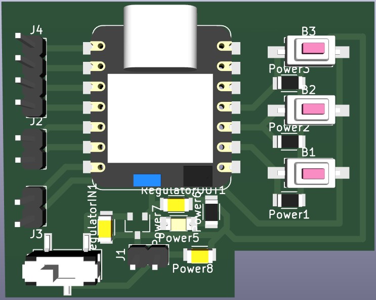
PCB Component Placement
The placement on the PCB mirrors the schematic blocks:
- XIAO RP2040 centered: placed in the middle so its many connections can fan out symmetrically to every block, keeping trace lengths short.
- Connectors on the edges: the entrance pins (E1–E4), I2C and UART headers were placed along the left edge for easy external access.
- Buttons grouped on the right: the three buttons and their pull-down resistors sit together, matching their schematic block.
- Power section at the bottom: regulator, capacitors and input placed near the power input, isolated from signal routing.
- Thicker GND / power traces: power and ground traces were routed wider than signal traces to carry more current safely and reduce voltage drop and noise.
Verification: ERC and DRC
Electrical Rules Check (ERC) — at the schematic stage
Before moving to the PCB, I ran the Electrical Rules Check in the schematic editor. ERC analyzes the logical connections and flags electrical problems such as floating (unconnected) pins, power inputs that aren't driven by any power source, and conflicting outputs. This is what caught issues like a pin left without a net or a missing power connection, so I could fix them before they became physical mistakes on the board.
Design Rule Check (DRC) — at the PCB stage
Once the board was routed, I ran the Design Rule Check in the PCB editor. DRC verifies that the physical layout is actually manufacturable by checking minimum trace width, clearance between traces, unconnected pads, and overlaps. Passing DRC confirmed that no two traces were too close together and that every net in the schematic was fully routed on the board.
Together, ERC and DRC act as two safety gates: ERC makes sure the circuit is electrically correct, and DRC makes sure it is physically buildable — both passing before generating the fabrication files.
Microcontroller
Core Control
XIAO RP2040
The XIAO RP2040 was selected because it provides:
- Dual-core ARM Cortex-M0+
- Compact footprint
- Multiple communication protocols (I2C, SPI, UART)
- PWM support for motor and servo control
The board connects:
- Digital inputs (Buttons B1, B2, B3)
- I2C header for expansion
- UART header for debugging
- External regulated power input
Power System
Regulation
Voltage Regulation
The board includes a voltage regulator to convert +7V input into a stable regulated output suitable for the microcontroller.
- Input: +7V external source
- Voltage regulator with input/output capacitors
- Power LED indicator
- On/Off switch
Capacitors were included on both input and output sides of the regulator to ensure voltage stability and reduce ripple.
| Component | Purpose |
|---|---|
| Regulator | Voltage stabilization |
| Input Capacitor | Filter voltage spikes |
| Output Capacitor | Improve load response |
| Power LED | Visual power indication |
Input Interface
Buttons
Push Buttons
Three push buttons were integrated for user interaction. Each button includes a resistor for pull-down configuration to ensure stable logic levels.
- B1 – Primary input
- B2 – Secondary input
- B3 – Auxiliary control
The design ensures noise reduction and stable digital readings.
Communication
I2C / UART
Communication headers were added to allow:
- I2C peripheral expansion
- UART debugging
- Future sensor integration
This modular approach allows the board to scale with the final project.
Final Project Integration
This electronic design forms the core control board of my final project. It centralizes power regulation, user interaction, and communication into a compact PCB architecture.
The modular design ensures adaptability and future expandability.