Electronics Production
During the group assignment, we learned to master the PCB production process by evaluating and comparing two different manufacturing methods: mechanical milling with the Roland MonoFab SRM-20 and laser ablation with the xTool F1 Ultra. We performed minimum clearance and trace width tests on both machines to establish specific design rules, tolerances, and optimal parameters such as depth of cut, feed rate, laser power, and speed necessary for reliable circuit manufacturing.
Regarding machine safety and operation, we learned to generate toolpaths using Mods and to configure them precisely. Furthermore, we complemented our practical manufacturing skills by learning to export Gerber files and configure manufacturing parameters to outsource PCB production through a commercial board manufacturing company like JLCPCB.
Group Assignment Week 8
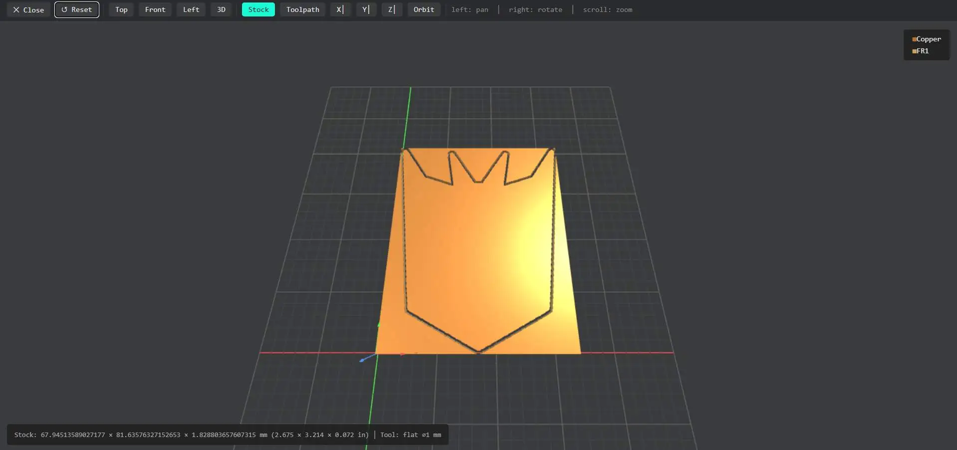
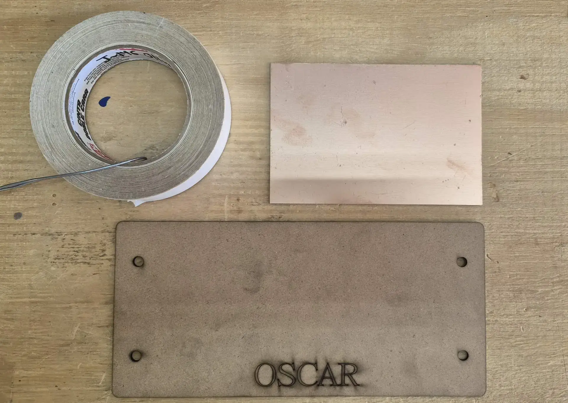
For my assignment, I fabricated the multipurpose board I originally designed during week 6. I chose the Roland MonoFab SRM-20 machine for its ease of use and robust construction for PCB fabrication. Unlike a laser machine, the SRM-20 offers a comprehensive solution that allows all the necessary steps to be performed on a single machine: surface-mount milling, hole drilling, and board contour cutting.
Electronic Design
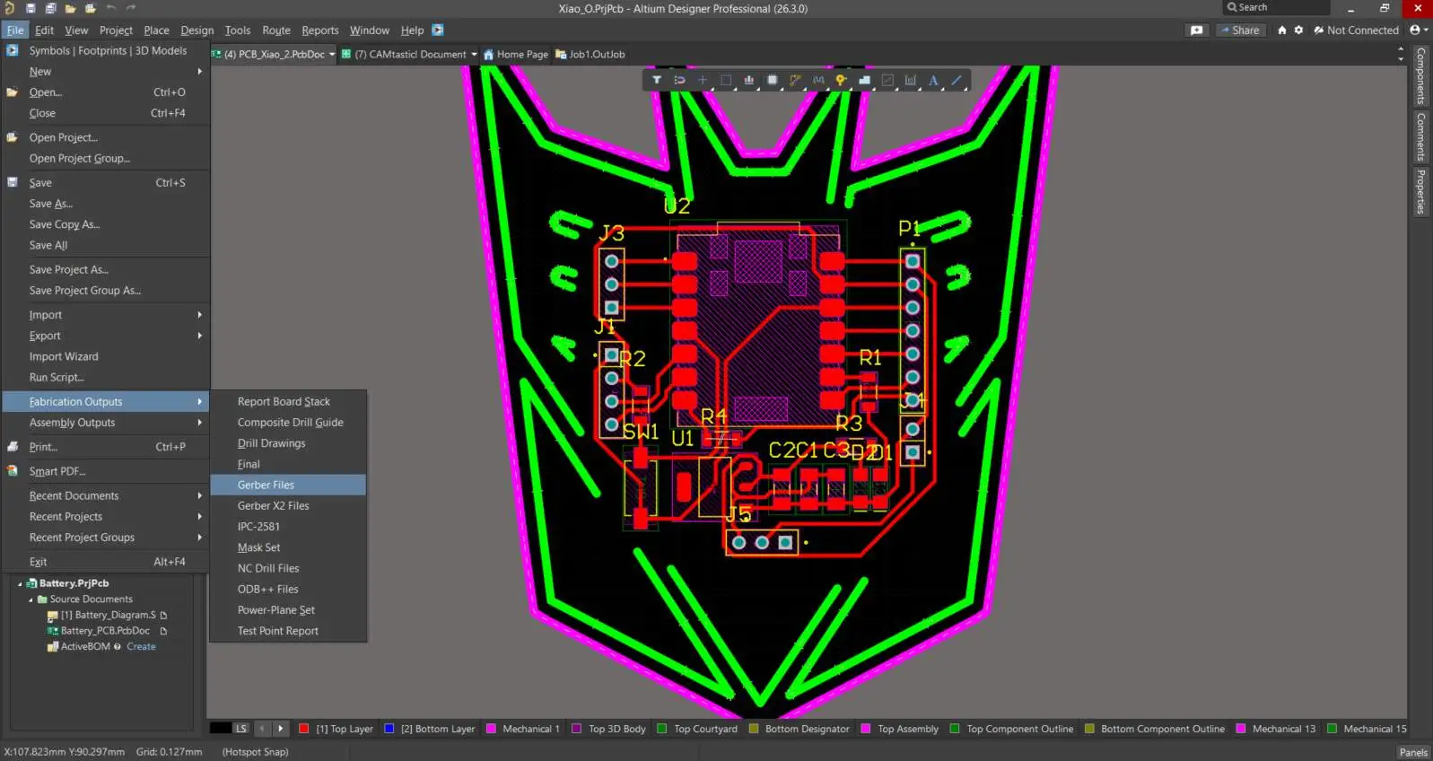
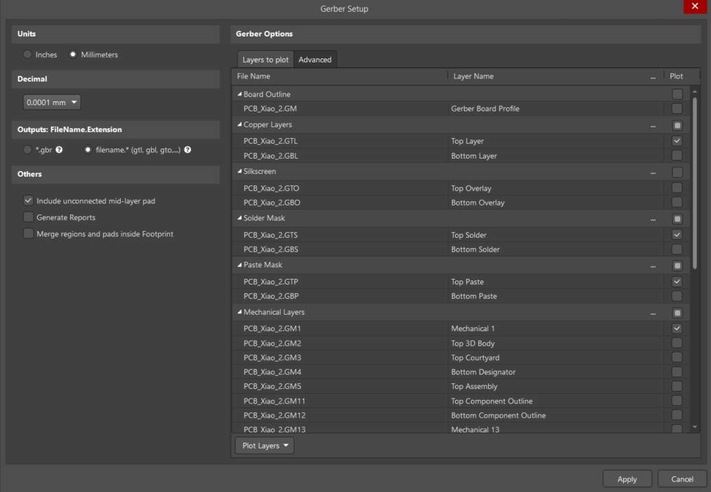
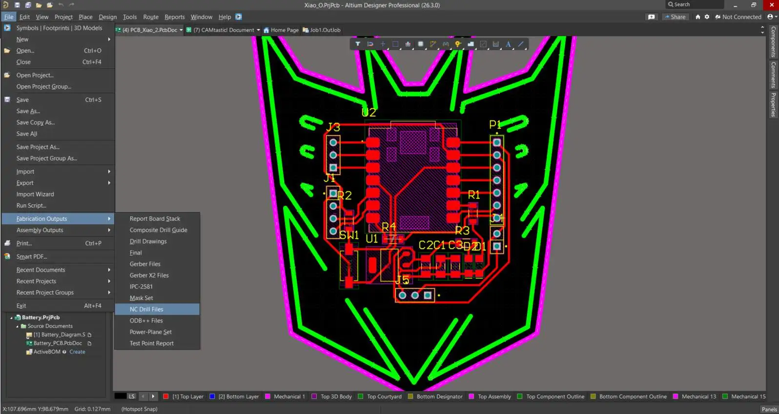
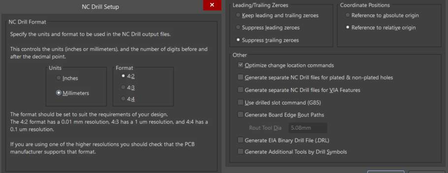
Outputs Gerber
To generate the manufacturing files for PCB production in Altium Designer, the board design must be exported as Gerber files. We then use the Gerber2PNG platform to convert these files into high-resolution PNG images. Finally, these images are imported into Mods to calculate and generate the toolpaths (.rml) for the Roland MonoFab.
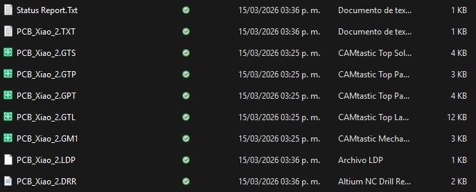
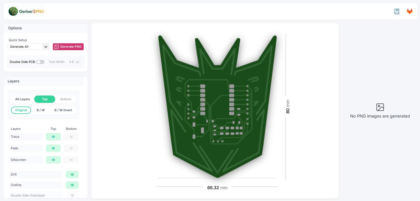
PNG Images Exported

Mods CE
Mods Community Edition is a powerful, node-based web tool used to convert our design images into machine instructions. While the platform offers a wide variety of programs for different fabrication processes and machines, we need a specific workflow for our board.
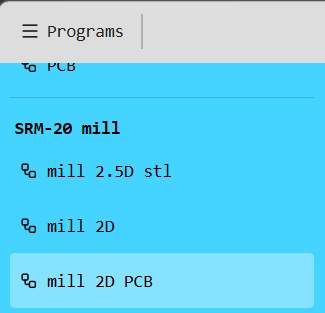
As shown in the image, we navigate to the SRM-20 mill category and select the mill 2D PCB program. This automatically sets up the ideal node environment for calculating the toolpaths required to mill printed circuit boards.
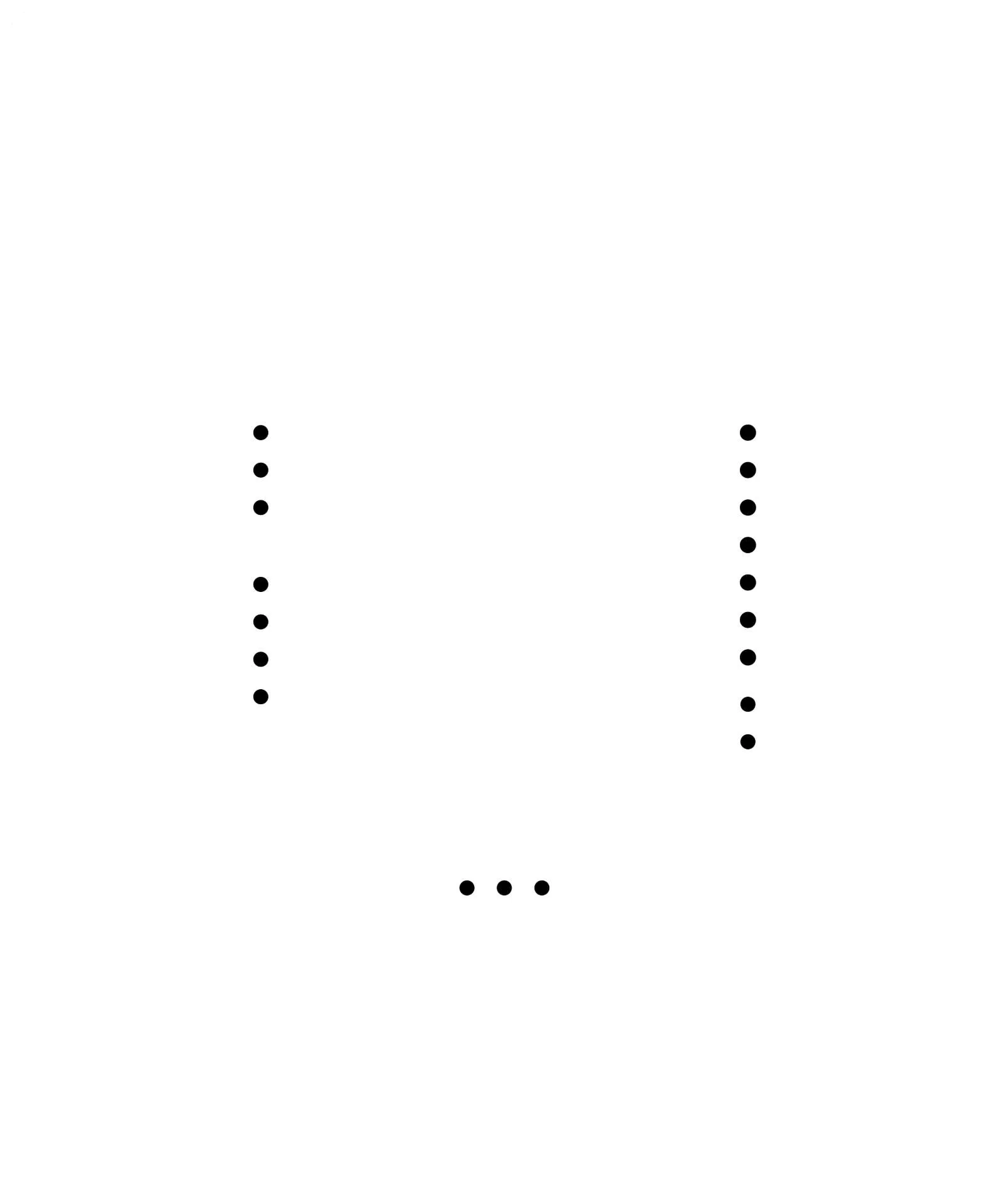
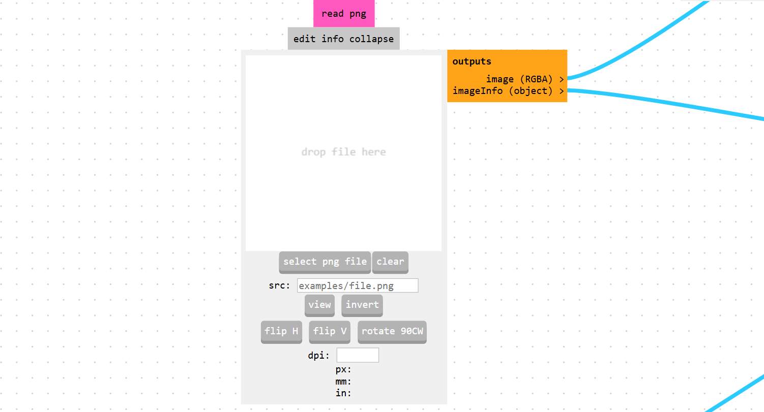
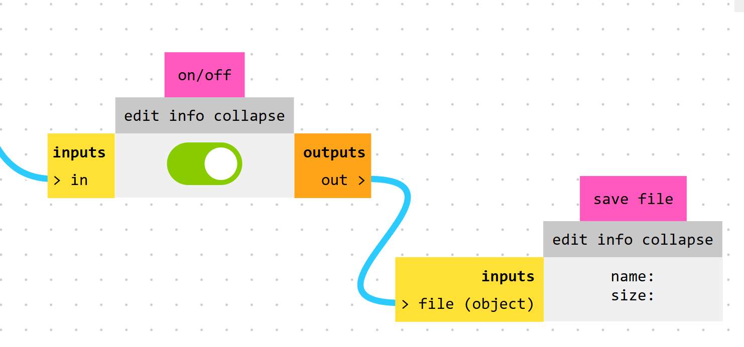
Once the SRM-20 workspace is loaded, the first step is to import our design using the Read PNG node. By clicking Select PNG file, we upload the monochrome images we previously generated with Gerber2PNG.
 Beam
Beam
 Traces
 Borders
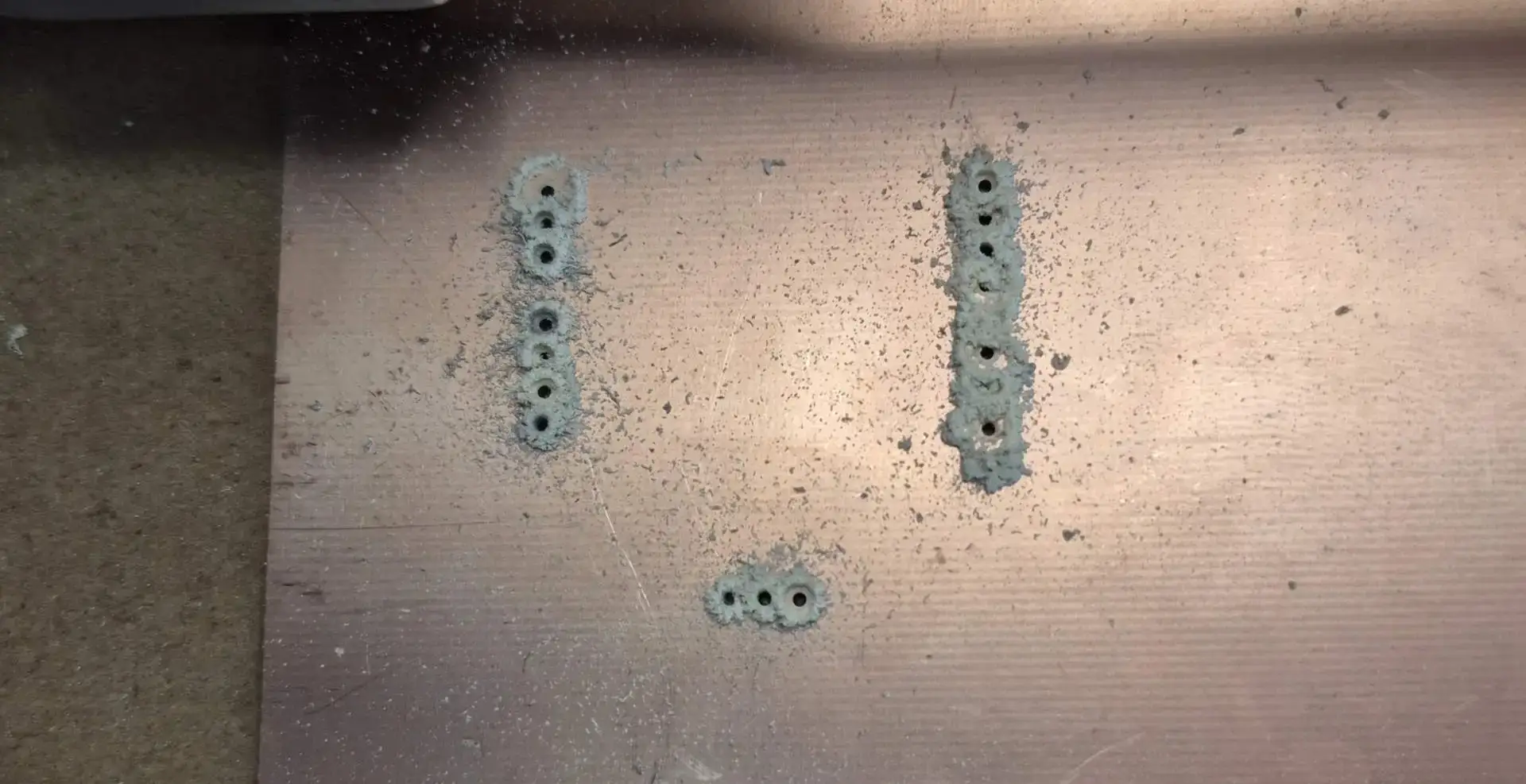
The first step in the machining process is drilling the holes. I did this first to prevent the copper from breaking, which often happens if the drill bit hits the board after the traces have already been milled.
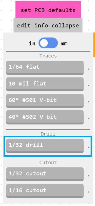
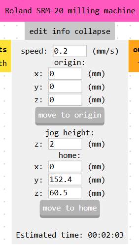
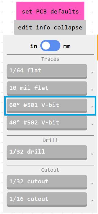
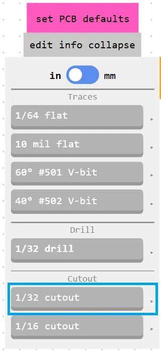
After loading the image of the holes, I went to the Set PCB Defaults node and selected the Contour Mill (1/32) option to pre-configure the tool for drilling. In the milling parameters, I verified the tool diameter of 0.0312 inches (1/32 in.) and used a depth of cut of 0.6 in. with a maximum depth of 0.072 in. to ensure the drill bit completely drilled through the board in multiple passes. Finally, in the machine control node, I set the cutting speed to 0.2 mm/s and ensured that all origin coordinates (X, Y, Z) were strictly set to 0.
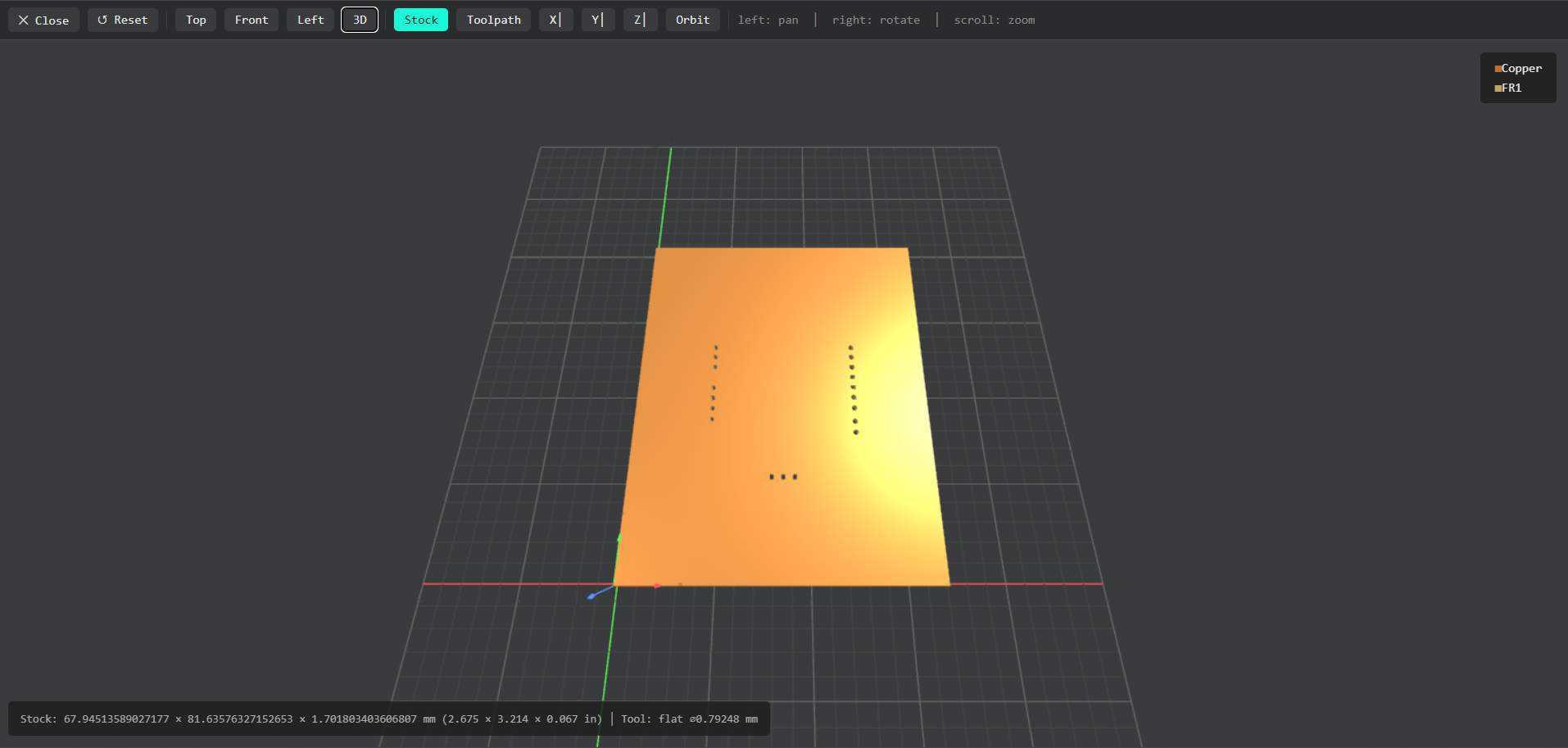
Clicking Calculate opens a tab with a 3D preview of the calculated process, helping to visualize what the machine will do.
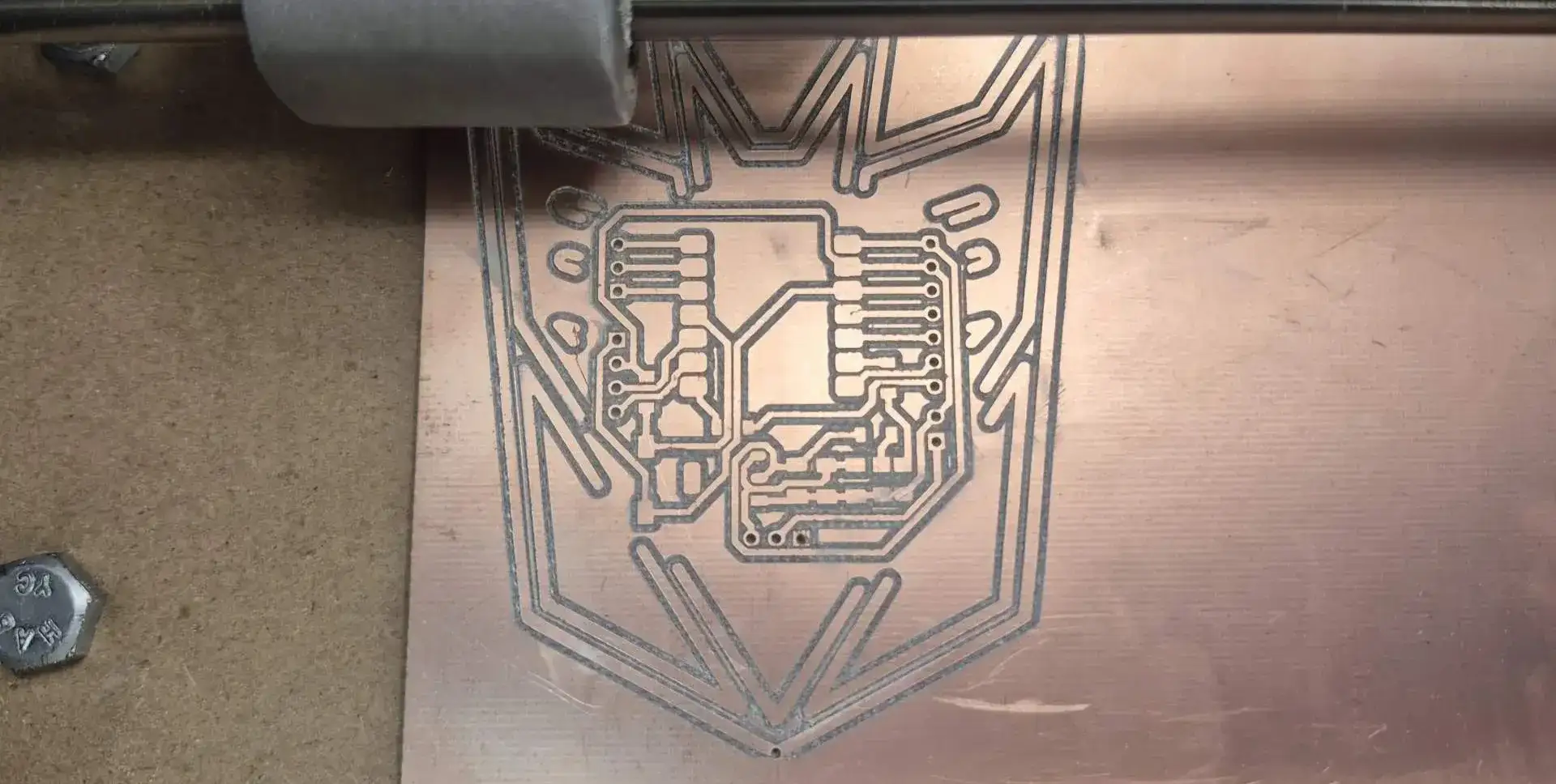
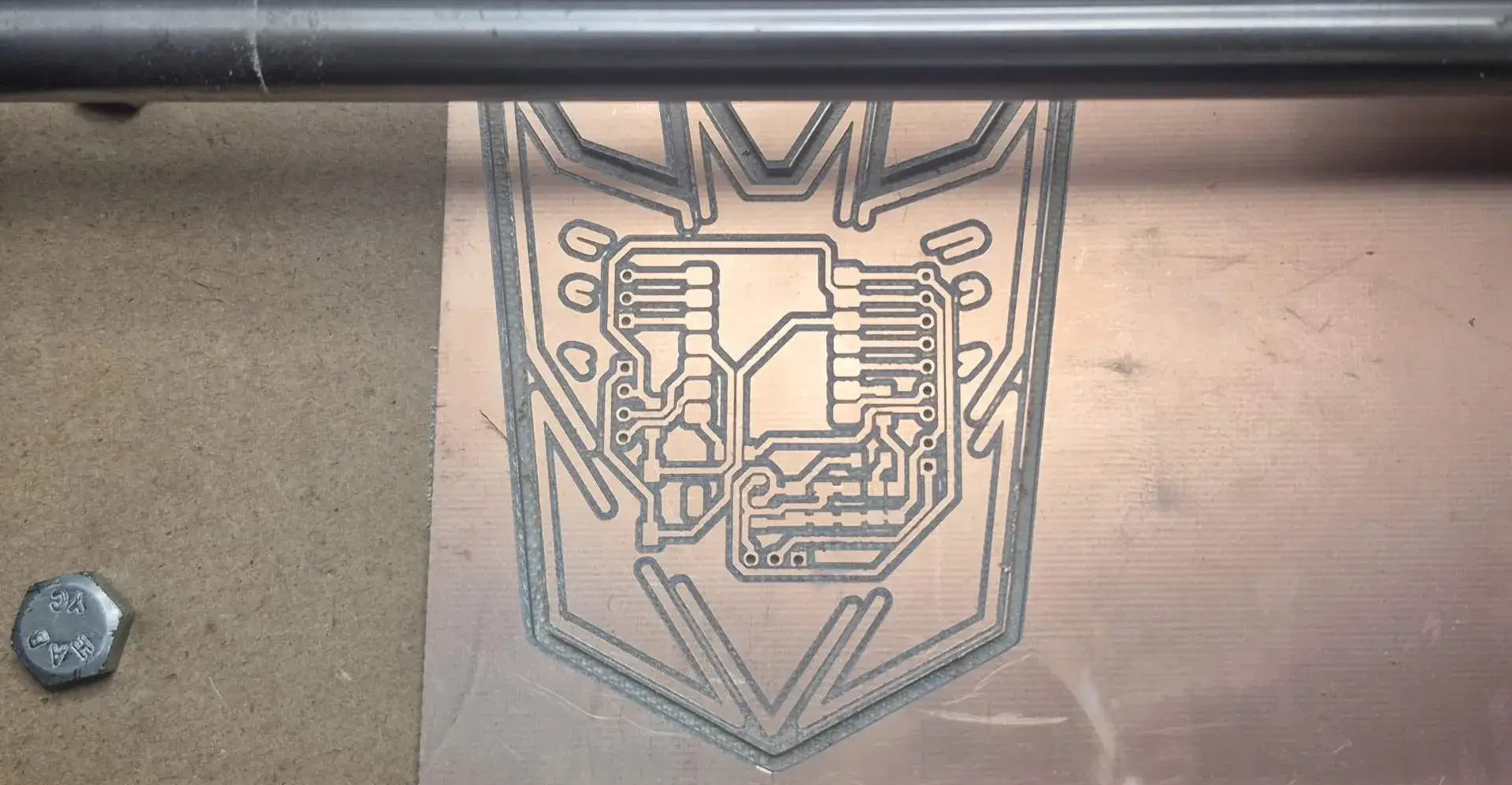
With the holes drilled, the next step is milling the circuit's traces.
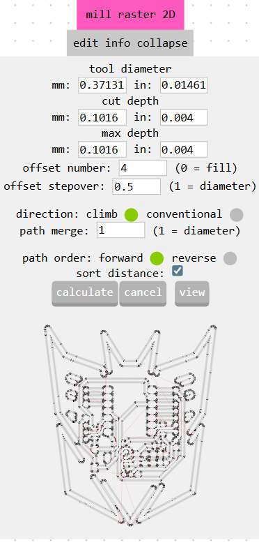
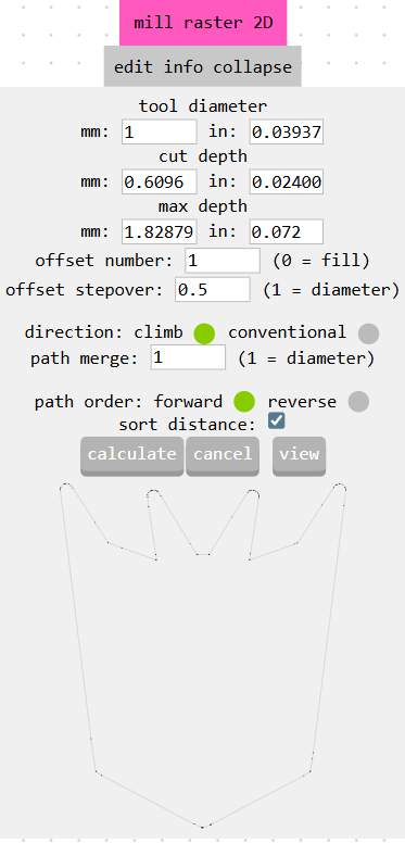
For the trace milling operation, I configured the settings to use a 60° V-shaped drill tool, which provides excellent accuracy for creating fine copper traces. In the machine control node, I set the cutting speed to 4 mm/s and a 4 offset to ensure no unwanted parts remain attached. Finally, I verified that all origin coordinates were strictly set to 0.
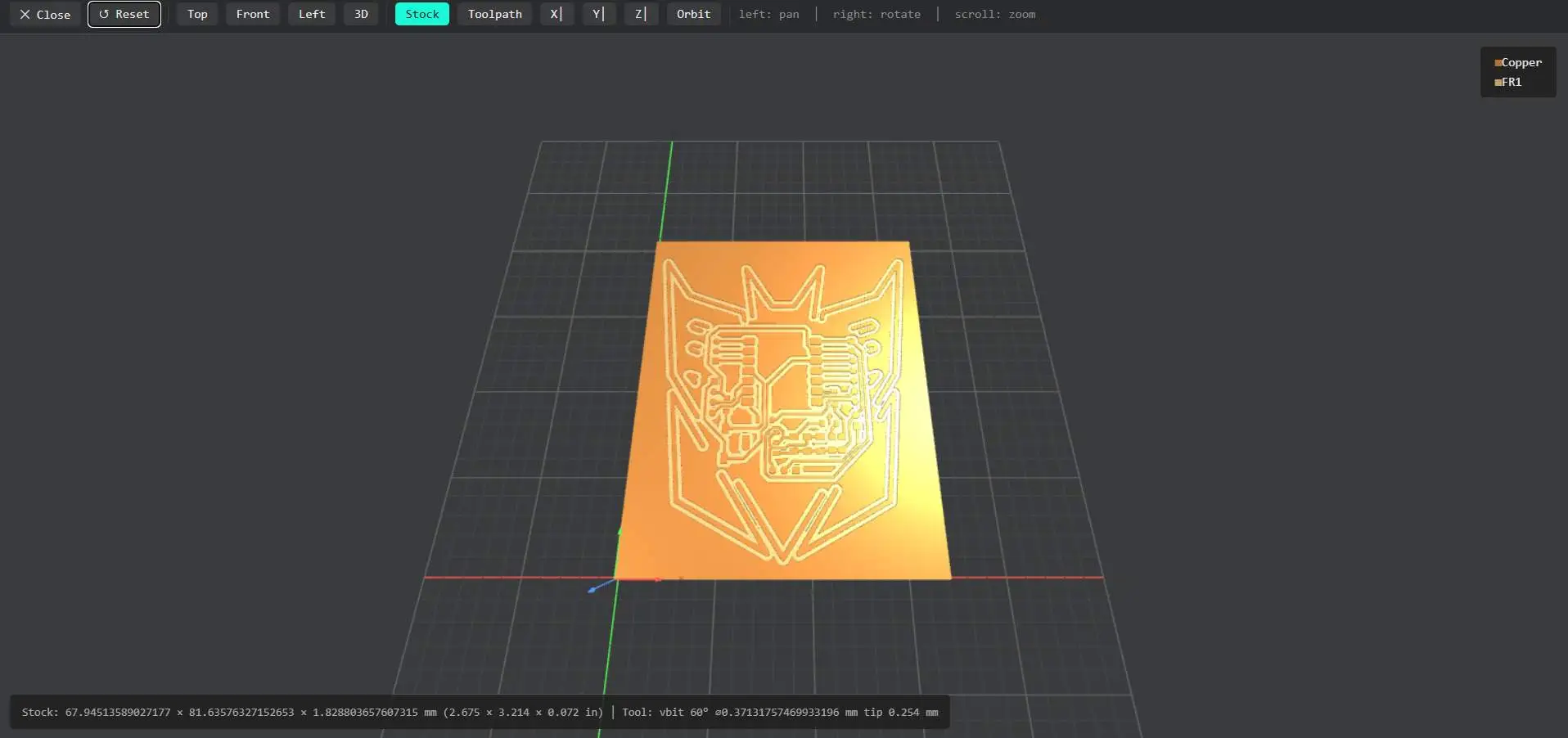
Once the traces are etched and the holes drilled, the final step is to generate the toolpath for the board outline. This cutting process separates our finished circuit from the main copper board.
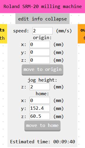
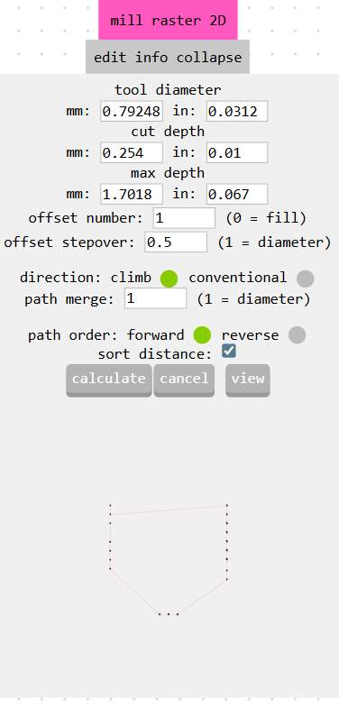
For the final step, cutting the board's exterior outline, I configured the settings to use a 1/32 inch end mill. In the mill raster 2D parameters, the tool diameter was set to 1 mm, with a cut depth of 0.024 in and a max depth of 0.072 in, ensuring the machine cuts safely through the FR4 material in multiple passes. I kept the offset number at 1 for a single contour cut. Finally, in the machine control node, I set the cutting speed to 2 mm/s.
A crucial step before running the calculation is to ensure the Save File node is active and connected. This is mandatory, as it instructs the software to generate and download the final file (.rml) to your computer. This generated file contains all the G-code instructions and coordinates that the Roland MonoFab machine needs to physically perform the calculation.
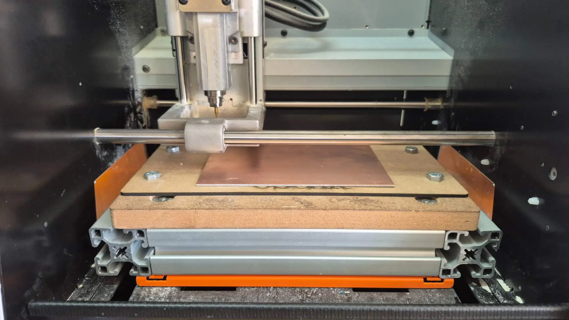
Machining Process
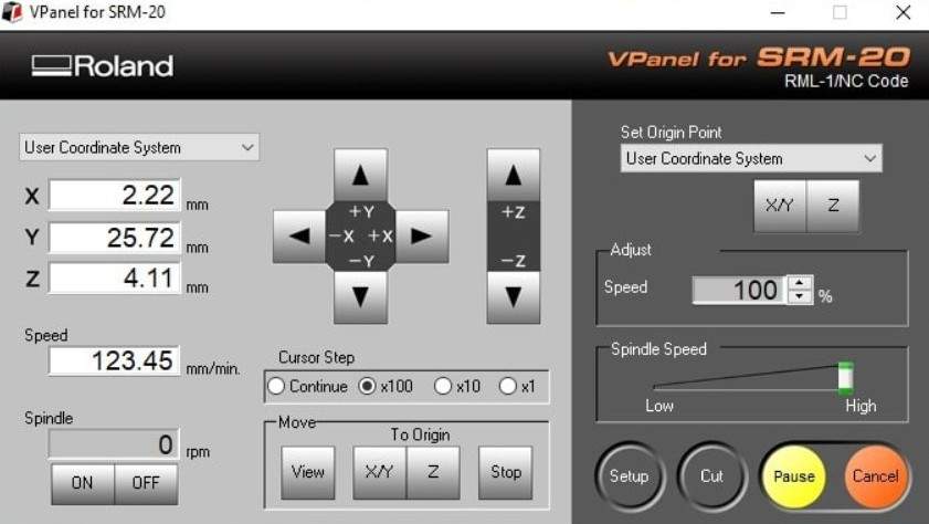
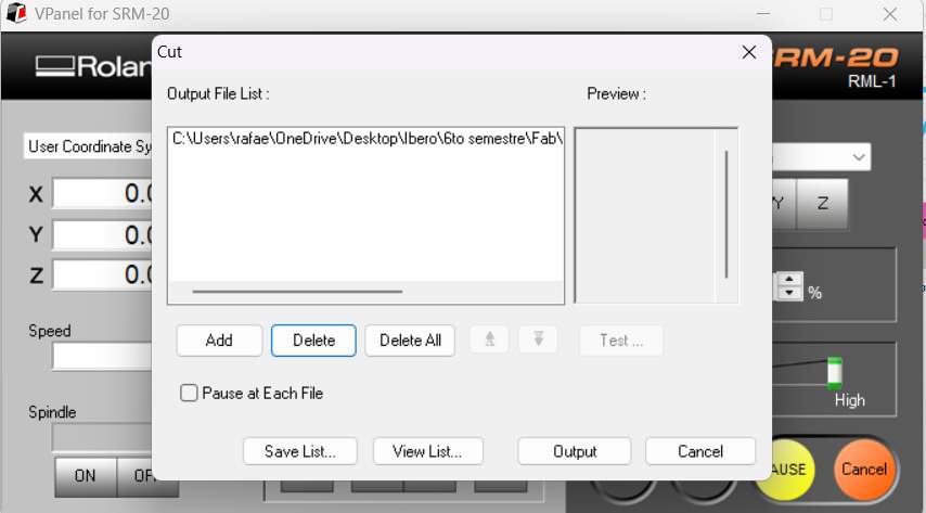
To physically mill the board, I used the VPanel software for SRM-20. First, I manually set the X, Y, and Z origin points on the copper board. Then, in the "Cut" menu, I loaded the generated .rml file and pressed "Output" to start the machine.
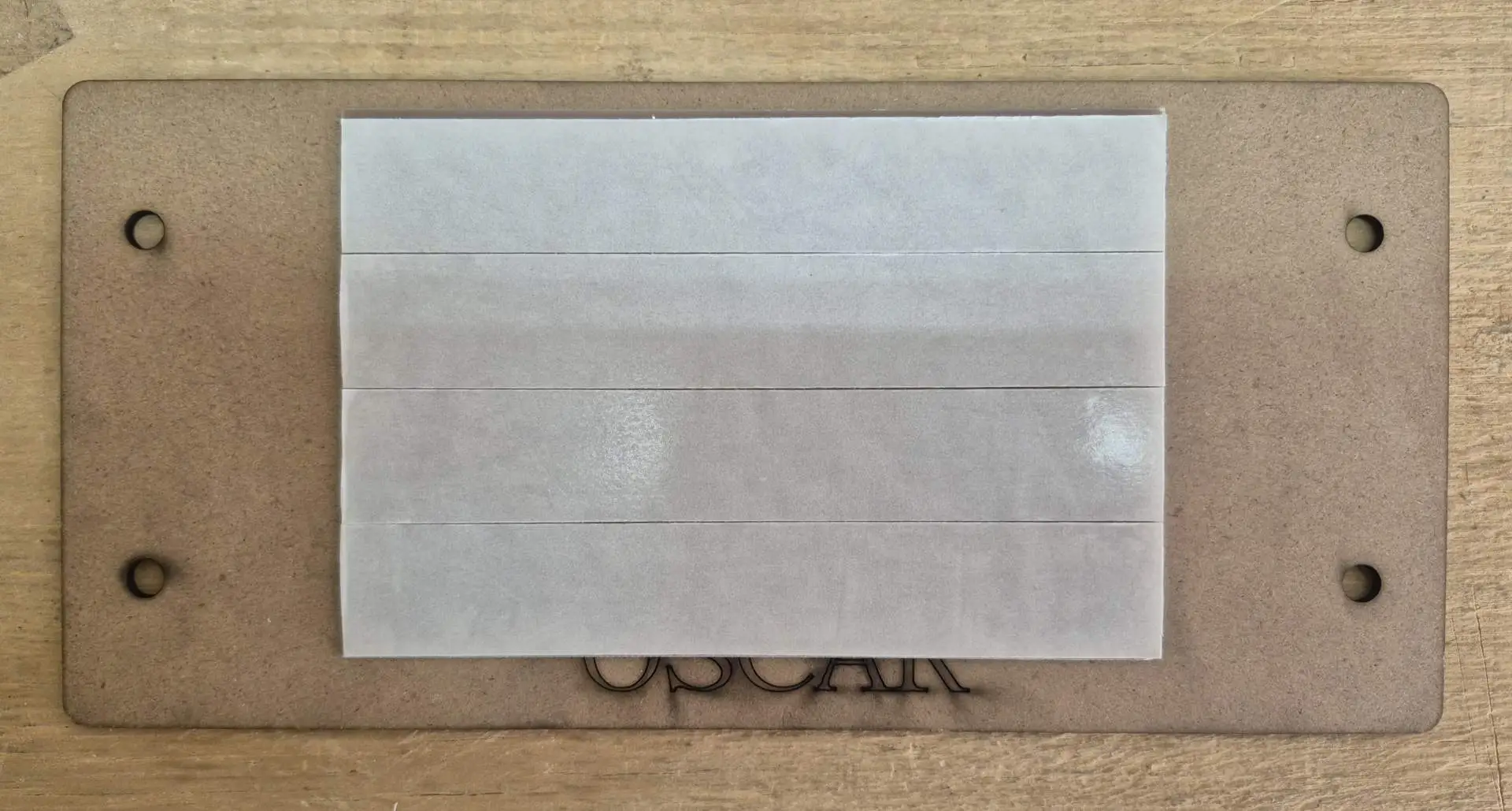
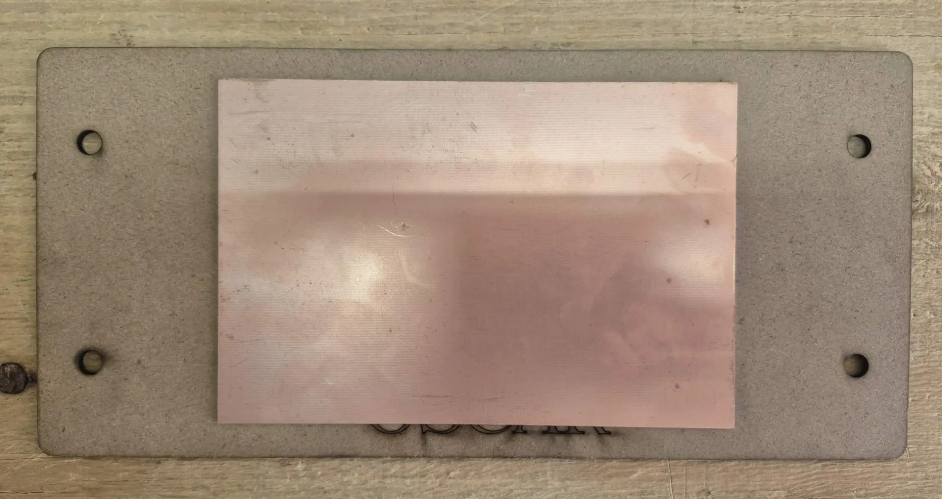
For manufacturing, we use an uncoated copper plate. To secure it to the machine and prevent vibrations from damaging the cut, it is essential to use double-sided adhesive tape, applied evenly to the back.
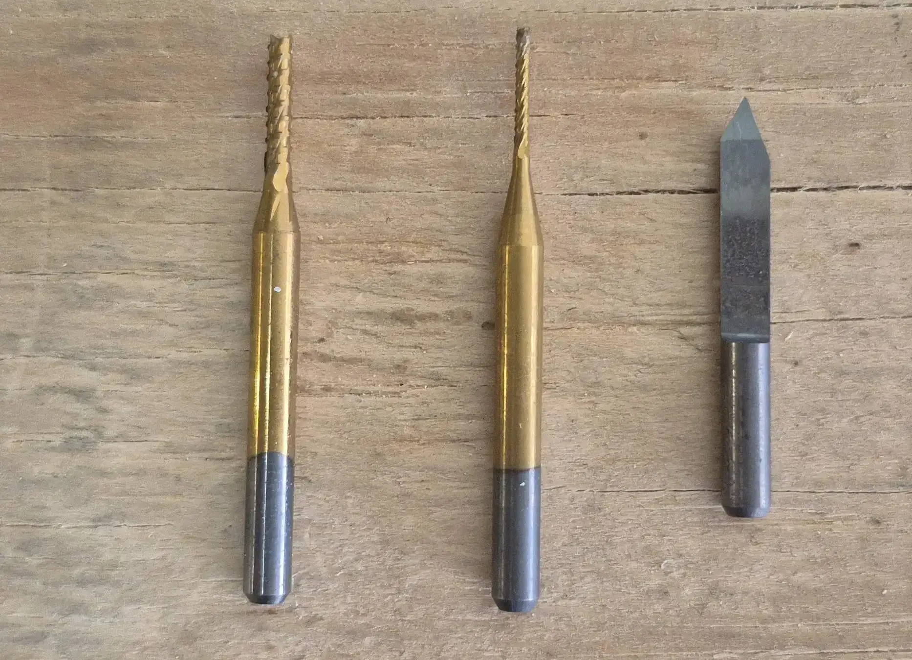
I used the 60° V-shaped bit for fine line engraving, the 1/32" flat end mill for the holes, and a 1 mm end mill for the outer contour.
I firmly attached the copper plate to the sacrificial base with double-sided tape. It's crucial to press down firmly to ensure it's completely flat, guaranteeing accurate Z-axis adjustment across the entire work area.
To secure the copper board inside the MonoFab, I placed it on the machining bed and carefully tightened the nuts at all four corners. It's crucial to tighten them evenly to ensure the board remains perfectly flat and level. Any warping or tilting can cause the milling cutter to cut too deeply in some areas and not reach the copper in others, thus ruining the fine traces.
Drilling Machining
Traces Milling
Board Cutting
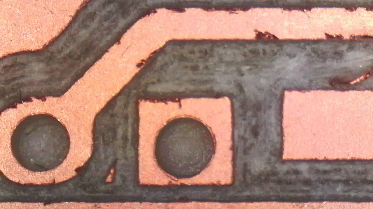
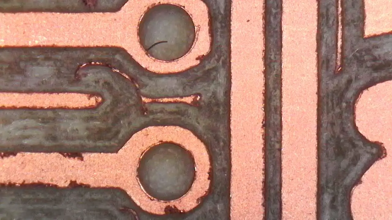
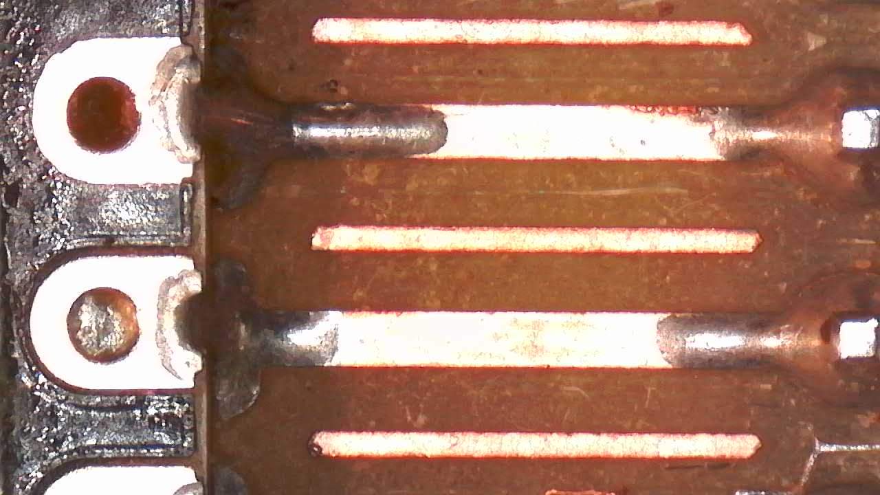
Final Result of the Machining
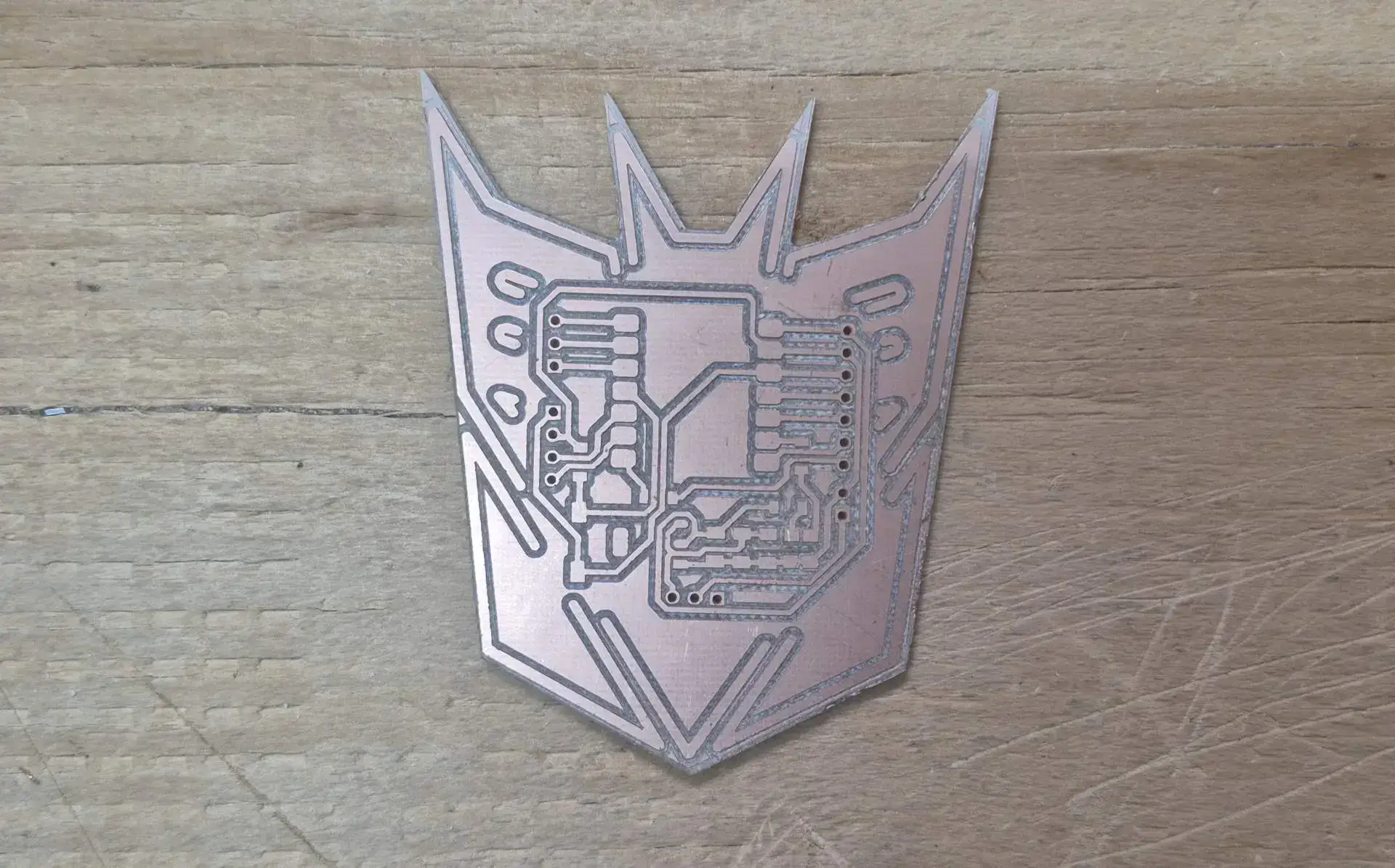
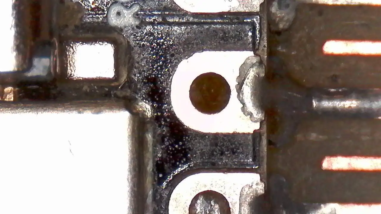
I used a digital microscope to be able to take highly detailed captures of the result of the machining.
Components Welding Process
Once the PCB has been machined, the next important phase in the manufacturing process is the assembly of the electronic components. Since our board is designed with SMD components, a fine-tipped soldering iron and tweezers are required to carefully place and solder each component onto its corresponding copper pads. Proper lighting ensures high-quality soldering.
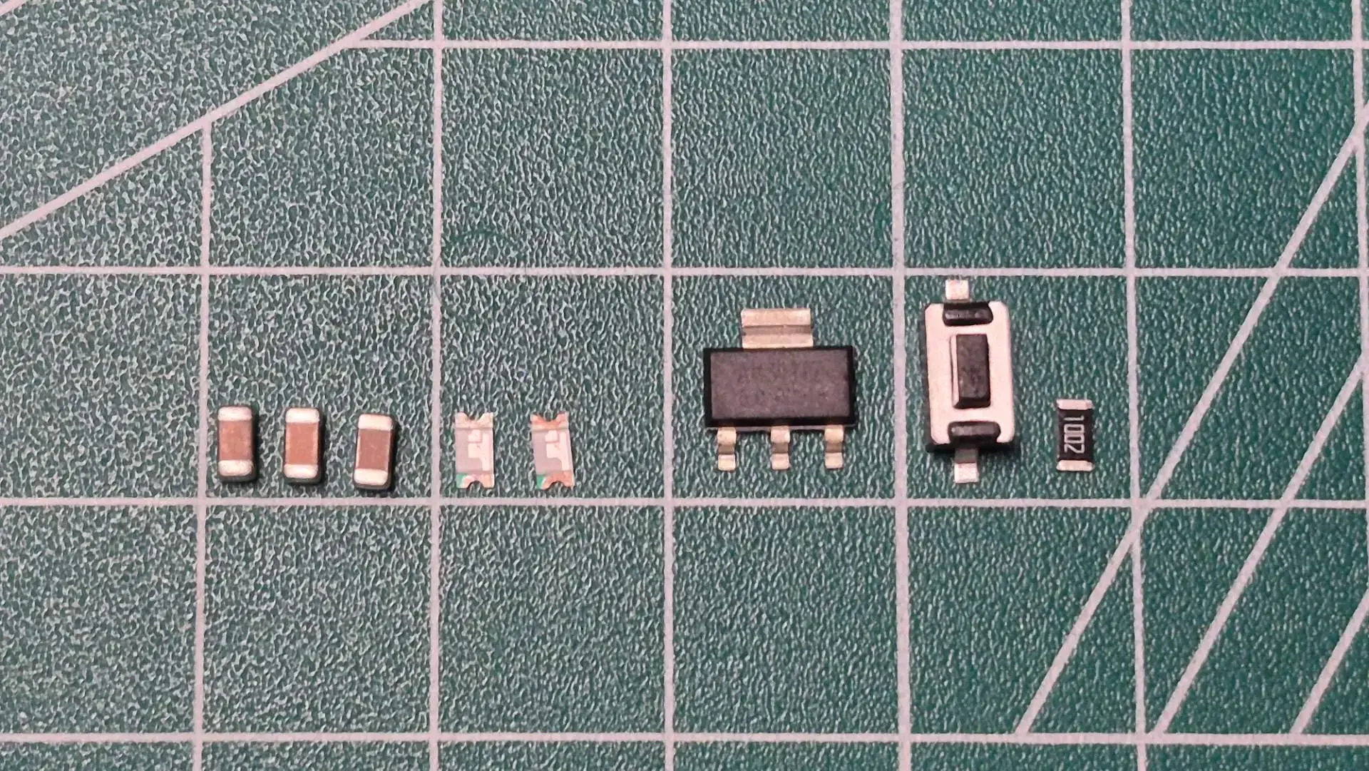
SMD Components
- 1x Seeed Studio XIAO RP2350
- 1x 5V AMS1117 SMD Voltage Regulator
- 3x 10uF SMD Capacitors
- 1x SMD Red LED
- 1x SMD Blue LED
- 2x SMD Resistors Current limiting for LEDs (180Ω and 270Ω)
- 1x SMD Push Button
- 1x SMD Resistor for the button circuit (10kΩ)
- 1x Male Header Pins
To calculate the resistances of my LEDs, I used the following calculations:
Rlr = (3.3V - 1.8V) / 5mA Rlr = 300Ω but since 300Ω is not a standard value, I used a 270Ω resistor for the red LED.
Rlb = (5V - 3.6V) / 10mA Rlb = 140Ω but since 140Ω is not a standard value, I used a 180Ω resistor for the blue LED.
It is important to note that although the original board was designed around the Seeed Studio XIAO ESP32C3, I used the newer XIAO RP2350 for this build. Fortunately, the entire XIAO microcontroller family shares a standardized form factor and pinout. This means that the power pins (5V, 3.3V, GND) and the general-purpose input/output (GPIO) pins are located in the exact same physical positions. Because of this, the RP2350 is fully compatible and serves as a perfect drop-in replacement without needing any modifications to the milled copper traces.
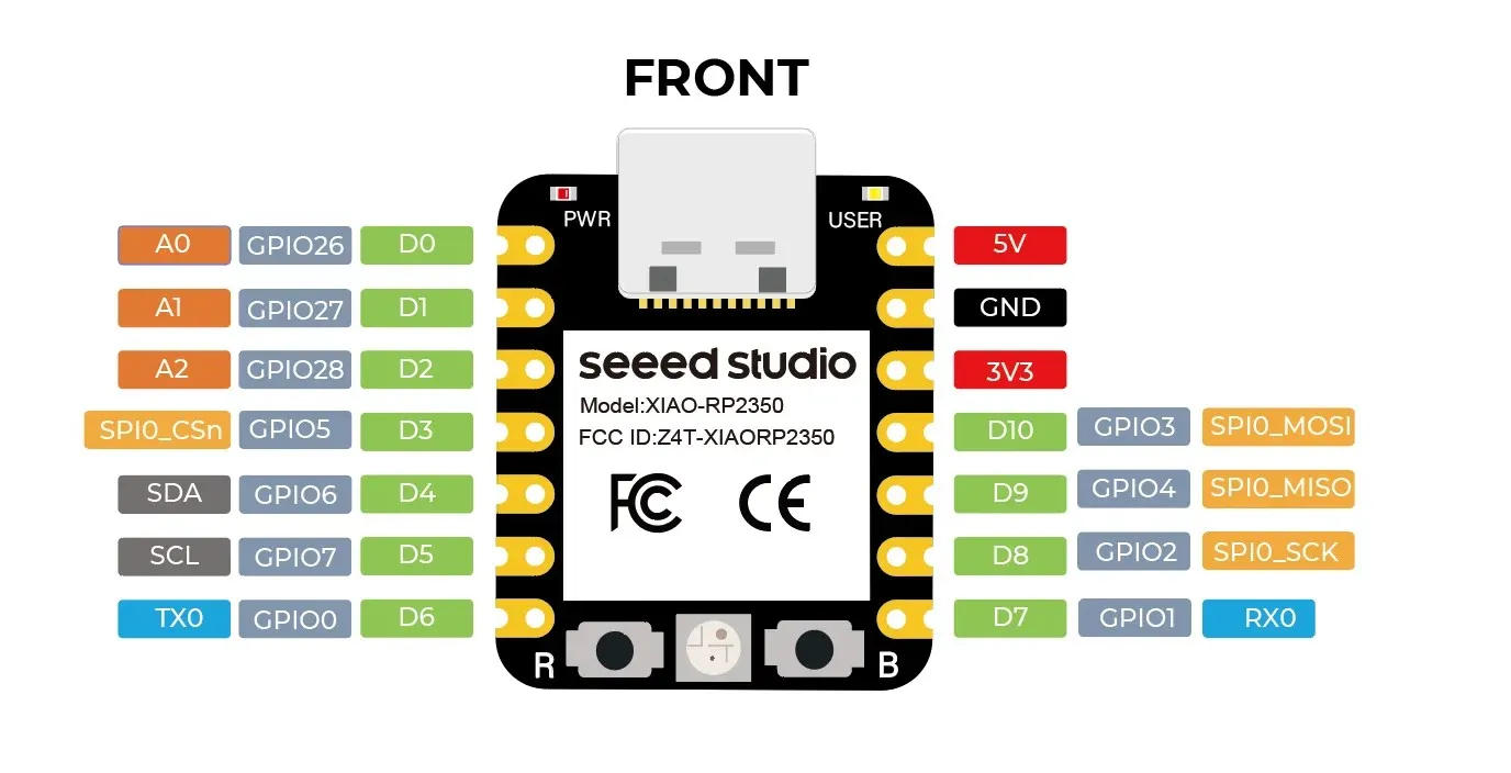
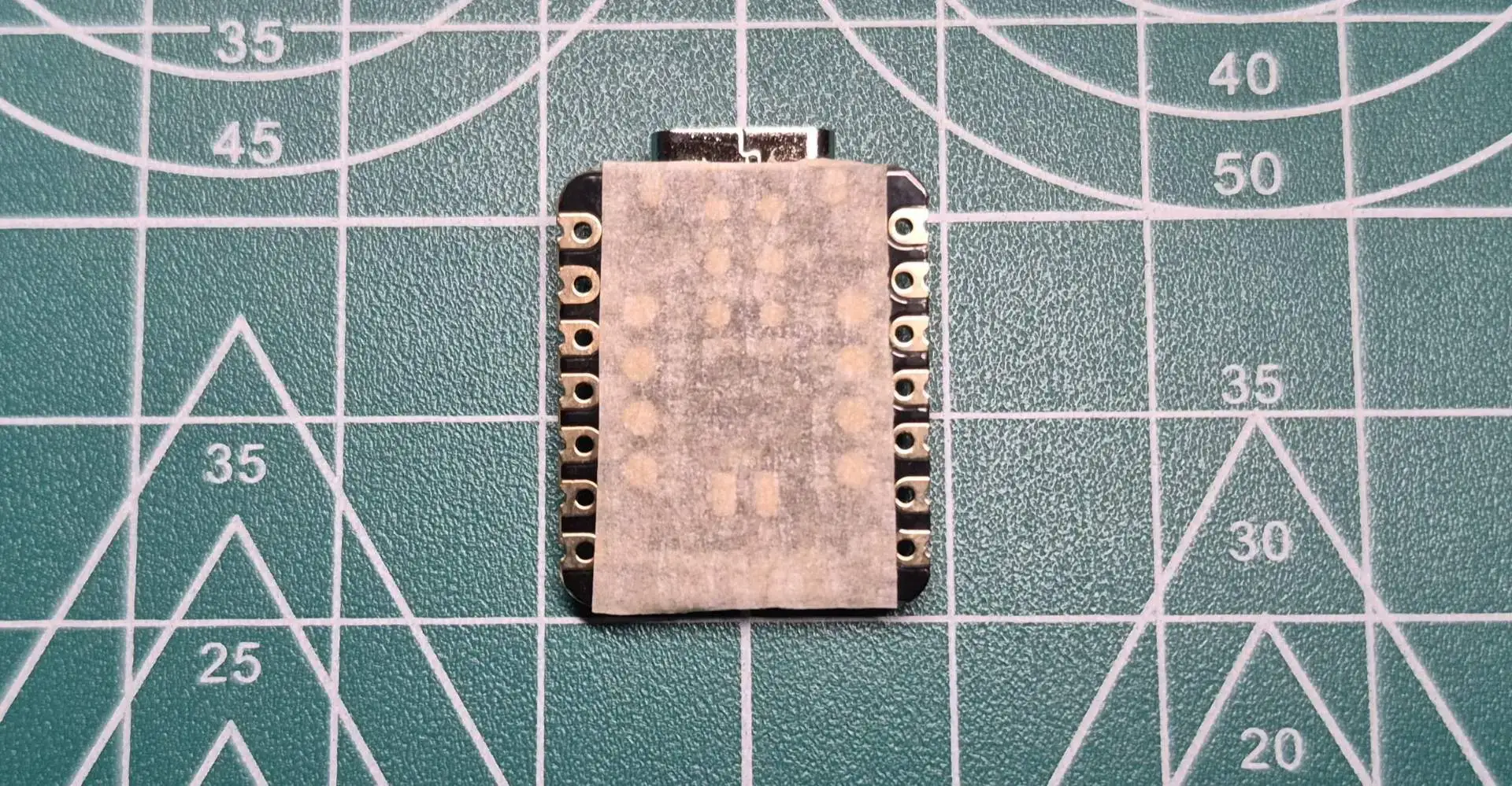
A crucial step before soldering the microcontroller is to insulate its underside. The Seeed Studio XIAO RP2350 has several exposed test pads on its underside. To prevent these pads from accidentally making contact and short-circuiting the copper traces on our board, I applied tape to the back of the XIAO before placing it on the PCB.
Welding
- Temperature: I set my soldering iron between 300°C and 320°C.
- Materials: For best results, always use flux and 63/37 (tin/lead) solder.
- Application: I first heated the pad and placed solder on the junction between the copper and the soldering iron tip so that it adhered to the copper. I used a small amount of flux, but not too much, as it oxidizes the copper if used in large quantities.
- Soldering Iron Care: Never melt solder directly onto the tip, unless you are tinning it, and then clean it with a brass wire sponge.
- Spot Soldering Technique: For small components, I first melted the solder onto one pad. I held the component with tweezers, reheated the pad, slid it onto the pad, and let it cool. Then, I soldered the other side.
- Diagonal Anchoring: For components with multiple pads (like the XIAO), I first soldered one corner and then the diagonally opposite corner to secure it and prevent the pads from breaking due to mechanical stress.
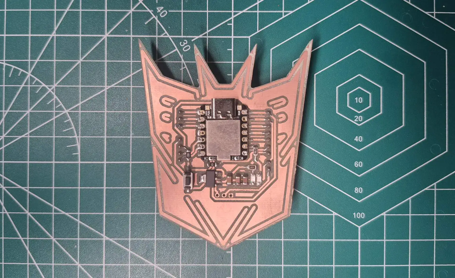
Final Result
After completely soldering the PCB, I uploaded a very simple test code, when the button is pressed, the LED turns on.
const int pinButton = D3;
const int pinLed = D8;

void setup() {
  pinMode(pinLed, OUTPUT);

  pinMode(pinButton, INPUT);
}

void loop() {
  int ButtonState = digitalRead(pinButton);

  if (ButtonState == HIGH) {
    digitalWrite(pinLed, HIGH);
  } else {
    digitalWrite(pinLed, LOW);
  }
}