Electronics Design
For this week's group assignment, we familiarized ourselves with the essential lab equipment for observing the operation of a microcontroller. We worked hands-on with a multimeter, an oscilloscope, and a logic analyzer.
Group Assignment Week 6
During this session, I discovered new advanced oscilloscope options for analyzing signals more accurately. Furthermore, I finally understood the internal logic behind the operation of the multimeter and the signal analyzer for measuring electrical properties and decoding digital logic
This week, I explored the entire electronics design process. I designed a custom multi-purpose board using a Xiaomi ESP32-C3, simulated a circuit, and compared different EDA tools, Altium and KiCad. Finally, I used CAD software to design a custom enclosure for the final circuit.
Simulation of a Zener Trimmer Circuit
The idea to simulate a Zener diode clipping circuit arose from a practical requirement for my board. I needed a way to safely reduce the 7.4V input voltage from the external battery powering the XIAO ESP32-C3. Although I ultimately didn't implement this Zener configuration in the final PCB design, opting instead for an AMS1117 linear regulator, simulating it in Altium Designer was valuable practice.
Getting Started with Altium Designer
Schematic of the Voltage Regulator with Zener Diode
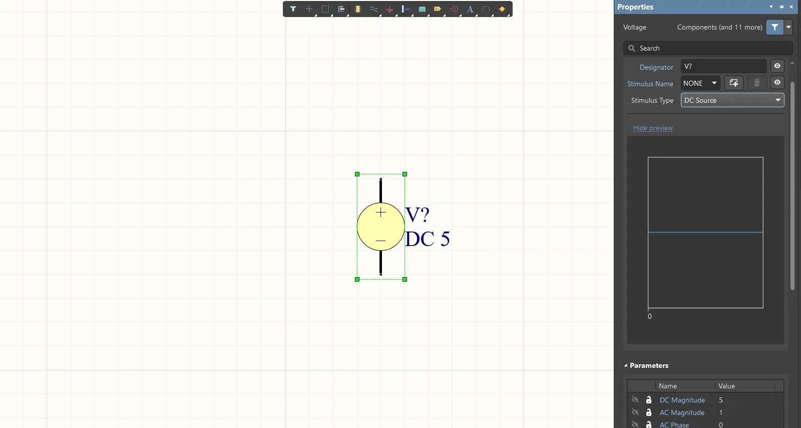
With all the components placed, I connected them using the Wiring tool. This step is crucial to ensure that the simulator understands how the components interact with each other. After wiring, I was ready to configure the simulation parameters.
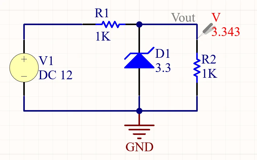
The virtual probe displays a voltage set to 3.343 V. Unlike conventional diodes, a Zener diode is designed to operate safely in reverse. When a 12 V input reaches the diode, it enters avalanche breakdown at its 3.3 V threshold, preventing any higher voltage from passing.
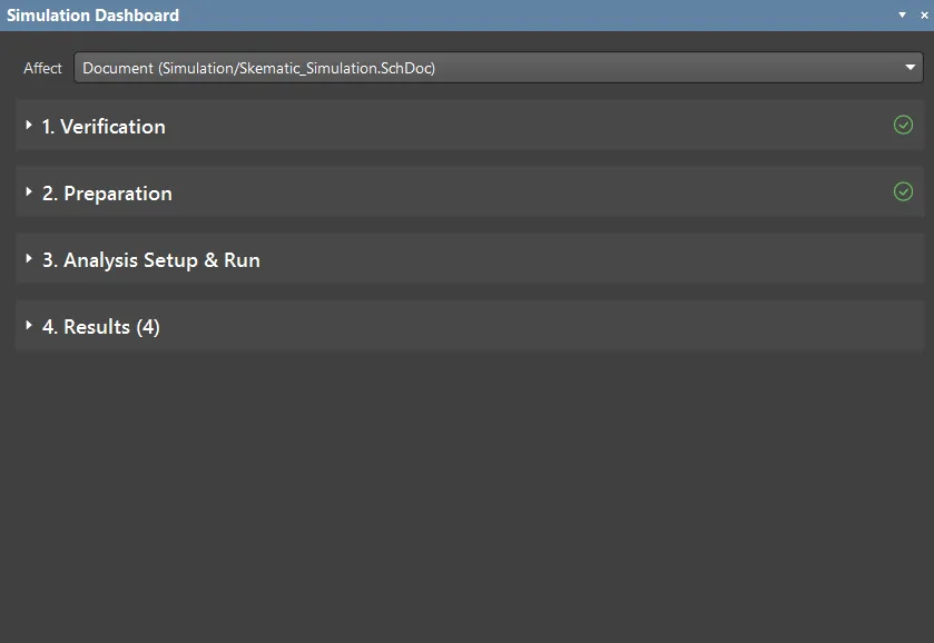
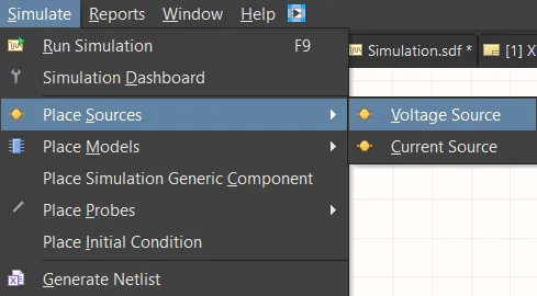
Simulation Dashboard
This panel is a step-by-step control center for testing circuits. It organizes the workflow into three simple steps.
- Verification: The drawing is reviewed for errors and to ensure it can be simulated.
- Preparation: The power supplies, such as the 12V input and test probes, are configured.
- Analysis Setup: The specific test is configured, and the individual simulation is run.
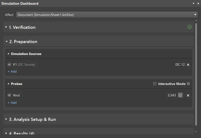
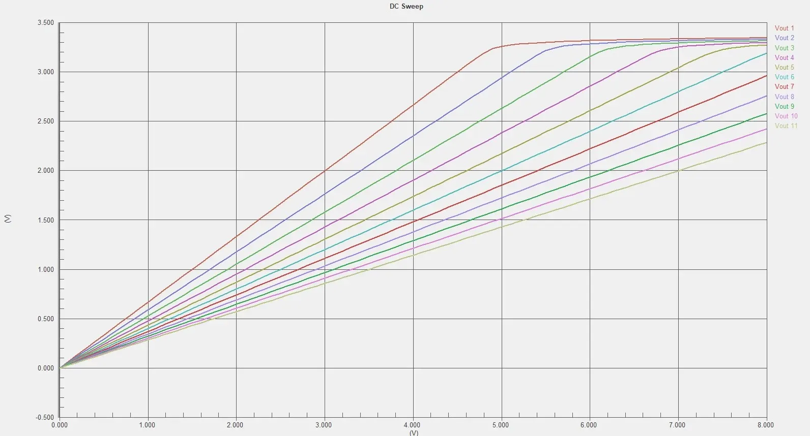
On the Preparation tab, I confirmed that the primary 12 V DC source, V1, was active and enabled a Vout voltage probe to monitor the output node. Next, in the Analysis Settings, I configured a DC sweep. I set the primary voltage source sweep from 0 V to 8 V and added a secondary parametric sweep for resistor R1, varying it from 500 Ω to 2.5 kΩ. This combined configuration allows the simulator to calculate how the Zener diode reacts to variations in input voltage and different load conditions simultaneously.
Graphical Result of the Simulation
The resulting DC sweep graph perfectly visualizes the clamping behavior of the Zener diode. The X-axis represents the input voltage sweep from 0 V to 8 V, while the Y-axis shows the resulting output voltage. The multi-colored lines Vout 1 to 11 represent the secondary parametric sweep of resistor R1, which varies from 500 Ω to 2.5 kΩ. As the input voltage increases, output voltage increases proportionally. Crucially, once the output approaches 3.3 V, all the curves flatten out completely, reaching a plateau. This clearly demonstrates that the Zener diode successfully enters avalanche breakdown, safely limiting the voltage regardless of the input or specific load.
PCB Design in Altium Designer
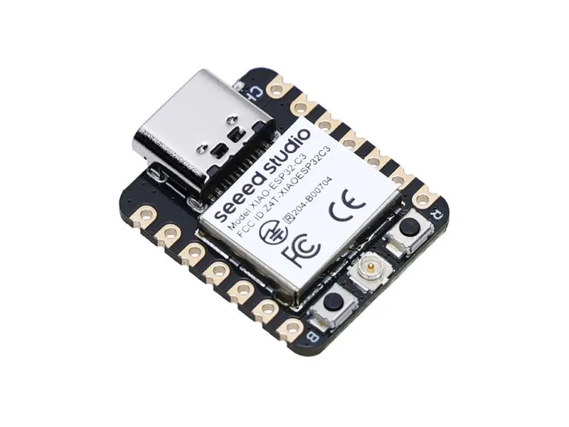
As I mentioned before, I decided to design my custom board around the Seeed Studio XIAO-ESP32-C3. I specifically chose this microcontroller because it's exactly the board I planned for my final project. Familiarizing myself with its footprint, pin layout, and routing requirements now will give me a significant advantage.
-
Processor: 32-bit RISC-V single-core up to 160 MHz.
A powerful core capable of handling complex logic, sensor reading, and communication tasks efficiently for the final project. -
Wireless Connectivity: Built-in 2.4GHz Wi-Fi and Bluetooth 5.
Provides complete wireless capabilities, and it includes a U.FL connector to attach an external antenna to significantly boost the RF range. -
Rich Interfaces: 11 digital I/O (PWM), 4 analog (A0-A3), I2C, SPI, and UART.
Despite its tiny thumb-sized form factor, it offers massive flexibility for connecting multiple sensors and communication protocols.
Pinout XIAO-ESP32-C3
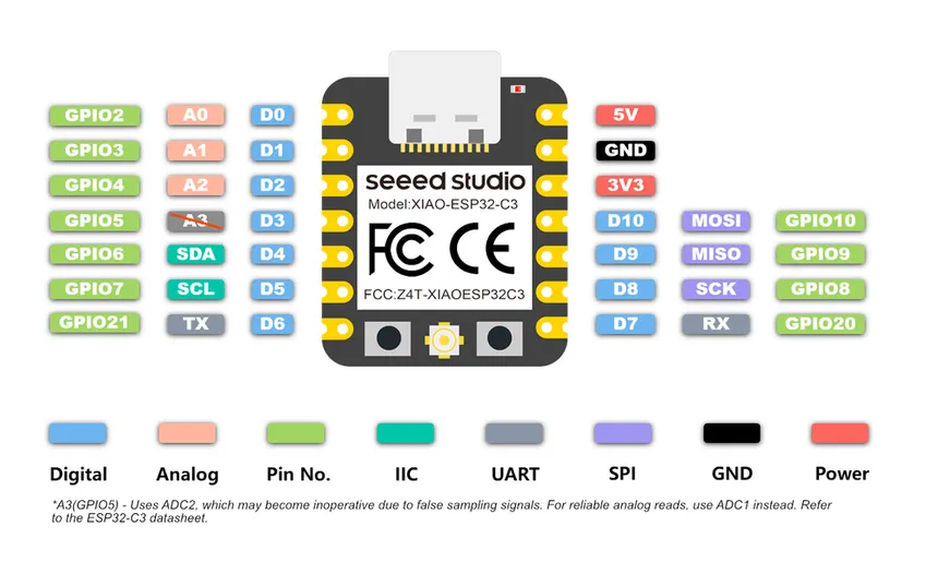
Note:
Pin A3 (GPIO5) loses its analog reading capabilities when Wi-Fi is active because they share the same internal resource (ADC2). To avoid hardware conflicts, all analog sensors must be routed to pins A0, A1, or A2 instead.
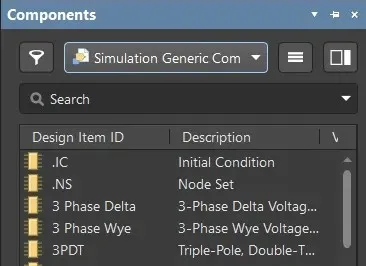
The first phase involves collecting all the necessary schematic symbols and physical footprints for the components.
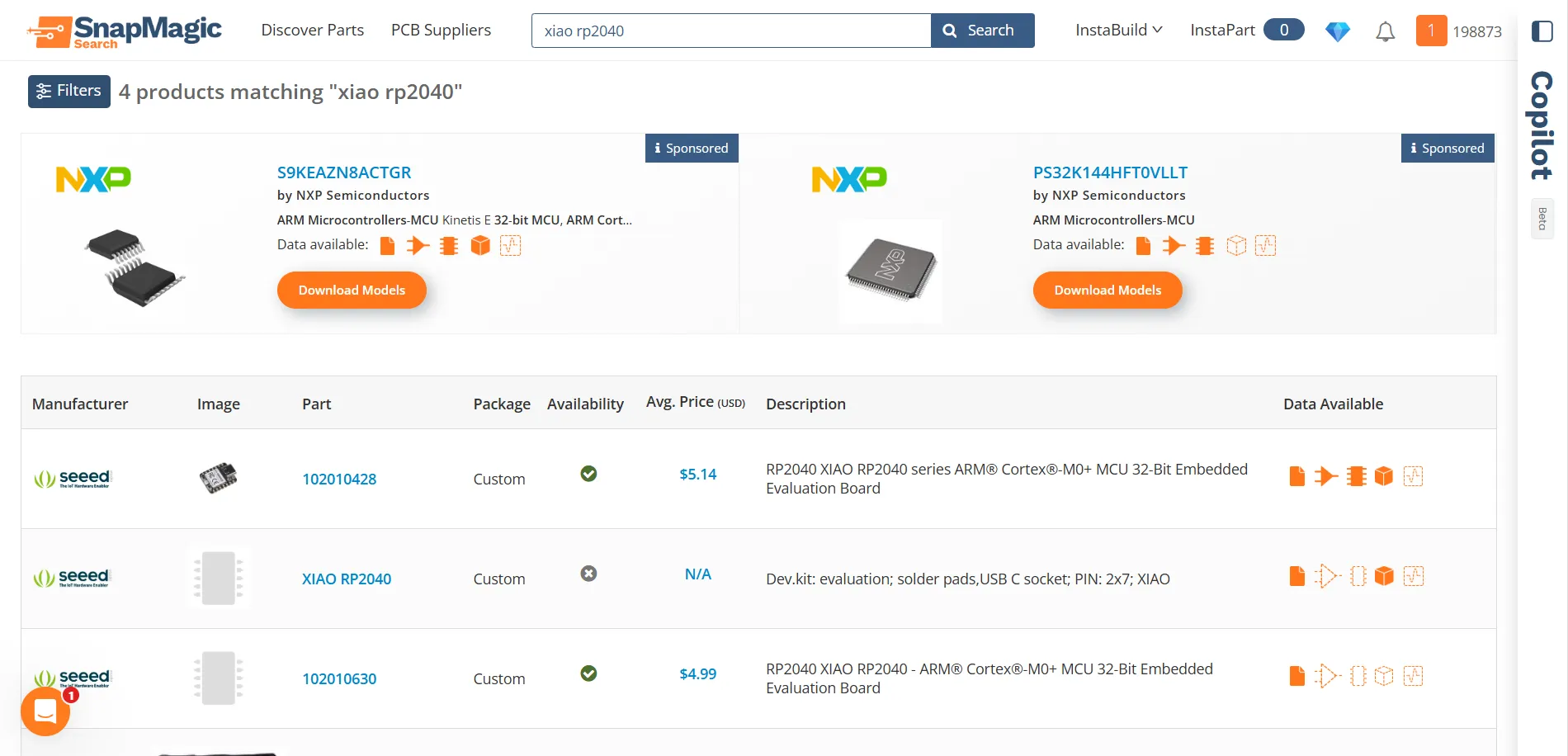
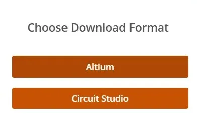
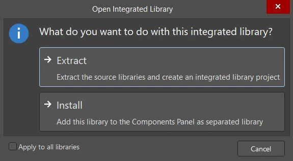
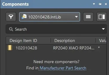
Since I couldn't find the XIAO microcontroller in the default Altium libraries, I decided to search for it on SnapMagic Search.
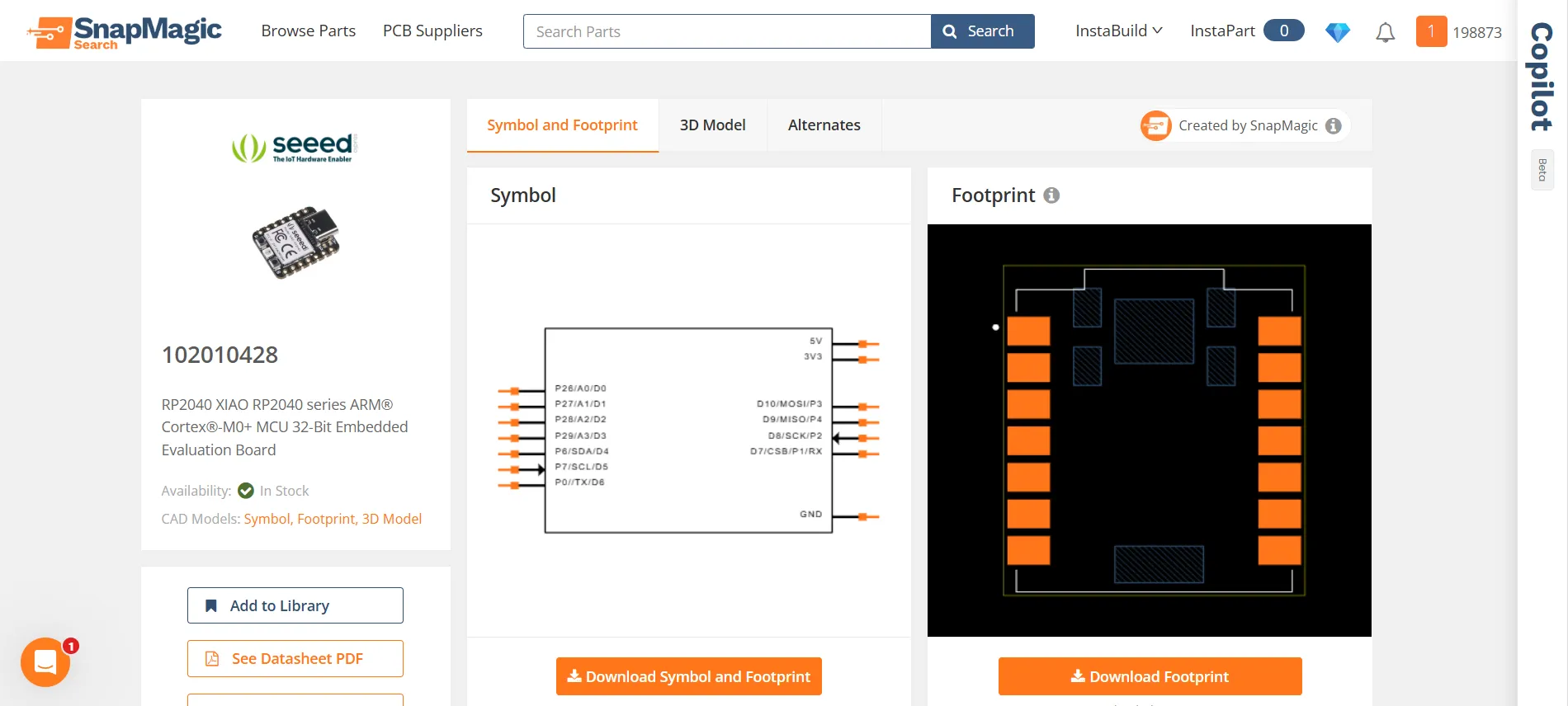
While custom components, such as the microcontroller, were sourced externally, the rest of the schematic was created using Altium's native tools and built-in databases. This ensures a streamlined process and that standard components include footprints and 3D models.
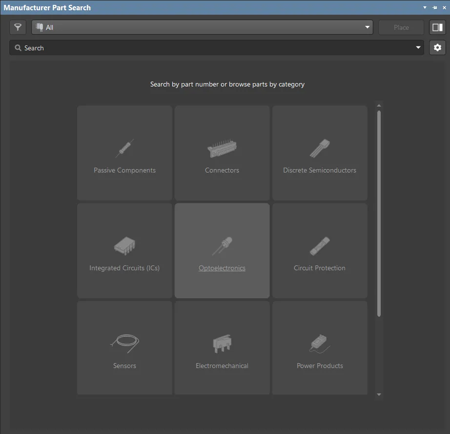
Manufacturer Part Search
For standard passive components like resistors, capacitors, LEDs, and regulators, as well as the pin headers for the inputs and outputs, I used the integrated Manufacturer Part Search panel. This tool is incredibly useful because it fetches parts directly from suppliers, complete with verified schematic symbols and physical footprints.
Drafting the Schematic Essential Tools
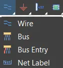
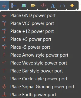
The following tools are essential for connecting the circuit schematic.
- Wire: The primary tool used to draw physical electrical connections between component pins.
- Net Label: Used to logically connect distant pins across the schematic by giving them the same name. This keeps the drawing clean and prevents a mess of intersecting lines.
- GND Power Port: The standard ground symbol, essential for establishing the 0V reference point to complete the circuit loop.
- VCC / +5V / +3.3V Ports: Used to distribute power from the regulators to the various components without drawing long, cluttered wires all over the page.
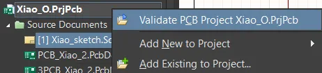
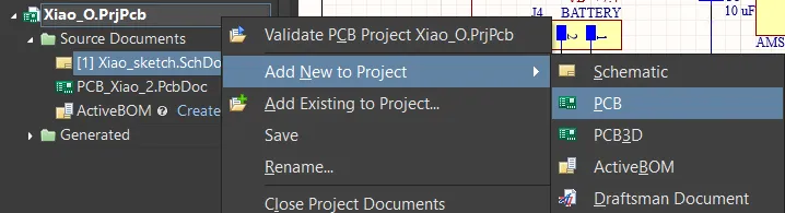
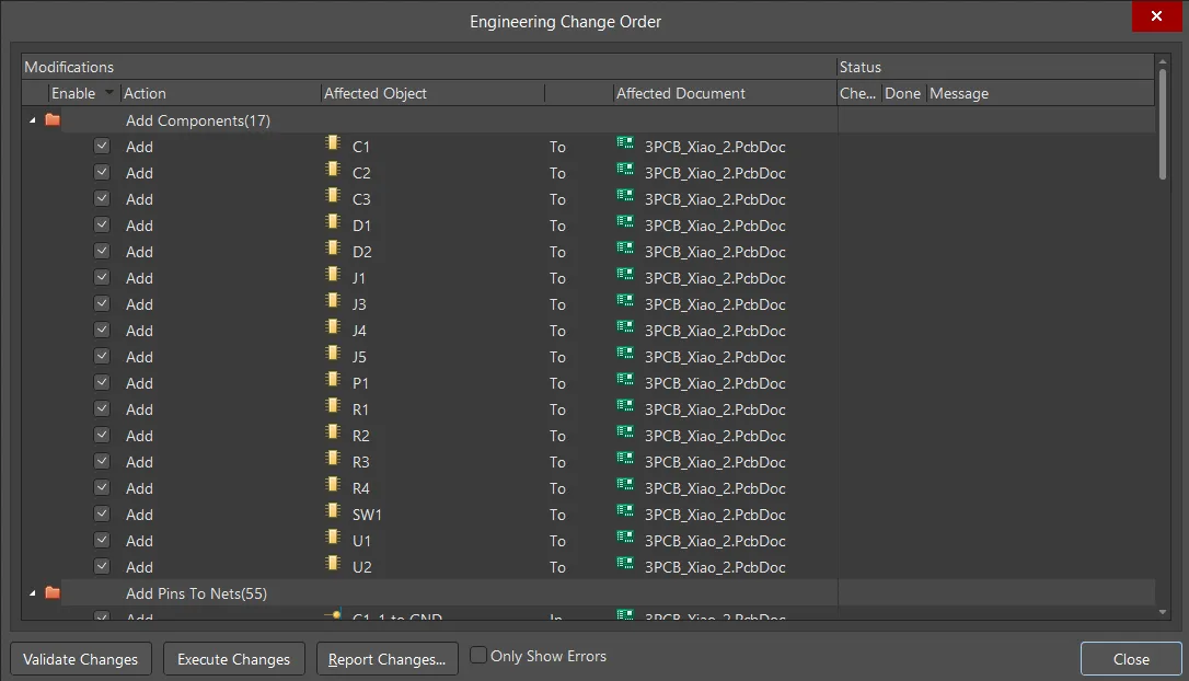
Validate PCB Project
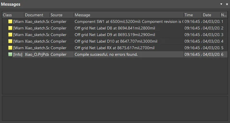
Before moving to the PCB layout, the next step is to validate the schematic design. By compiling the project, Altium evaluates the logical connections and overall integrity of the circuit.
The generated message report showed a successful compilation with zero errors, but it flagged 5 minor warnings, which I ignore for this design
These warnings indicate that some net labels and a switch component were placed slightly off the standard drawing grid. Because these are purely visual alignment warnings within the schematic editor, they do not affect the electrical connectivity or the functionality of the circuit in any way.
Since the compiler confirmed Compile successful, no errors found, the schematic is fully verified and ready to be transferred to the physical PCB environment.
Schematic of the Custom Board
With all the necessary traces and symbols gathered, I assembled the final schematic of my custom board. To maintain a clean design, I organized the circuit into functional blocks using network labels instead of drawing long, intersecting wires. This modular approach makes the board's architecture very easy to understand at a glance.
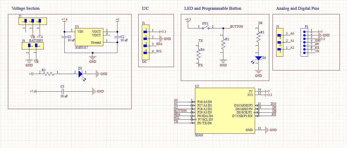
- Microcontroller: The Seeed Studio XIAO (RP2040) acting as the brain of the board.
- Power Management:Battery input pins, a main power switch and a 5V AMS1117 voltage regulator to safely distribute power and place an LED that indicates if 5V is coming out of the regulator.
- User Interface: A programmable button and a programmable LED.
- Expansion Headers: Dedicated breakout pins for Digital I/O, Analog inputs, and a specific I2C communication port for future sensors.
- Passive Components: Supporting hardware including decoupling capacitors, current-limiting resistors, and a 0-ohm resistor for routing flexibility.
Designing PCBs in Altium
With the circuit schematic completed, I moved on to the physical PCB design.
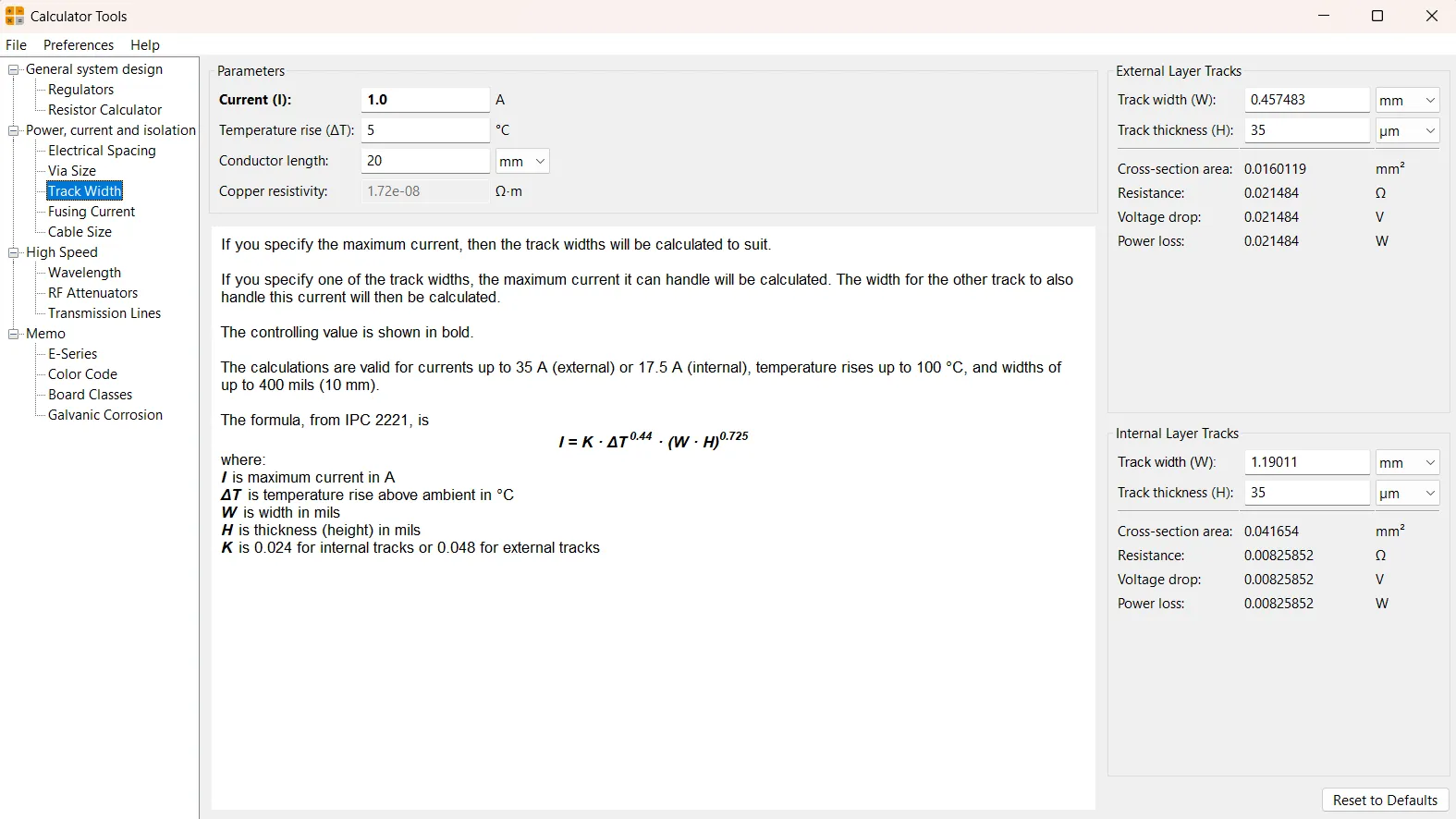
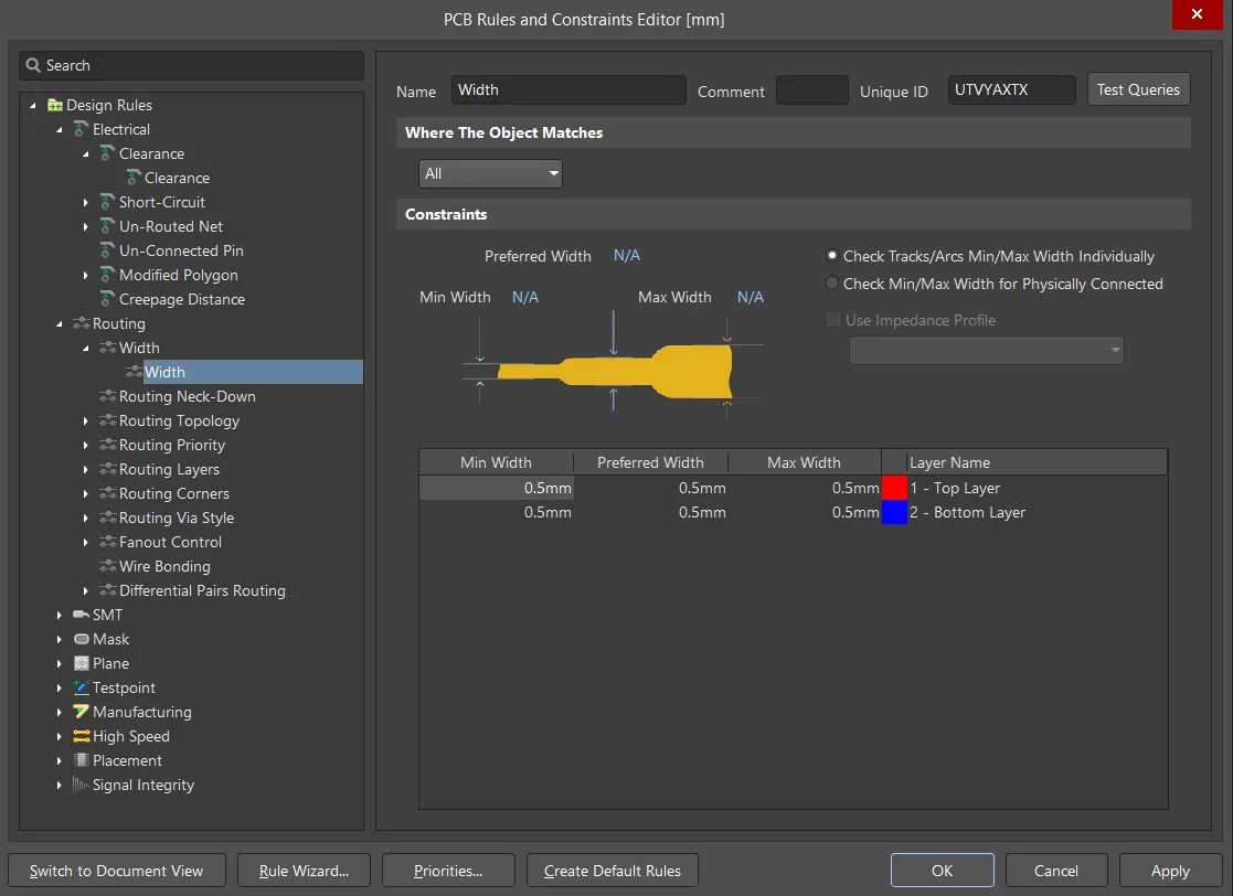
First, I used KiCad's internal Calculator Tools. Calculating for a 1 A current and a 5 °C temperature rise resulted in a 0.45 mm width. For practical fabrication purposes and to guarantee the milling bit can carve the traces without issues, I rounded the final design rule up to 0.5 mm.
Then I started the PCB design process.
After determining the design rules, I can begin arranging and connecting the components on my PCB.
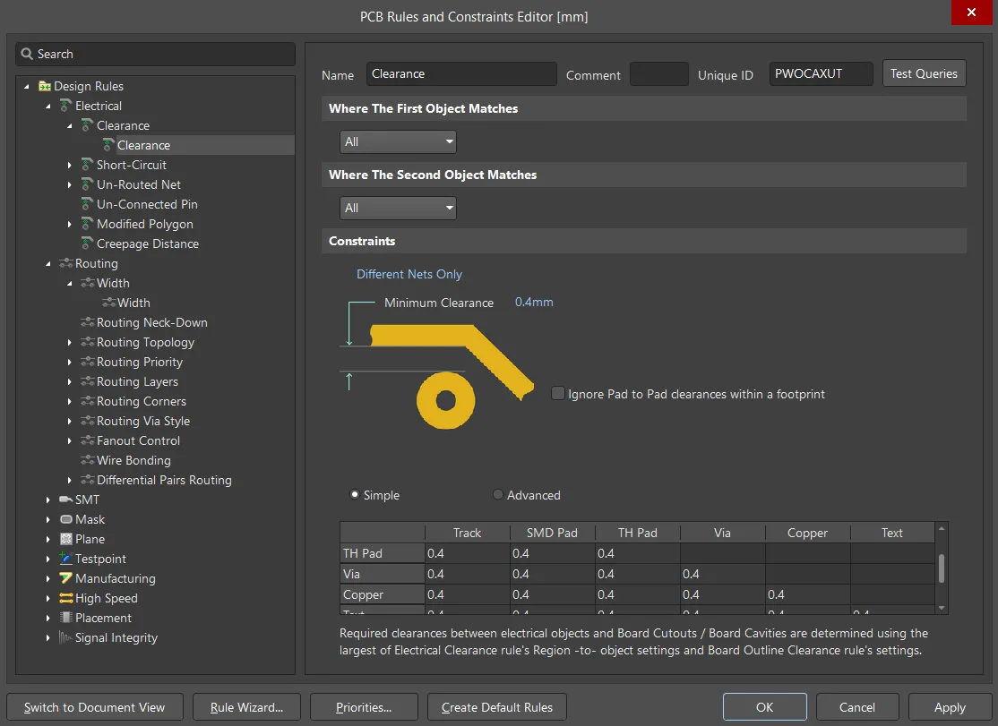
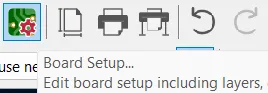
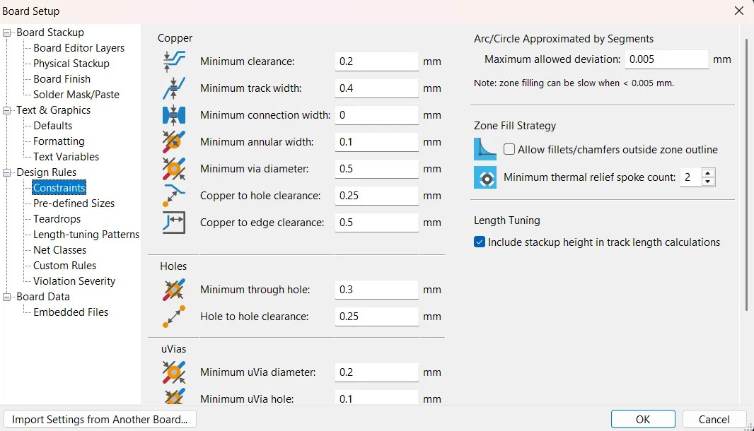
Design Rules Check
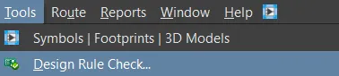
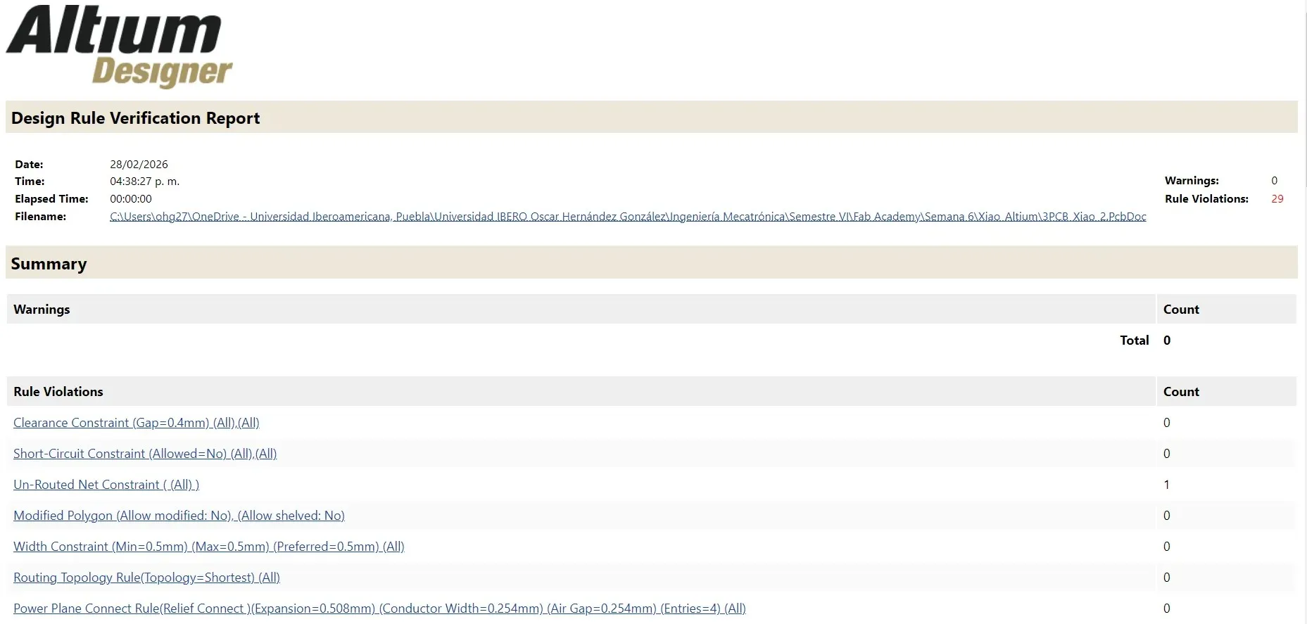
After fully routing the PCB, the next step is to run a Design Rules Check. By going to Tools > Design Rules Check..., Altium evaluates the board according to the previously defined constraints.
The generated verification report flagged 29 rule violations, which I deemed safe to ignore for this specific manufacturing process:
1 Unrouted network restriction. This single unrouted connection is intentional. It corresponds to the 0 ohm resistor I'm using as a jumper. Although the software marks it as a broken trace, the physical component will complete the circuit once soldered.
Silkscreen and annotation violations. The remaining warnings are simply indicators of components overlaid with copper pads or traces. Since this board will not be manufactured at this time, these visual text overlays do not affect the physical fabrication or functionality of the board in any way.
Custom PCB Shape in Altium
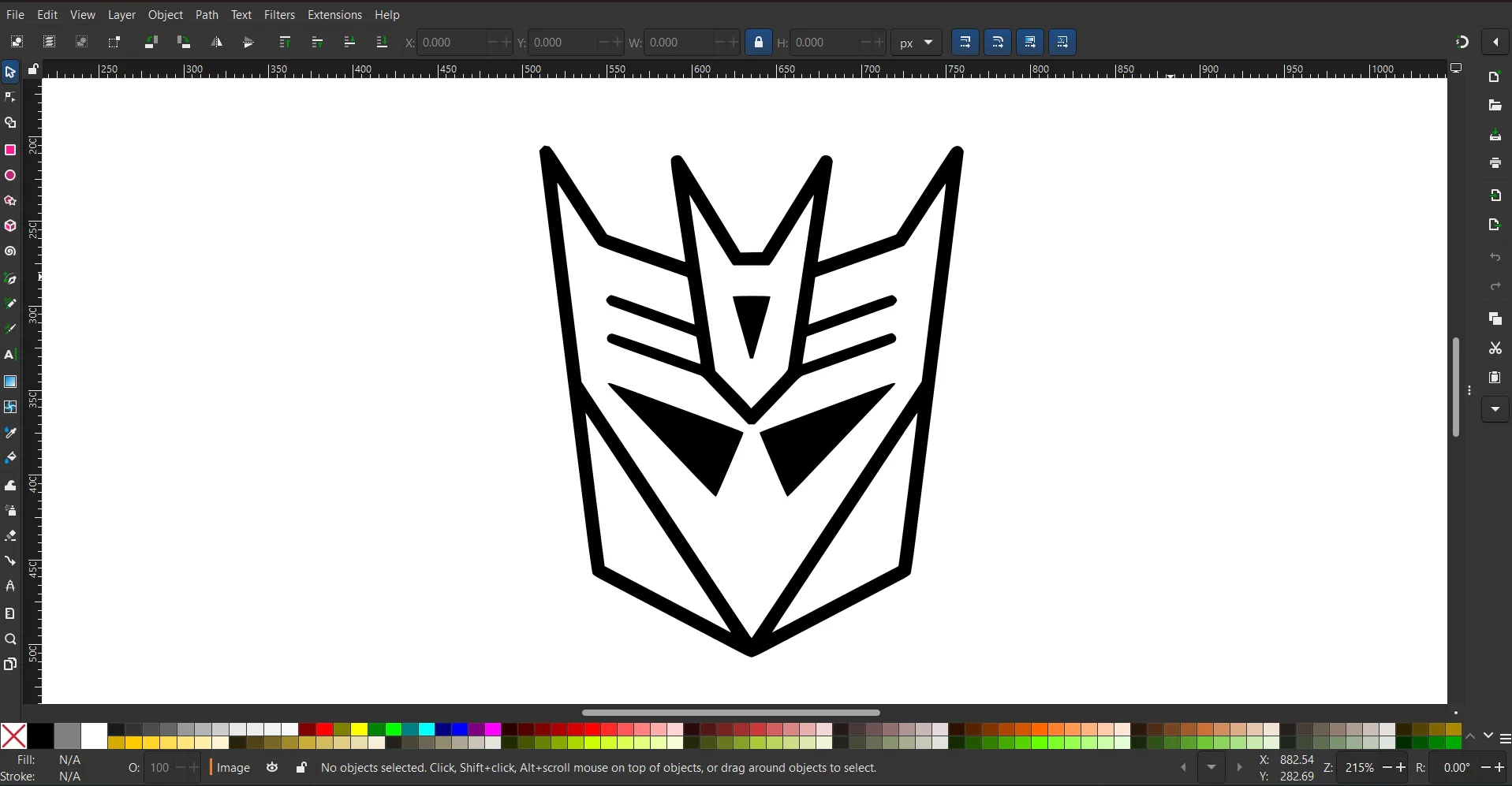
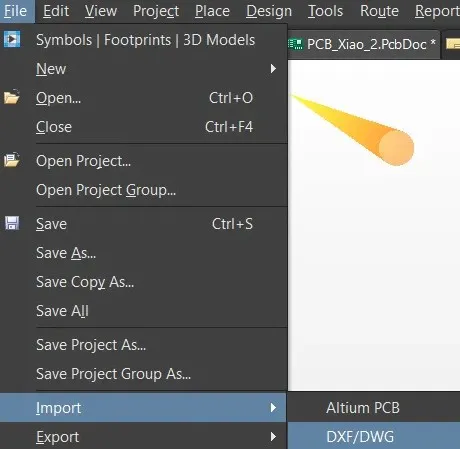
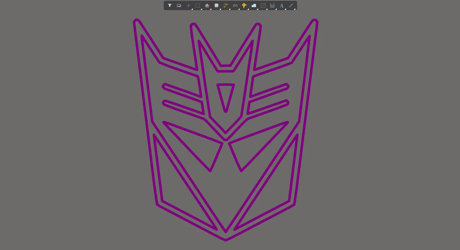
To give the board its unique character, I decided to shape it after the Decepticons logo. Since the software isn't designed for complex 2D graphic designs, I started this process outside of Altium. I used Inkscape to trace and vectorize a reference image of the logo. Once I had a clean, continuous vector outline, I exported it as a .DXF file, the standard CAD format for transferring 2D geometry.
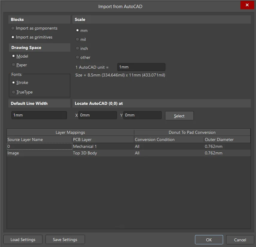
Within Altium's .PcbDoc file, I went to File > Import > DXF/DWG to import the custom vector from Inkscape into my workspace. During the import setup, I made two crucial adjustments: I set the scale to mm to match my project's units and assigned the source vector to the Mechanics 1 layer. This assignment is essential, as it tells Altium that these imported lines represent the physical boundaries of the board, rather than electrical copper traces.
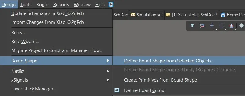
After successfully importing the purple vector logo into the Altium environment, I carefully selected its outer continuous line. With this main perimeter highlighted, I used the command Design > Board Shape > Define Board Shape from Selected Objects. This action instantly cropped the standard black canvas of the workspace to perfectly match the custom outline of the Decepticon.
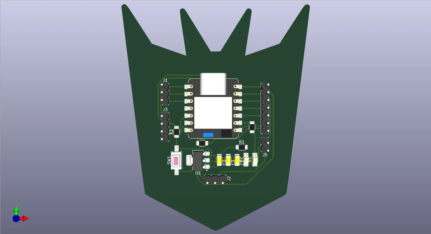
Final Result in Altium Design
Micro-Con-C3 Altium Files
PCB Design in KiCad
To compare the design process and user experience, I also recreated the same schematic and PCB design in KiCad. The workflow is very similar, but the interface and specific tools differ.
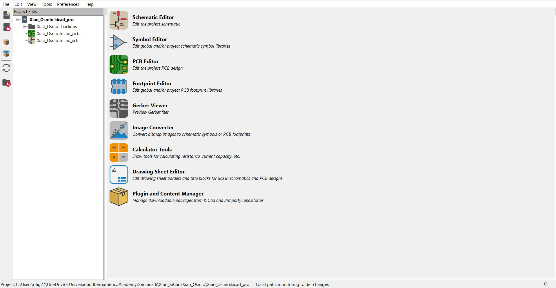
Getting Started with KiCad
Working in KiCad begins in the main project panel, which centralizes all the necessary tools, such as the schematic and PCB editors. However, before drawing any circuits, I needed to ensure I had the correct component models with footprints and schematics.
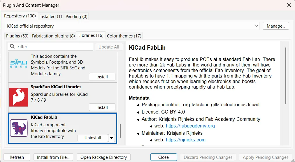
Instead of searching for standard components on external websites, I opened the Plugin and Content Manager directly from the main menu. From the "Libraries" tab, I searched for and installed KiCad FabLib. This essential library contains verified symbols, footprints, and 3D models.
With FabLib installed correctly, I opened the Schematic Editor to begin drawing the circuit. Design in KiCad relies heavily on the vertical toolbar located on the right side of the screen.

Essential Tools for Schematic Drafting
- Add a symbol the Triangle/Op-Amp icon: This is the primary tool for opening the library browser and placing standard components such as resistors and capacitors, as well as FabLib's custom XIAO-ESP32-C3.
- Add a power port the Ground icon: Essential for quickly inserting power reference symbols like GND, +5V, and +3.3V without cluttering the page.
- Add a wire the blue diagonal line: The fundamental tool for drawing the physical electrical connections between component pins.
- Add a network label the "A" icon: Similar to Atium Design, this tool is crucial for logical connections. By assigning the same name to different pins, KiCad virtually links them, preventing a tangle of crossed wires.
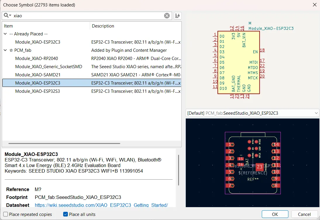
Component Selection
Clicking the Add a Symbol tool opens the component selector window. This interface provides a preview of both the schematic symbol and the physical PCB footprint of any selected component. I made sure to source all the components for my circuit, from the XIAO microcontroller to the passive resistors and LEDs, exclusively from the installed KiCad FabLib.
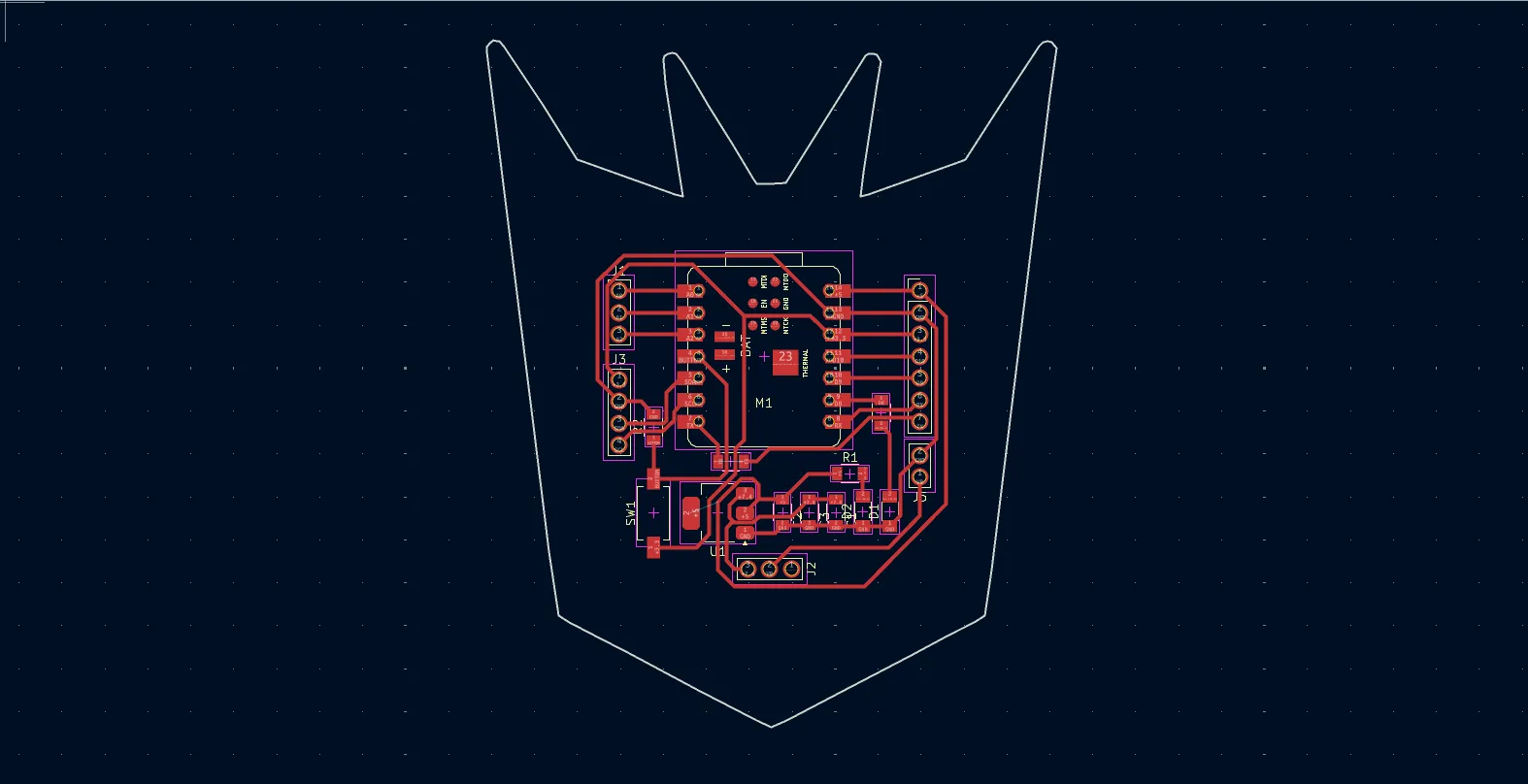
Schematic of the Custom Board
Using the tools described above, I recreated the complete schematic of the custom board. As with my previous design, I used network labels to organize the circuit into logic blocks, maintaining a clean and legible layout.
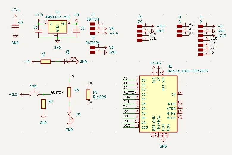
One important detail to note in this version of KiCad is the symbol for the XIAO microcontroller. Unlike the model I found for Altium, which only included the standard external crenellated pins, this official FabLib model includes all the additional surface-mount pads located on the underside of the physical XIAO board, such as the battery connections and test pins. This comprehensive representation provides a much more accurate depiction of the actual hardware and offers greater flexibility for routing.
Designing PCBs in KiCad
With the circuit schematic completed, I moved on to the physical PCB design.
With the setup complete, I began the final step of the PCB design
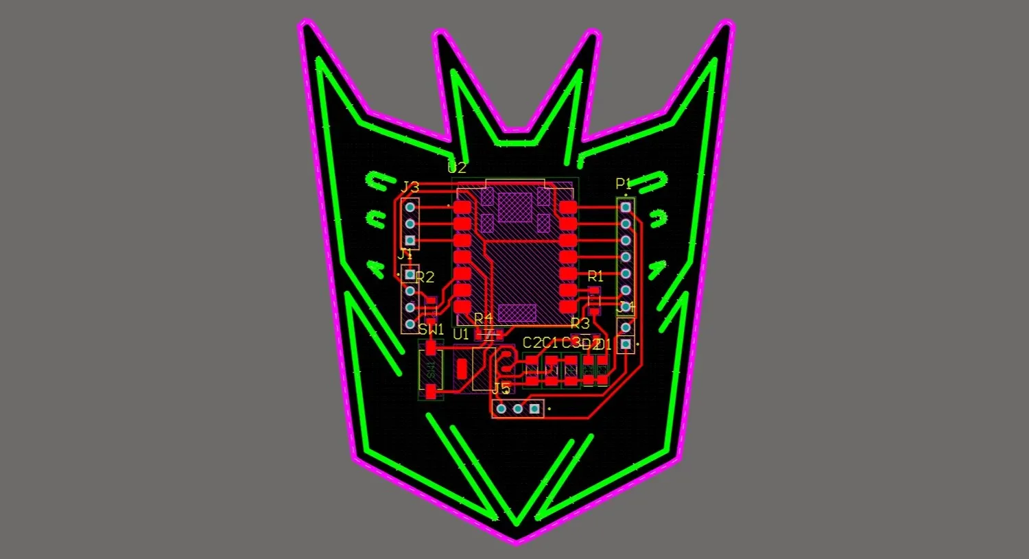
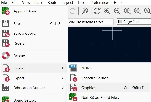
Custom Board Shape in KiCad
Just like in my previous workflow, I wanted to give my KiCad board the custom Decepticon shape.
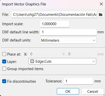
I navigated to File > Import > Graphics... to bring in my .DXF file. In the import setup dialog, I ensured the units were set to Millimeters to match my design scale, and most importantly, I set the target layer to Edge.Cuts. In KiCad, the Edge.Cuts layer is specifically dedicated to defining the physical outer boundary of the PCB. Once imported, the vector outline perfectly framed my workspace, instantly creating the custom board shape without needing any additional cropping commands.
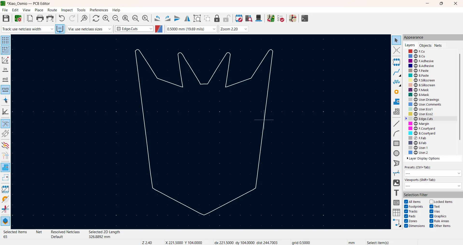
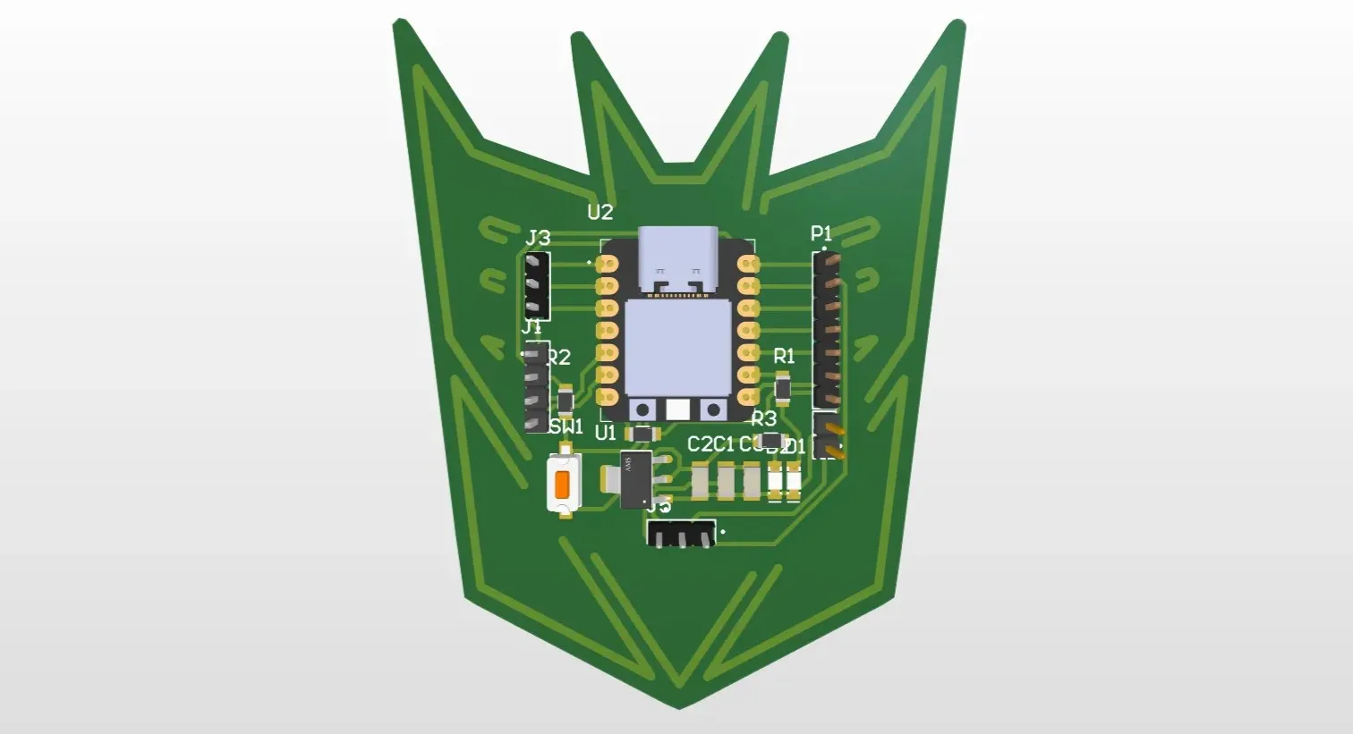
Final Result in KiCad
Micro-Con-C3 KiCad Files
Altium Designer vs. KiCad
After delving into both Altium Designer and KiCad, I was able to experience their respective advantages and disadvantages firsthand. Altium excels by offering a wide variety of parts readily available in its integrated library, whereas KiCad requires the manual installation of specific libraries; without them, it can be quite difficult to find parts with linked footprints and schematics. However, I found KiCad's interface to be a bit more intuitive. It is worth mentioning that Altium includes more advanced tools that help produce highly professional work, although both software programs are incredibly comprehensive. Ultimately, KiCad's main advantage is that it is free, open-source software, which is not the case with Altium.
Personally, I will continue using Altium Designer for my projects. I am already familiar with the software's workflow and have successfully designed and manufactured physical PCBs with it in the past