

Week 08
Electronics Production
Check out our Group Assignment to see the characterization of the design rules for our in-house PCB production process: GROUP PAGE →
// WHAT IS A PCB? \\
A Printed Circuit Board (PCB) is the foundational building block of most modern electronic devices. It mechanically supports and electrically connects electronic components using conductive tracks, pads, and other features etched from copper sheets laminated onto a non-conductive substrate. In today's technology, PCBs are crucial because they allow for the miniaturization, reliability, and mass production of complex circuits.
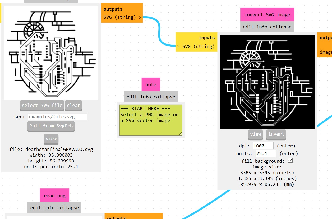
For this week, I will be utilizing a DIY in-house manufacturing process. This involves exporting a vectorized PNG or SVG file to mill the traces onto conductive copper plates using a Roland Monofab. Once the board is milled, the final step is to manually solder all the necessary SMD (Surface-Mount Device) components.
Defining the Design
I am a huge Star Wars fan, and for this assignment, I was incredibly inspired by the design of the Death Star. To me, it looks like a giant, intergalactic lunar microchip. I wanted to capture that essence in my PCB layout.

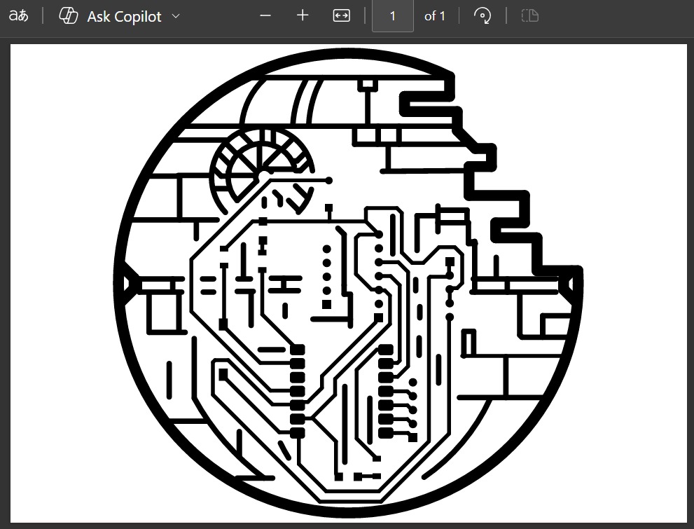
The reference image that inspired my deathstar based PCB.
A couple of weeks ago, I used Altium Designer to sketch out some initial concepts. However, for this week, I made the decision to design a very complete prototype board that I will actually use to build my final proyect.
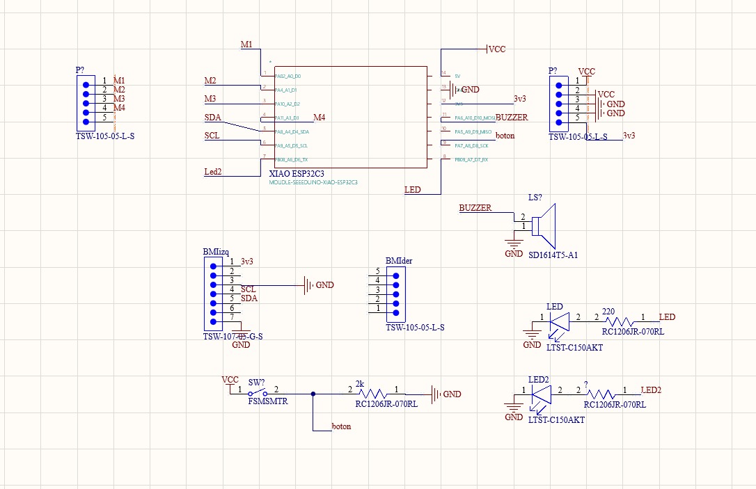
The schematic for the PCB.
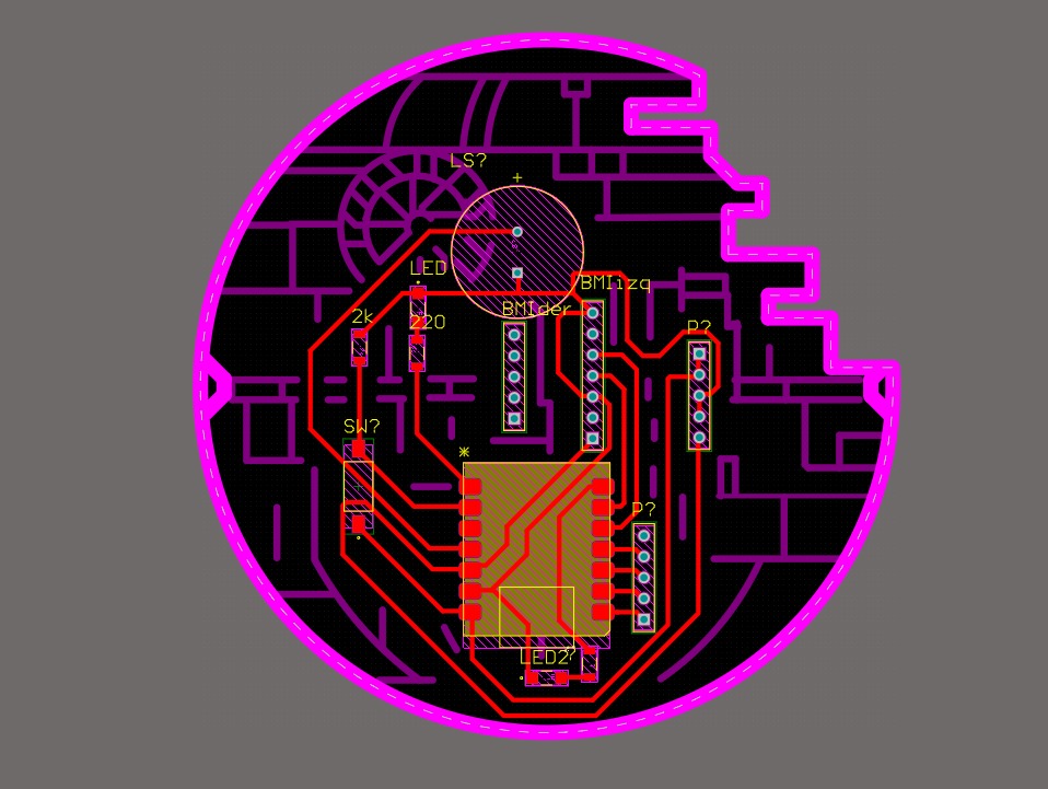
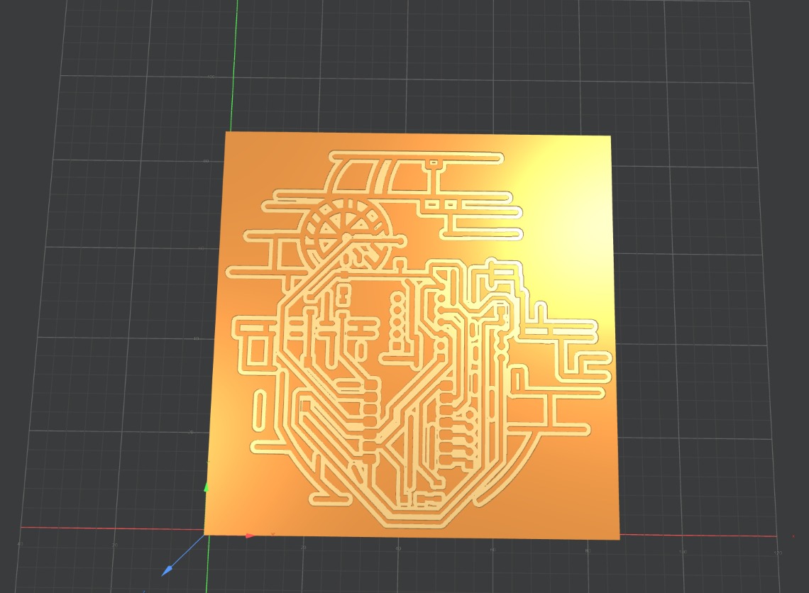
The 3D virtual PCB layout featuring the Death Star aesthetic.
To ensure the design not only looked beautiful but milled perfectly, I intentionally made the dark purple traces (the engraving lines) thicker. This guarantees that the Roland Monofab will clearly identify and isolate the design during the cutting process.
Inkscape Workflow
Exporting the PDF
As I documented in the Electronics Design week, the first step is to generate a clean PDF containing only the necessary layers (traces and board outline).
The exported PDF from Altium showing the raw trace layout.
Scaling and Vectorizing in Inkscape
Once the PDF is generated, we move to Inkscape to create the SVG files required by the CAM software. A crucial step here is verifying the scale, as dimensions can sometimes shift during the PDF import.
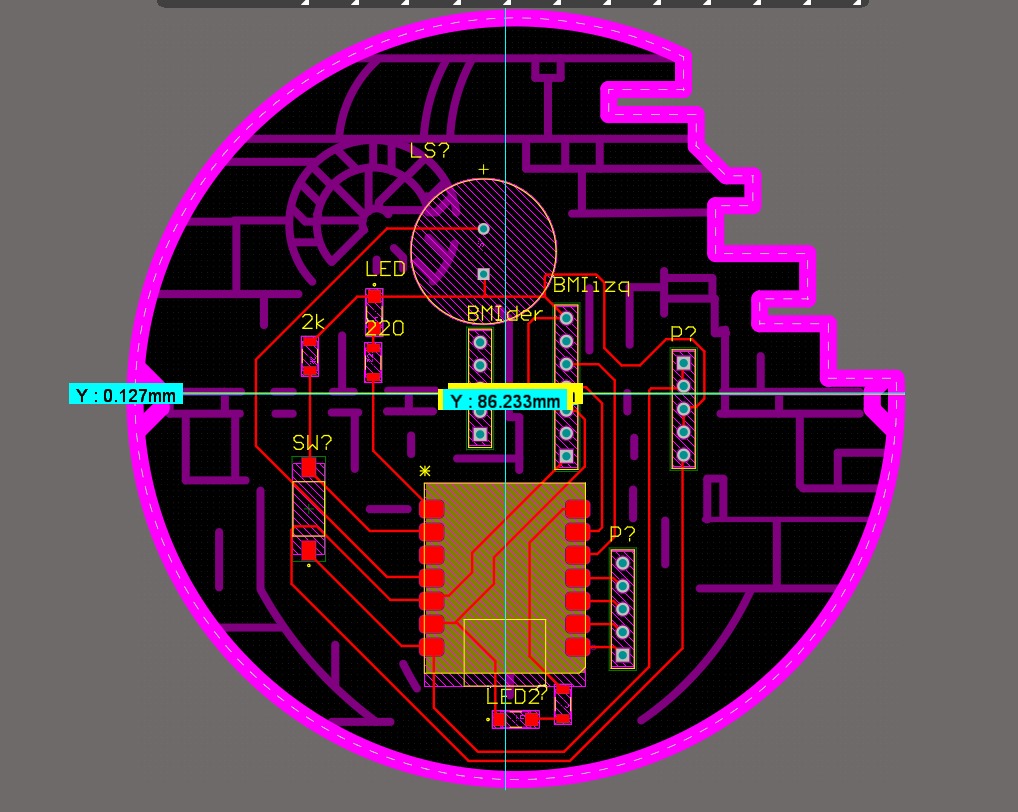
Measuring the exact board dimensions in Altium using Ctrl + M.
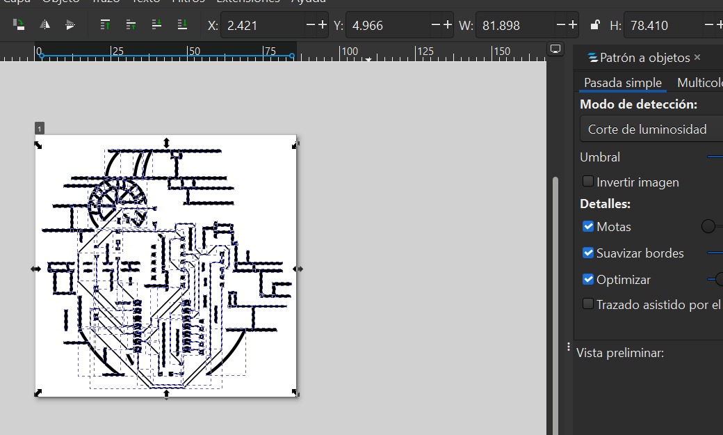
Adjusting the document properties and object size in Inkscape to match the exact Altium dimensions.
After the scale is perfectly matched, the next step is to vectorize the bitmap (if necessary) and separate the design into two distinct SVG files:
1. Traces (Engraving): The paths the V-bit will follow to isolate the copper circuits.
2. Outline (Cutting): The exterior border where the endmill will cut completely through the board to release the PCB.
CAM Preparation with Mods Project
To generate the RML files for the Roland, we use a web-based tool heavily utilized in Fab Academy called Mods Project (or Mods CE).
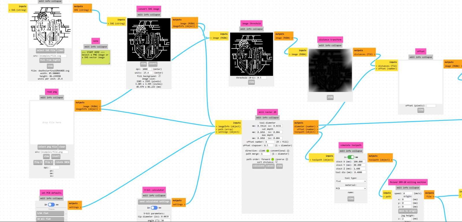
The modular, node-based interface of Mods Project. It's quite intuitive but requires close attention to detail to avoid ruining the cut.
1. Traces Setup (Engraving)
For the traces, we must import the first SVG. A vital step here is to invert the image so the machine understands it needs to mill around the white traces, removing the black areas.
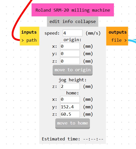
Next, we must correctly define our origins (X:0, Y:0, Z:0) in the Roland SRM-20 node.
Offsets are critical: In the calculation node, the "offset" parameter dictates how many passes the tool will make around the trace. We need multiple passes to ensure no copper bridges are left behind, which could accidentally short-circuit the board.
2. Outline Setup (Cutting)
For the exterior cut, the process is much simpler. We import the outline SVG, select the "Mill Outline" default configuration, and generate the path.
3D Simulation
Mods Project features a very helpful 3D simulation viewer where you can inspect the final result of both toolpaths on a virtual board.
3D simulation of the engraved traces.
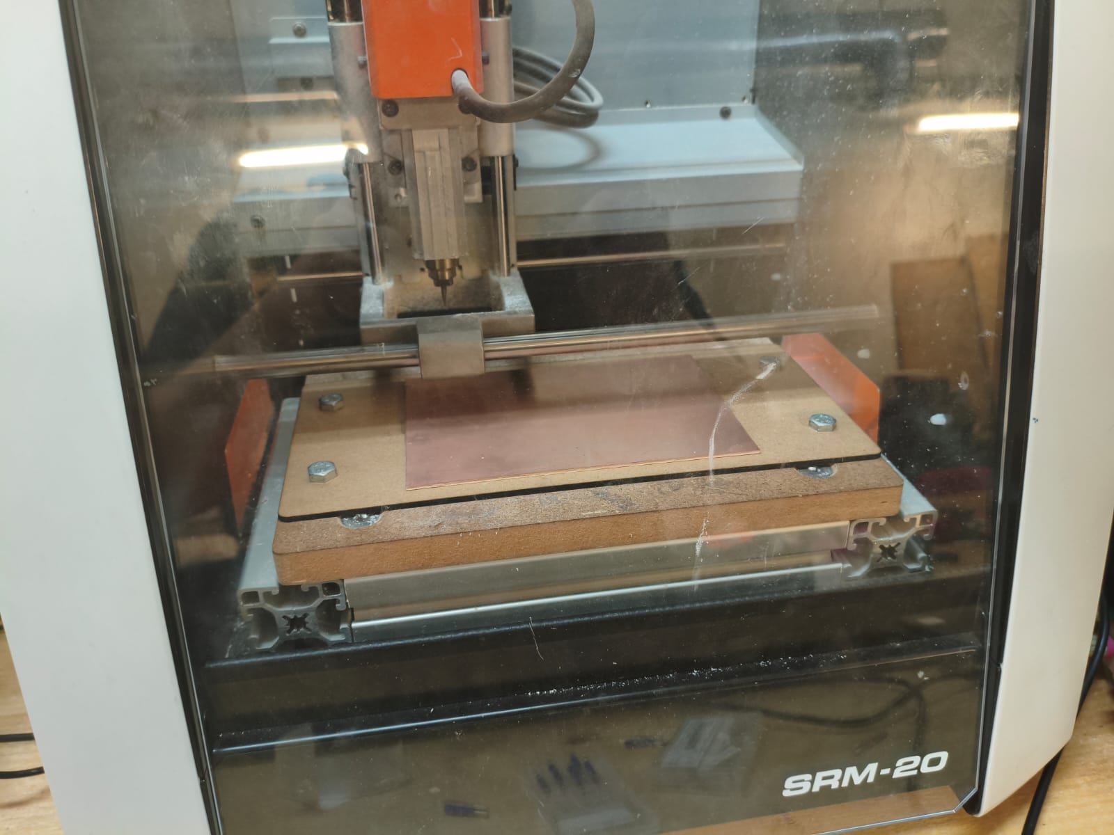
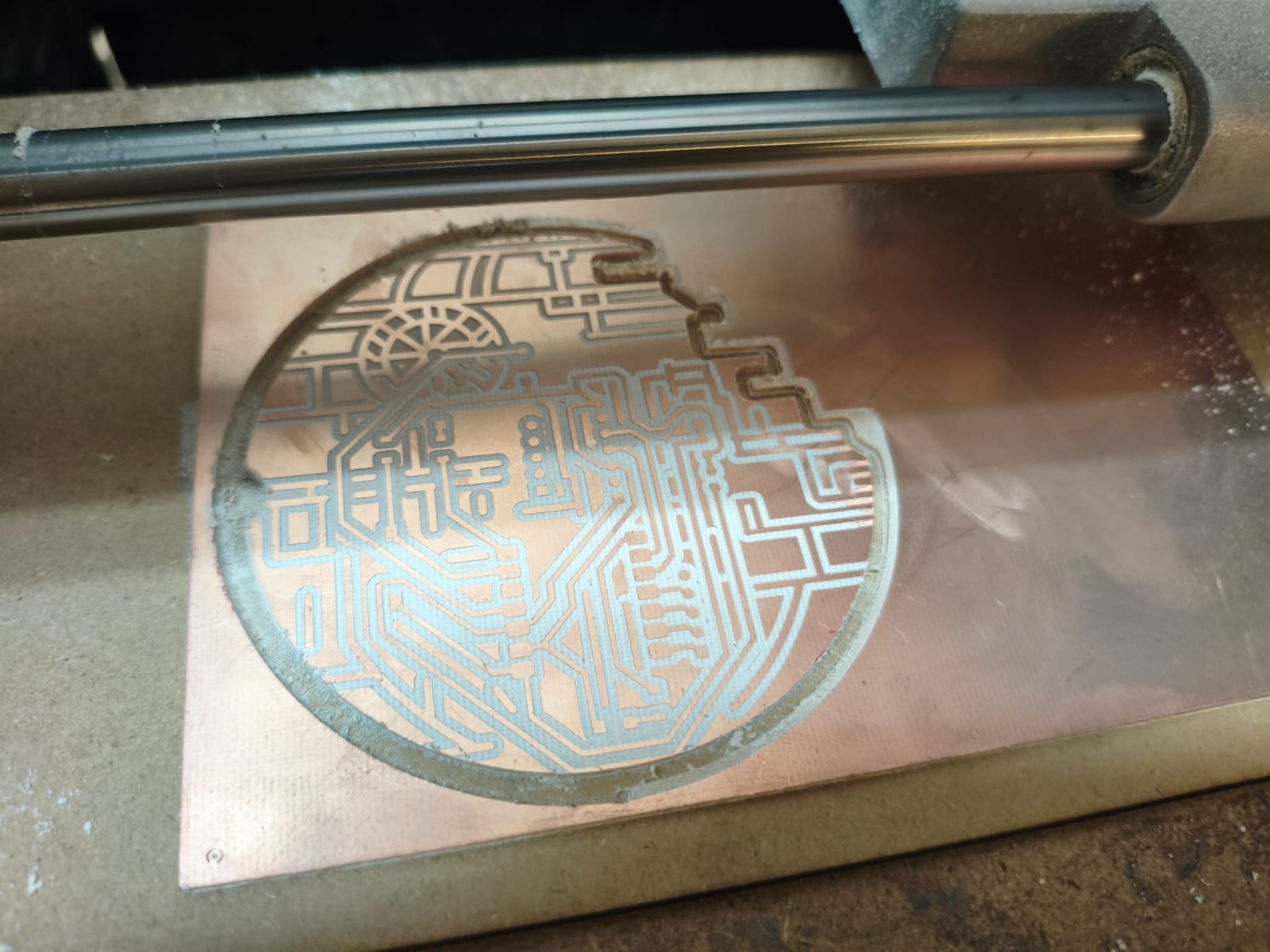
Milling on the Roland Monofab SRM-20
It was time to take our generated files to the machine.
Tooling and Materials
We use copper-clad plates with a fiberglass base. Because we have two different operations, we must use two different tools.
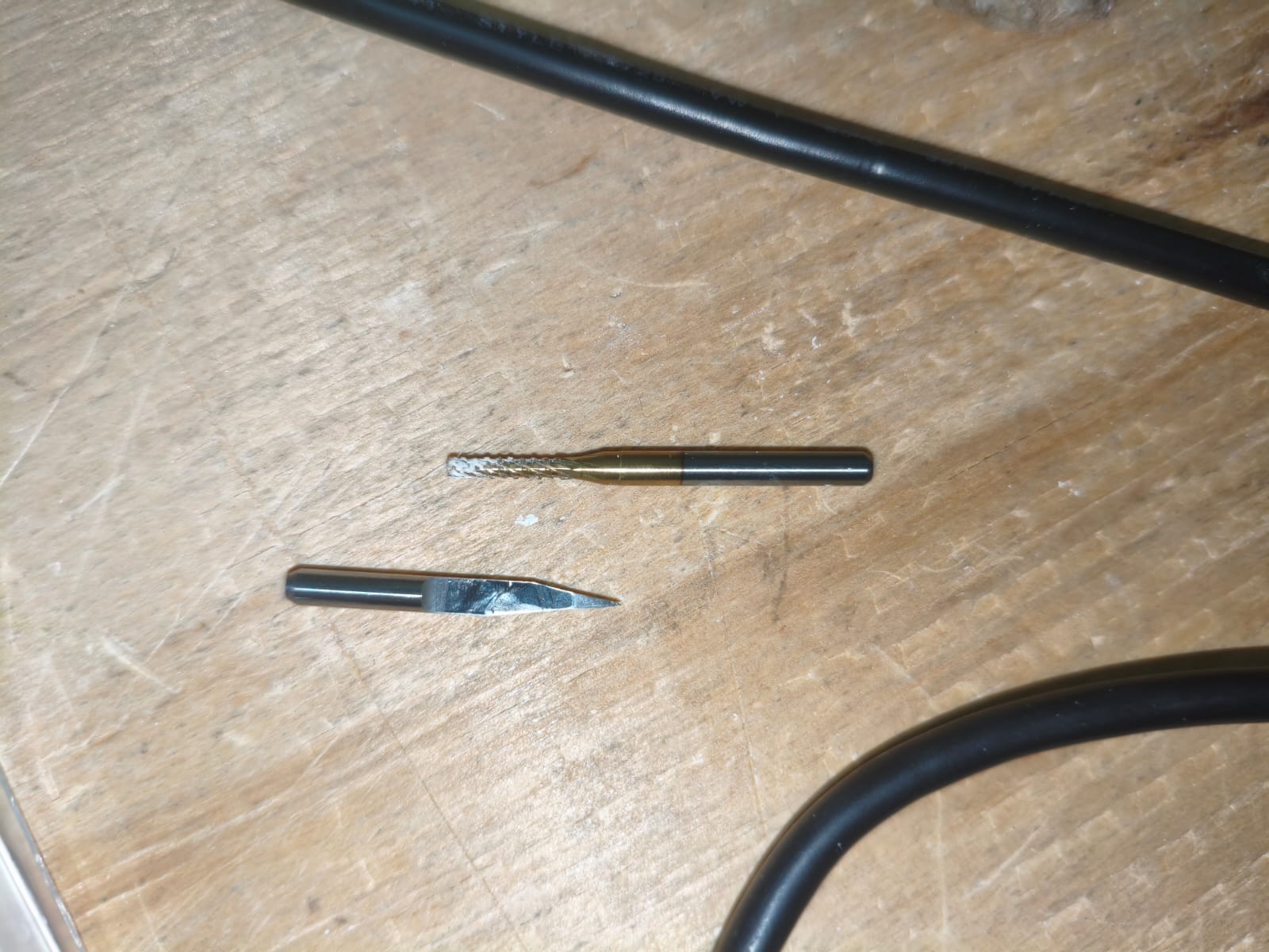
The tools used for the cutting and engraving of the traces.
Operating VPanel
The software used to control the Monofab is VPanel for SRM-20. The interface is extremely straightforward, allowing you to manually jog the spindle, set your X/Y/Z zeroes precisely, and send the output file.
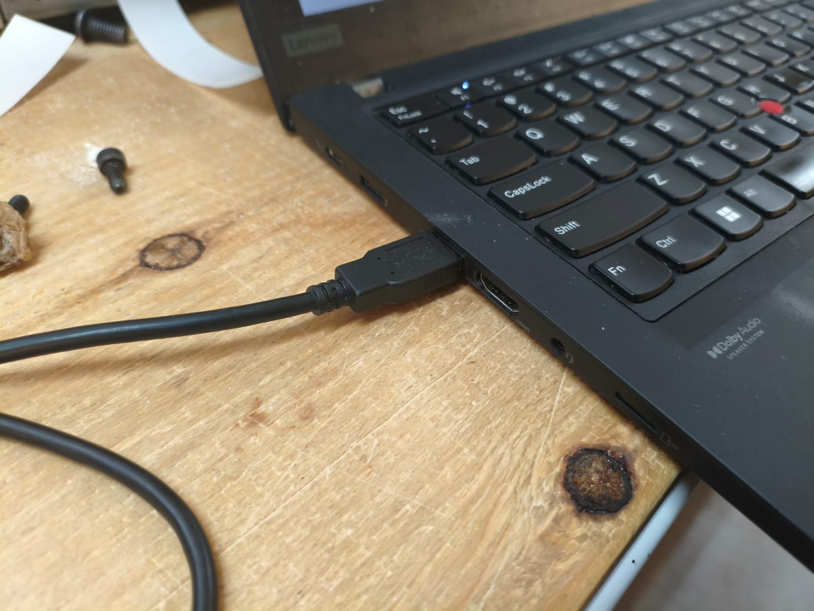
CRITICAL: VPanel streams the G-code directly. You MUST keep the computer connected and awake during the entire cutting process, or the machine will stop mid-job!
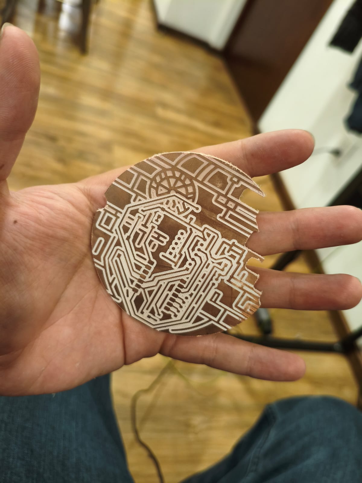
The Milling Process & Final Results
Milling the PCB.
After a successful cut, a bit of cleaning, and manually soldering all my SMD components, here are the hero shots of my finished Death Star board:
Result of soldering
Timelapse of the soldering process.
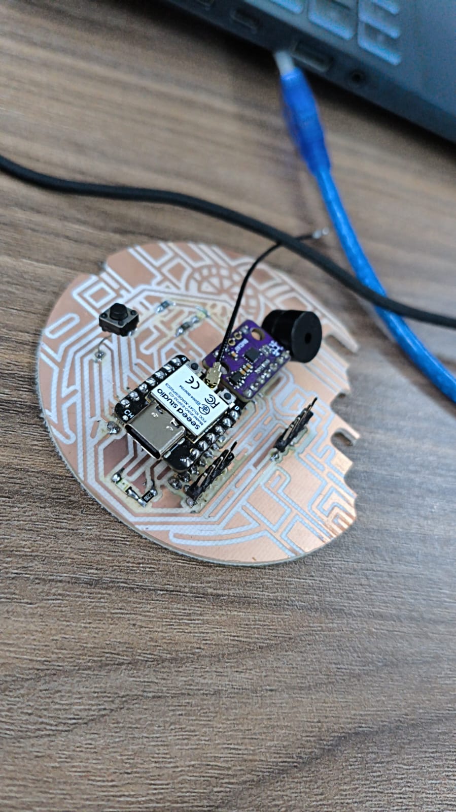
Solder result
Programming the ESP32-C3 & BMI160
To test the microcontroller development board, I needed to ensure my ESP32-C3 could successfully communicate with the onboard BMI160 (an advanced 6-axis IMU/gyroscope) via I2C. I used the ESP-IDF framework and pure C for this implementation.
#include
#include
#include "freertos/FreeRTOS.h"
#include "freertos/task.h"
#include "driver/i2c.h"
#include "esp_timer.h"
#include "esp_err.h"

#define I2C_MASTER_SCL_IO           7
#define I2C_MASTER_SDA_IO           6
#define I2C_MASTER_NUM              0
#define I2C_MASTER_FREQ_HZ          100000
#define I2C_MASTER_TX_BUF_DISABLE   0
#define I2C_MASTER_RX_BUF_DISABLE   0
#define SENSOR_ADDR                 0x68
#define PI                          3.14159265358979323846

static esp_err_t i2c_master_init(void)
{
    i2c_config_t conf = {
        .mode = I2C_MODE_MASTER,
        .sda_io_num = I2C_MASTER_SDA_IO,
        .scl_io_num = I2C_MASTER_SCL_IO,
        .sda_pullup_en = GPIO_PULLUP_ENABLE,
        .scl_pullup_en = GPIO_PULLUP_ENABLE,
        .master.clk_speed = I2C_MASTER_FREQ_HZ,
    };

    i2c_param_config(I2C_MASTER_NUM, &conf);
    return i2c_driver_install(I2C_MASTER_NUM, conf.mode, I2C_MASTER_RX_BUF_DISABLE, I2C_MASTER_TX_BUF_DISABLE, 0);
}

void app_main(void)
{
    ESP_ERROR_CHECK(i2c_master_init());

    uint8_t cmd_reg = 0x7E;

    uint8_t cmd_accel = 0x11;
    uint8_t write_accel[2] = {cmd_reg, cmd_accel};
    i2c_master_write_to_device(I2C_MASTER_NUM, SENSOR_ADDR, write_accel, 2, 1000 / portTICK_PERIOD_MS);
    vTaskDelay(50 / portTICK_PERIOD_MS);

    uint8_t cmd_gyro = 0x15;
    uint8_t write_gyro[2] = {cmd_reg, cmd_gyro};
    i2c_master_write_to_device(I2C_MASTER_NUM, SENSOR_ADDR, write_gyro, 2, 1000 / portTICK_PERIOD_MS);
    vTaskDelay(100 / portTICK_PERIOD_MS);

    uint8_t reg = 0x0C;
    uint8_t memoria[12];

    float angulo_roll_filtrado = 0.0f;
    float angulo_pitch_filtrado = 0.0f;
    uint64_t tiempo_anterior = esp_timer_get_time();

    while (1) {
        esp_err_t err = i2c_master_write_read_device(I2C_MASTER_NUM, SENSOR_ADDR, ®, 1, memoria, 12, 100 / portTICK_PERIOD_MS);

        if (err == ESP_OK) {
            uint64_t tiempo_actual = esp_timer_get_time();
            float dt = (tiempo_actual - tiempo_anterior) / 1000000.0f;
            tiempo_anterior = tiempo_actual;

            int16_t gyro_x_raw = (memoria[1] << 8) | memoria[0];
            int16_t gyro_y_raw = (memoria[3] << 8) | memoria[2];

            int16_t accel_x_raw = (memoria[7] << 8) | memoria[6];
            int16_t accel_y_raw = (memoria[9] << 8) | memoria[8];
            int16_t accel_z_raw = (memoria[11] << 8) | memoria[10];

            float gyro_x_rate = gyro_x_raw / 16.4f;
            float gyro_y_rate = gyro_y_raw / 16.4f;

            float g_x = accel_x_raw / 16384.0f;
            float g_y = accel_y_raw / 16384.0f;
            float g_z = accel_z_raw / 16384.0f;

            float accel_roll = atan2(g_y, g_z) * (180.0 / PI);
            float accel_pitch = atan2(-g_x, sqrt(g_y * g_y + g_z * g_z)) * (180.0 / PI);

            angulo_roll_filtrado = 0.98f * (angulo_roll_filtrado + gyro_x_rate * dt) + 0.02f * accel_roll;
            angulo_pitch_filtrado = 0.98f * (angulo_pitch_filtrado + gyro_y_rate * dt) + 0.02f * accel_pitch;

            printf("Roll: %.2f \t Pitch: %.2f\n", angulo_roll_filtrado, angulo_pitch_filtrado);
        } else {
            printf("I2C error (ret=%d)\n", err);
        }

        vTaskDelay(20 / portTICK_PERIOD_MS);
    }
}
Result
Files
Here you can download the original DXF vector files I generated for this furniture project: