

Week 06
Electronics Design
// MAIN OBJECTIVE \\
The primary goal of this week is to create a digital PCB, establishing the basics to implement components for my future final project. This involves selecting basic parts, resolving software library issues, and navigating the complete workflow from schematic to 3D simulation to prepare for physical milling.
If you want to see our Group Assignment for this week, click HERE →
What is a PCB?
A Printed Circuit Board (PCB) is the foundational building block of most modern electronic devices. It structurally supports and electrically connects electronic components using conductive tracks, pads, and other features etched from copper sheets laminated onto a non-conductive substrate. Designing our own PCBs allows us to transition from messy breadboard prototypes to reliable, permanent circuits.
Components
For this initial design, I kept the architecture basic but forward-looking. These components were chosen specifically because they will be extremely useful later on for integrating sensors and controlling flight parameters on my drone project:
- Seeed Studio XIAO ESP32C3: A powerful tiny microcontroller with built-in Wi-Fi and Bluetooth, perfect for wireless communication and processing sensor data.
- Push Button: A simple tactile switch for user input and testing.
- LED: A status indicator essential for visual feedback.
- Pin Headers: Used with jumpers to easily connect and test various external sensors down the line without needing a new board design every time.
Designing with Altium
To design the PCB, I utilized Altium Designer →, a professional grade PCB and electronic design automation software. Its potential lies in its unified environment, allowing you to seamlessly move from schematic capture to PCB layout, routing, and 3D simulation within a single platform.
The Interface
The Altium interface is complex but highly structured. You can manage projects on the left panel, design in the central workspace, adjust properties and import parts on the right. Switching between 2D layout and 3D visualization is smooth, providing an excellent perspective on how the final physical board will look.
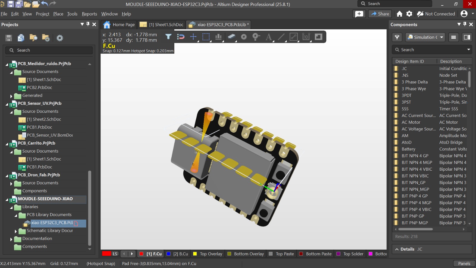
The Altium Designer interface.
The principal problem
When starting the schematic, I encountered a significant issue: there was no importable and simulatable model of the XIAO ESP32C3 available directly for Altium. I attempted to use the KiCad import wizard to bring the model over, but it incorrectly generated a normal board project (.PrjPcb) instead of the required library package (.LibPkg).
The Solution
To fix this, I had to manually repackage the library components so Altium could read them correctly as a unified part.
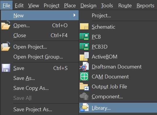
First, I created a new Integrated Library project (.LibPkg).
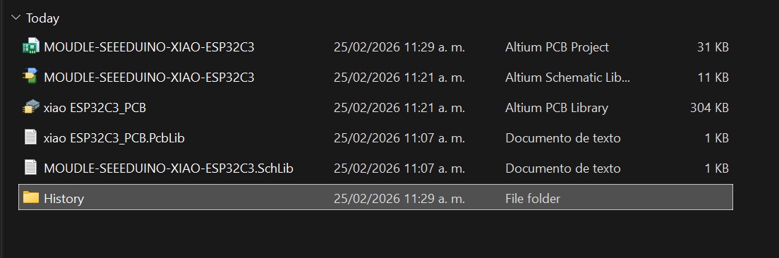
Next, I dragged the previously generated schematic library (.SchLib) and PCB library (.PcbLib) files into this new container.
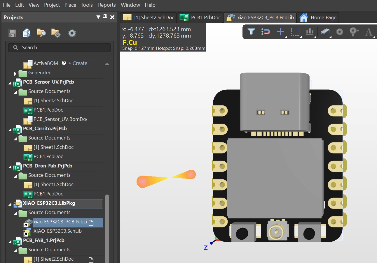
Finally, I compiled the new project to generate the Integrated Library file, making the XIAO ESP32C3 component fully functional and ready to drop into the schematic.
PCB Creation Process
With the component libraries sorted out, I followed a structured workflow that you can see to create the 3D PCB:
- Schematic Capture: Placed the XIAO ESP32C3, LED, button, and pin headers, wiring them together logically to define the electrical connections.
- Exporting to PCB: Updated the PCB document from the schematic, importing all footprints and connections into the layout editor.
- Routing and Placement: Carefully positioned the components to minimize trace length and manually routed the copper traces to connect the pads.
- 3D Simulation: Switched to the 3D view to verify clearances, check component heights, and ensure the board looked exactly as intended.
Timelapse documenting the layout and routing of the PCB.
Hero Shots
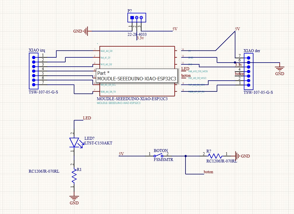
Final schematic with all logical connections.
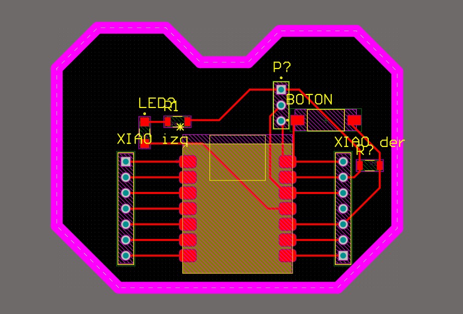
The completed 2D PCB layout with routed traces.
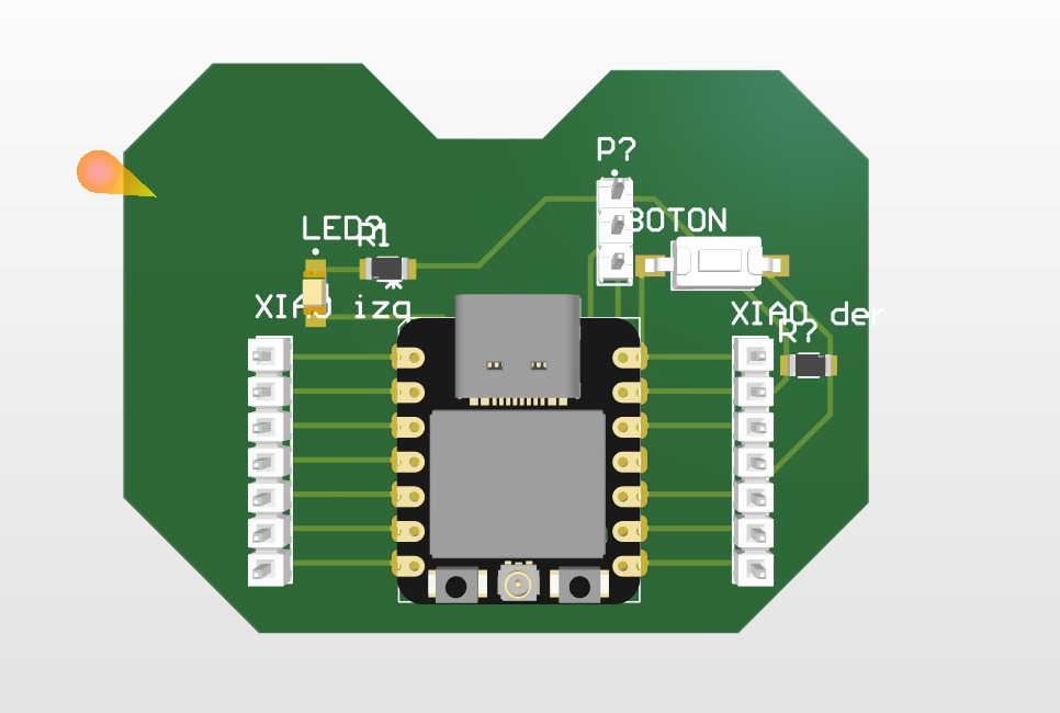
Rendered 3D simulation of the final board.
Extras: Preparing for Milling
To manufacture this board using a Roland Monofab, the digital layout needs to be exported as a PDF. This PDF is then vectorized to generate the cutting toolpaths. Here is the visual process for preparing that export file:
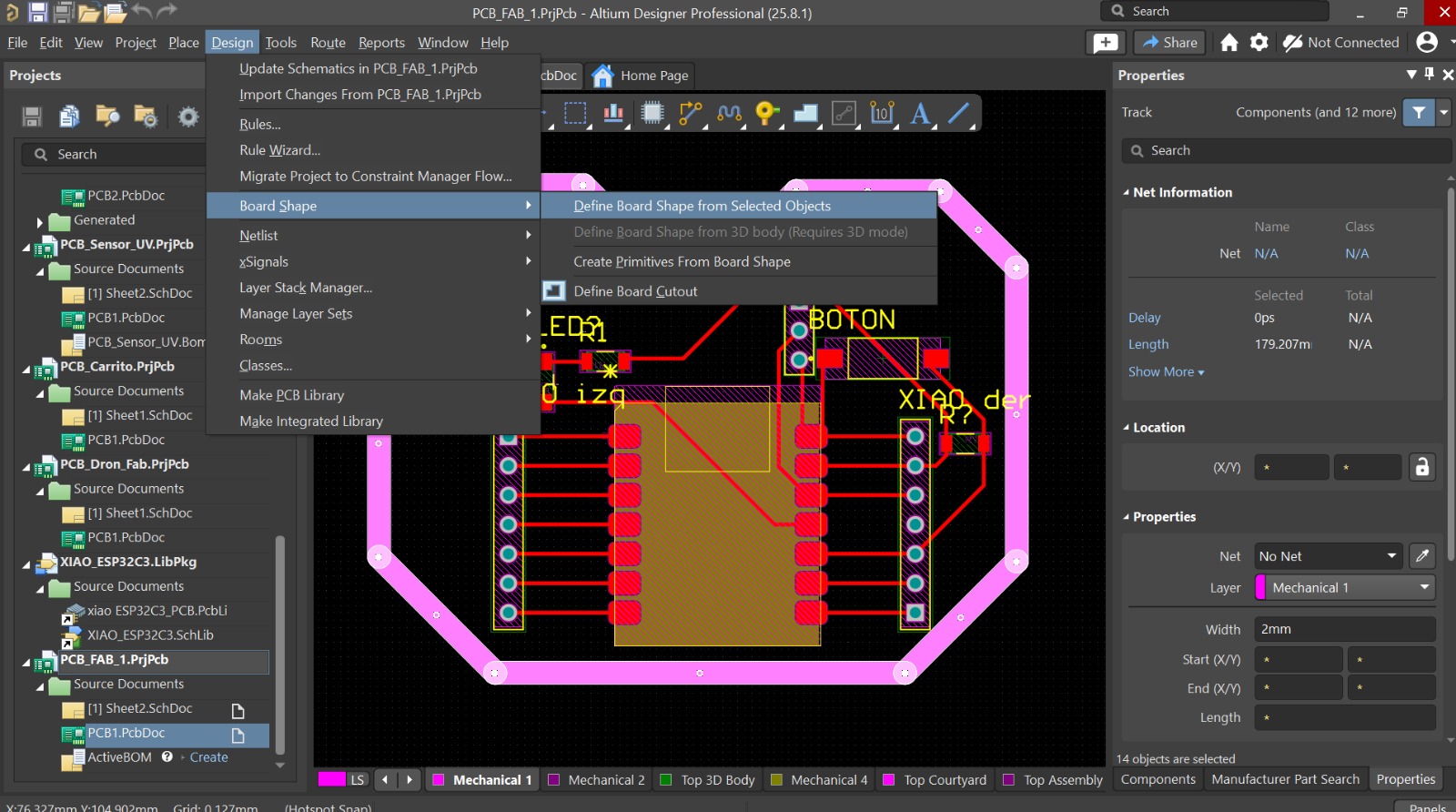
Defining the exact mechanical borders and origin for the board outline.
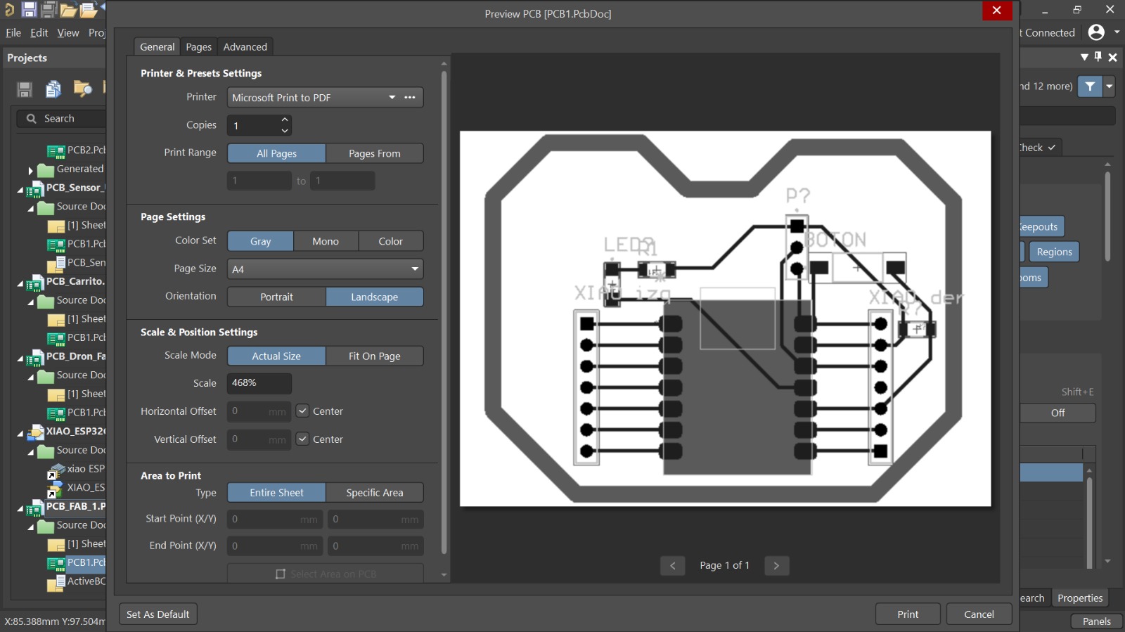
Accessing the Print configuration menu with Ctrl+P .
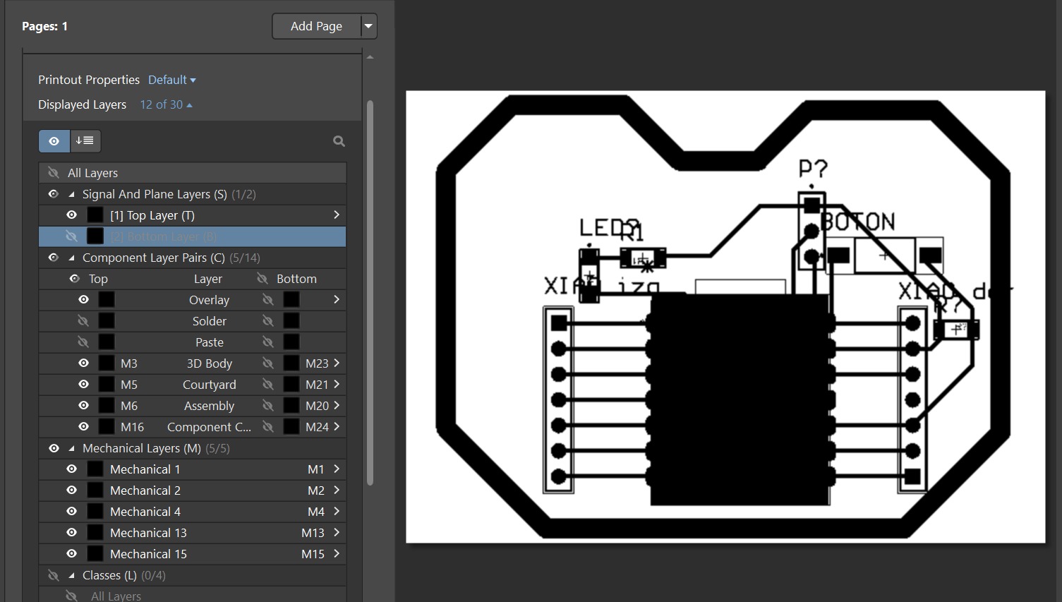
Before: All visible layers in monochromatic configuration.
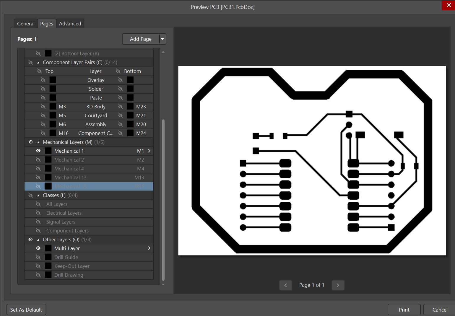
After: Hiding unnecessary layers so only the Top Copper and Keep-Out layer remain for cutting.
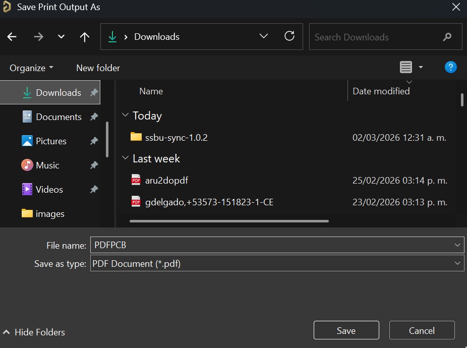
Exporting the final high resolution PDF document.
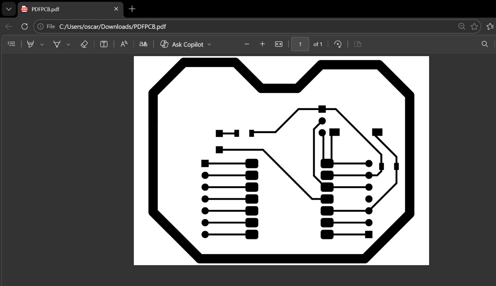
The final generated PDF, ready to be vectorized and sent to the Monofab machine.
Conclusion
This week taught me the immense value of prototyping PCB for my future electronic proyects. I now undestand how to use electronic designing software, handle Kikad schematic and 3D designs for importing them to Altium, and create PDF archives for making the physical PCB. I will be directly implementing these achievments into my Final Project → to design and my PCB for my handmade drone.
Files
Here you can download the original schematic, PCB and PDF files I used for this week's assignments: