8. Electronics production
Group AssignementThis week I learned different options for bringing electronic design to life. Now I know that this came be done through several methods... some more sustainable than others. This processes can use mills, chemicals or blades to give shape to our PCB before all components are soldered on them. Another process that requires some practice.
Some of of my learnings:
- Unfortunately it is not that fast and easy to find SMD components in my city.
- Copper tape and a mini plotter can do magic with a bit of creativity, care and several tests.
- There are many options for PCB production, but the information about it is all scatered.
- The only PCB mill available at my campus is not very easy to access.
- It is VERY important to find the right footprints and schematics before production.
- If the right footprints and schematics are not available, it is always possible to create them.
- Both woftware and hardware have to communicate and be compatibl, so always double-check details.
- Planning the design digitally as well as posible helps, but bringing the design to reality ALWAYS comes with its own challenges.
- Always be prepared to iterate.
Routing on campus
My first attempt to tackle this assignement was about milling a copper board at my campus' labs. I went around asking for the place and person that could help me only to find out it has a waiting list protocol and students are not normally involved in the process. I'm still waiting on the permission and scheduling of my turn. (One week later)
This is the lab and forms I am talking about.
*I came back later for my final project and was able to mill my pcb! Go to the end of this page to see the process and results.
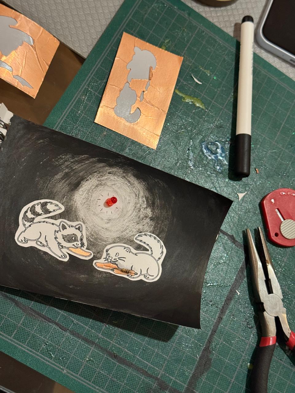
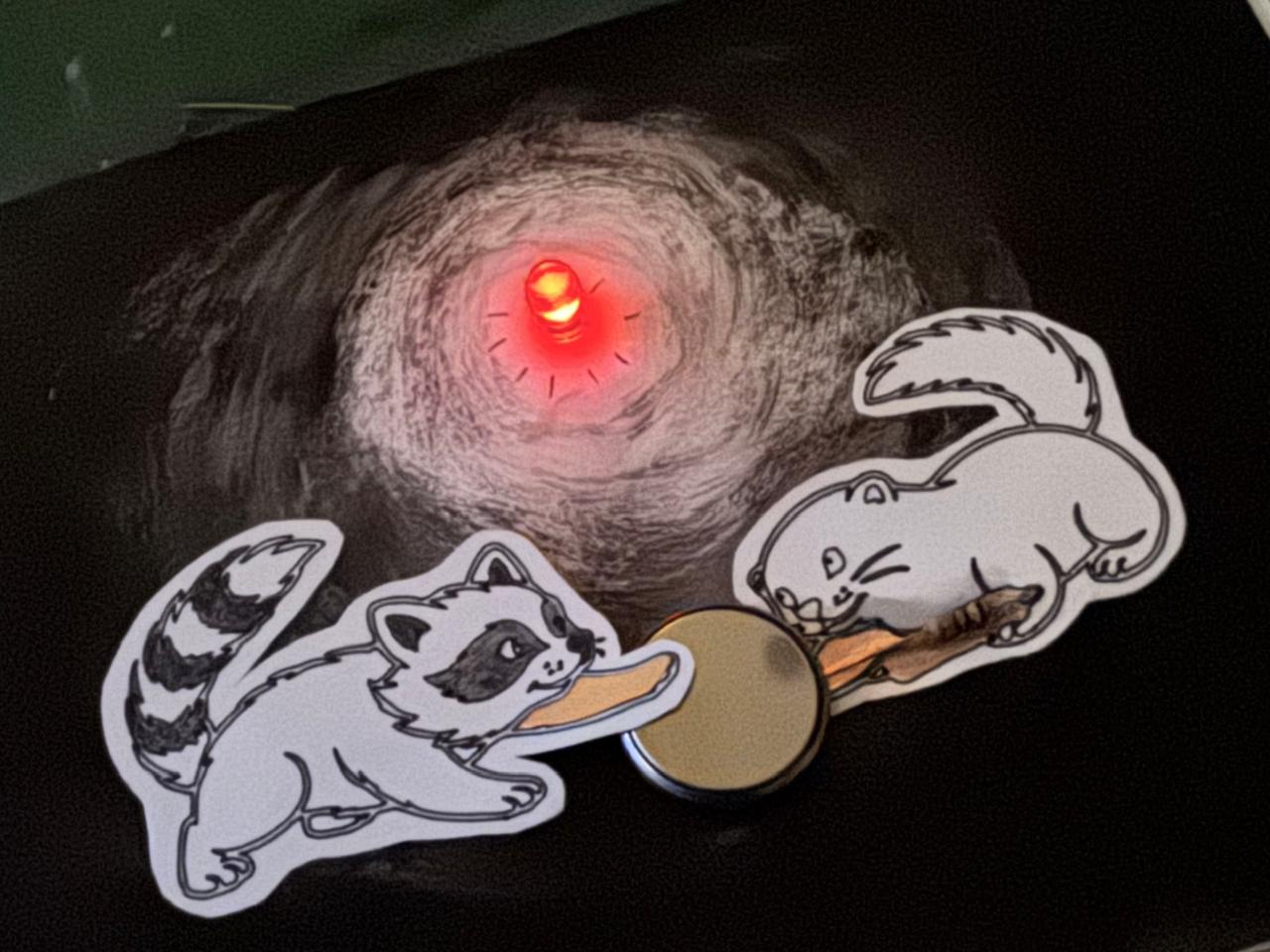
Tape test (mini project)
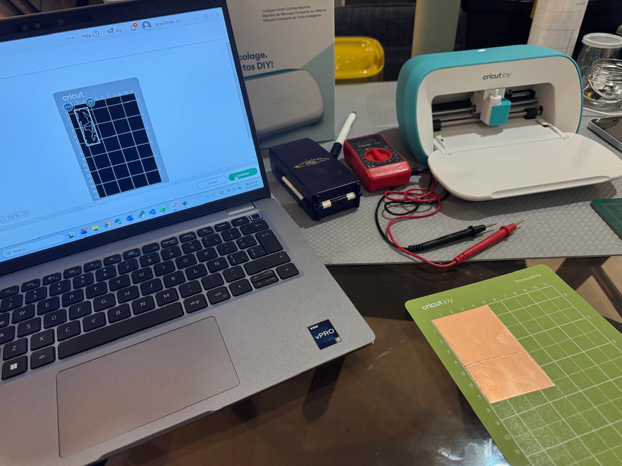
As a second attempt I tried getting copper tape and using a plotter. Before soldering anything or adding a microcontroler, I decided to test a very simple circuit to see if the tape worked. I had so much fun with this mini project:
- First things first: testing the conductivity and connections for the mini project. (Coin battery, copper tape, resistor and LED)
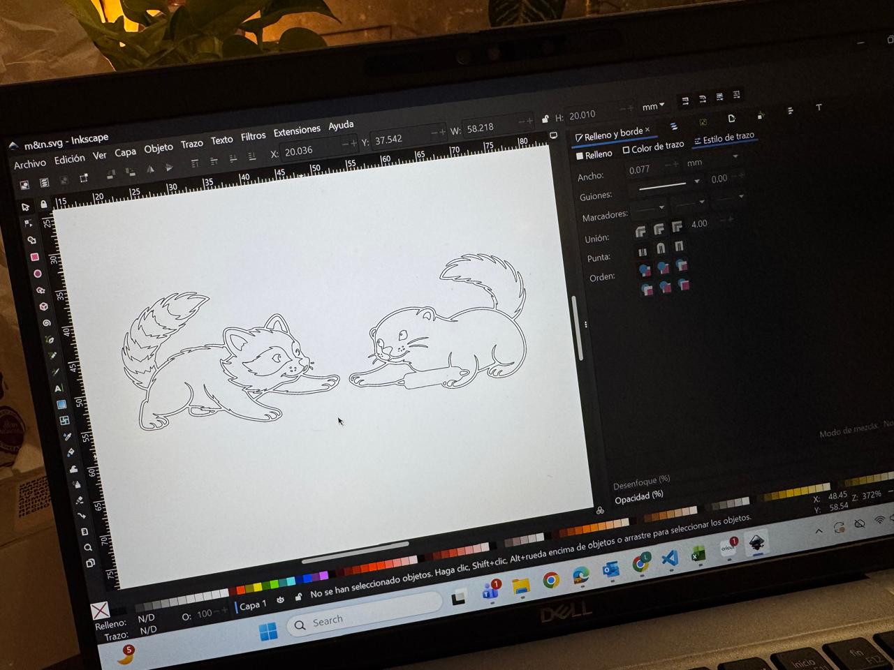
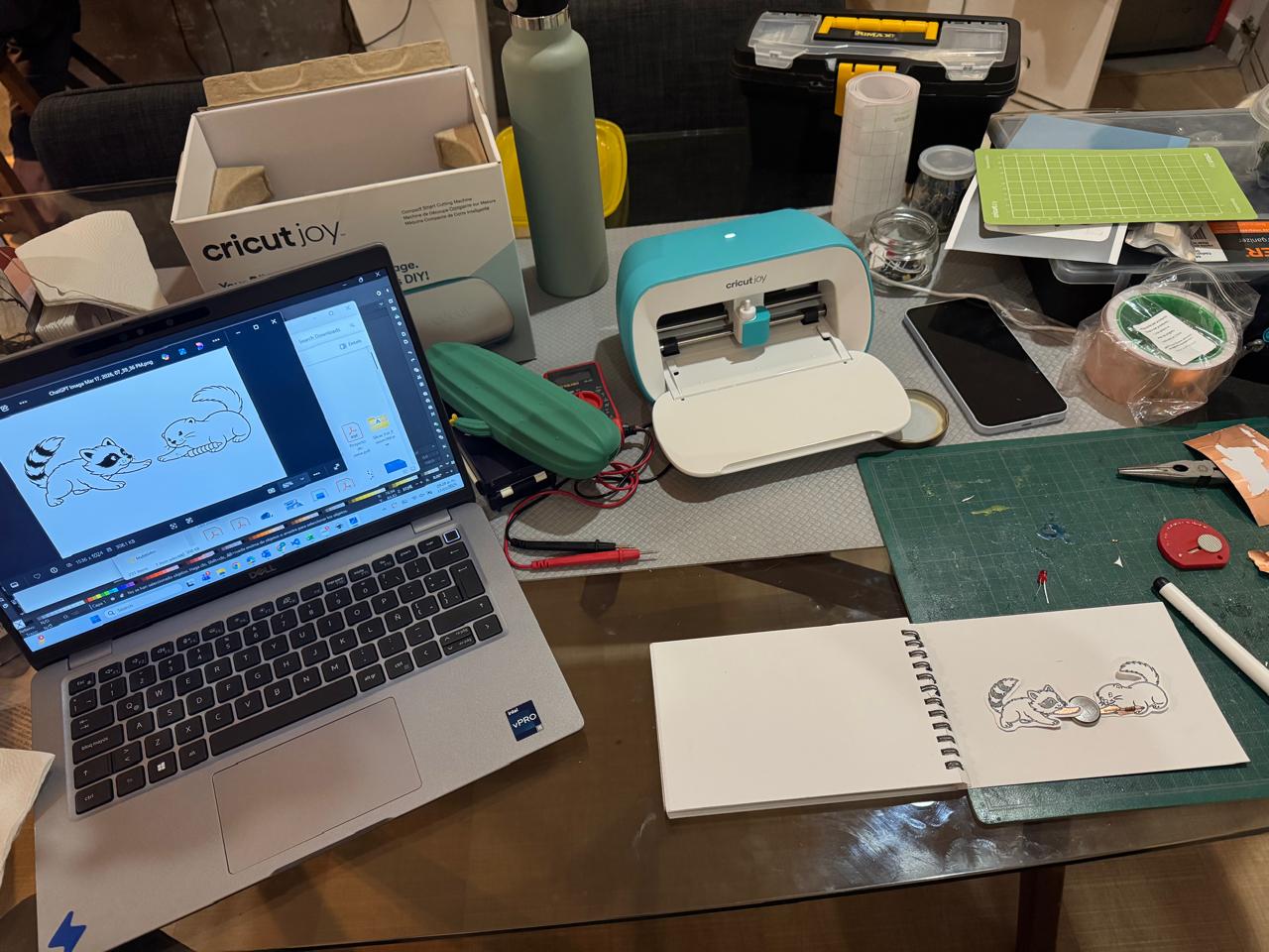
- Then I made an sketch that would give this circuit a personality
- I printed the sketch with a marker in the plotter (first time ever doind this)
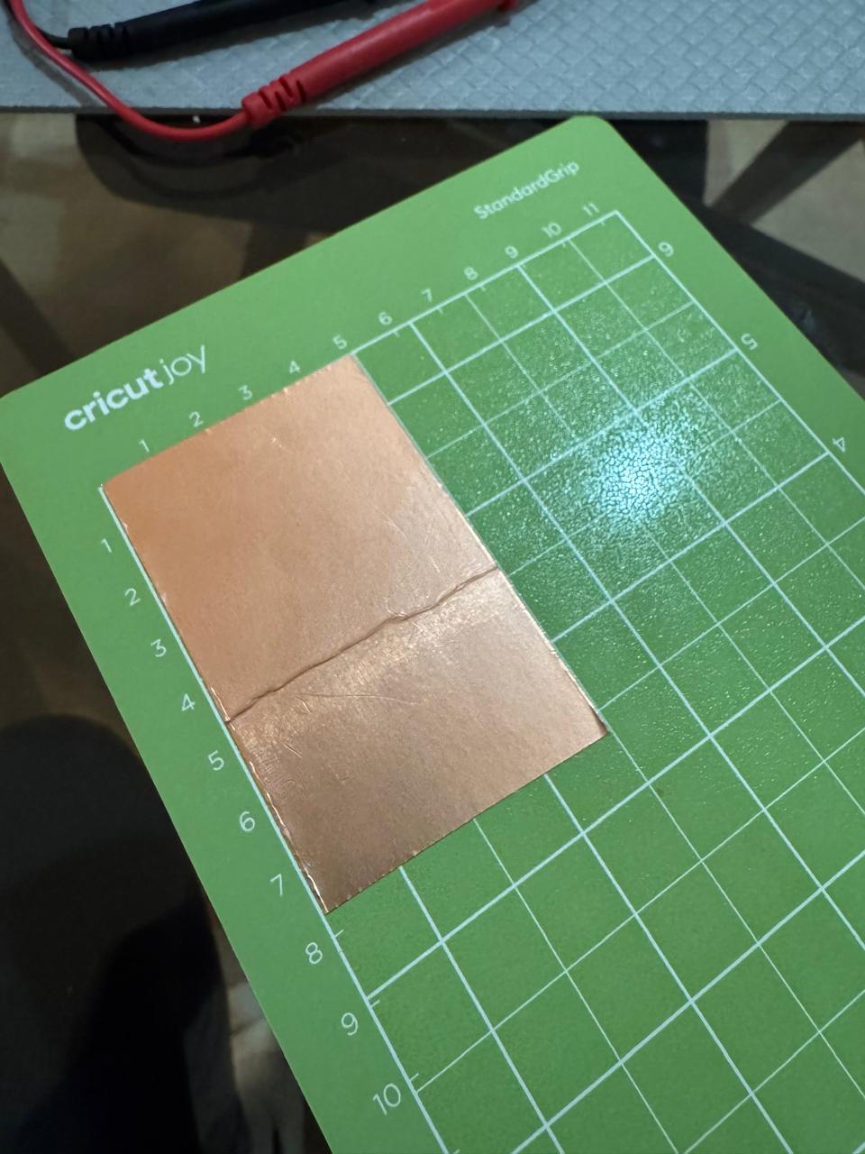
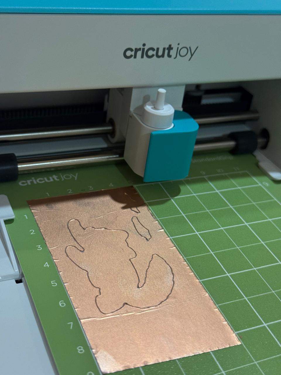
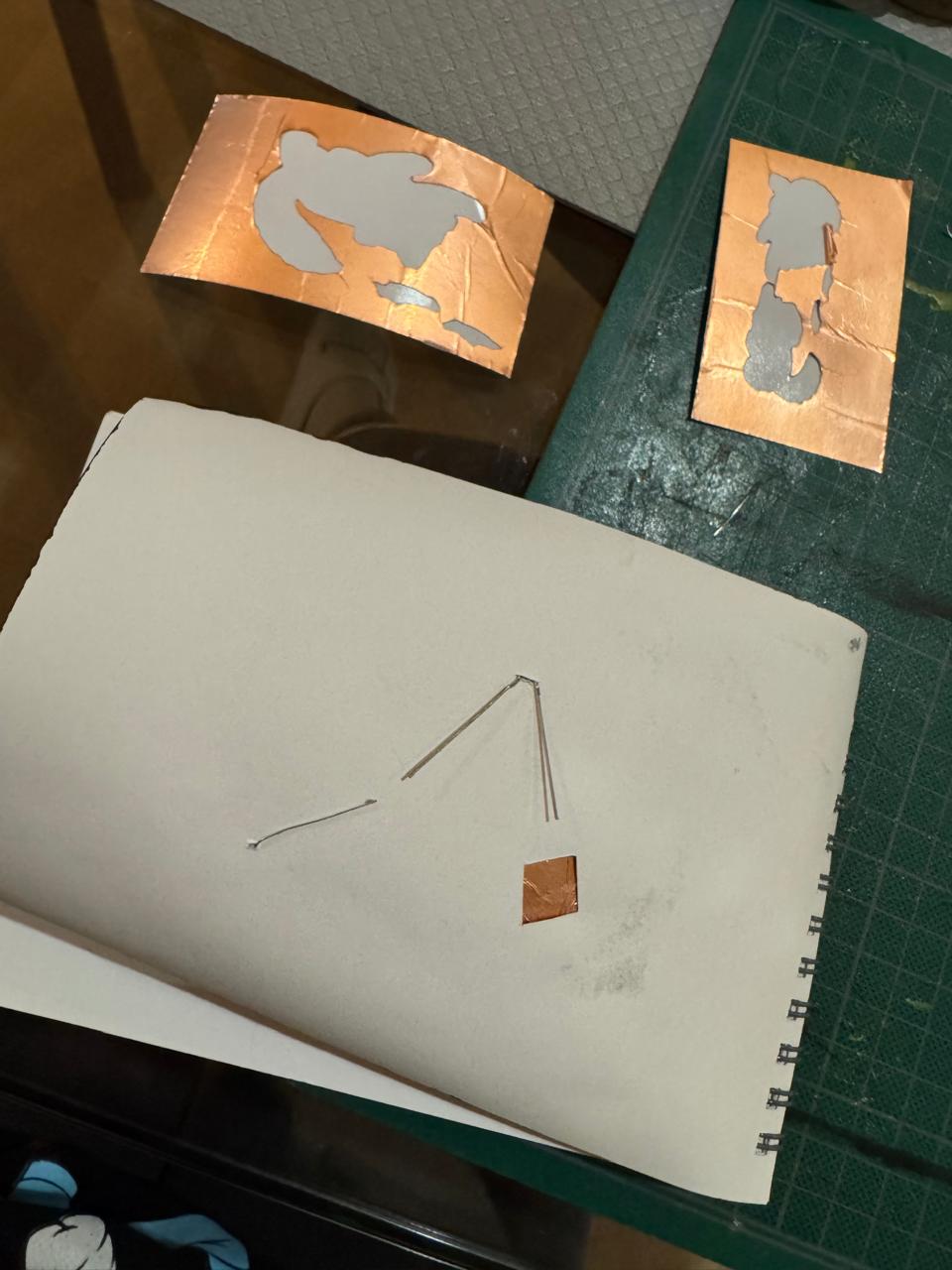
- The next step was to prepare the copper and the design for it
- The first cut wasn't so good because I didn't choose the material right. At least this cut worked to test size and shapes.
- I realized I had to make everything bigger and further appart, so I made the necessary adjustments:
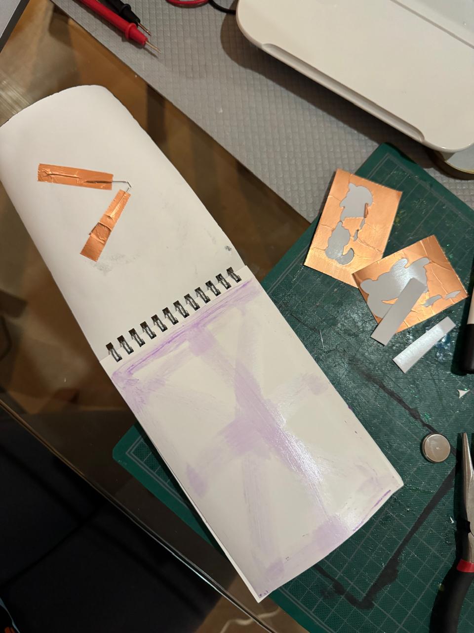
- For the following copper cut I did choose the right material
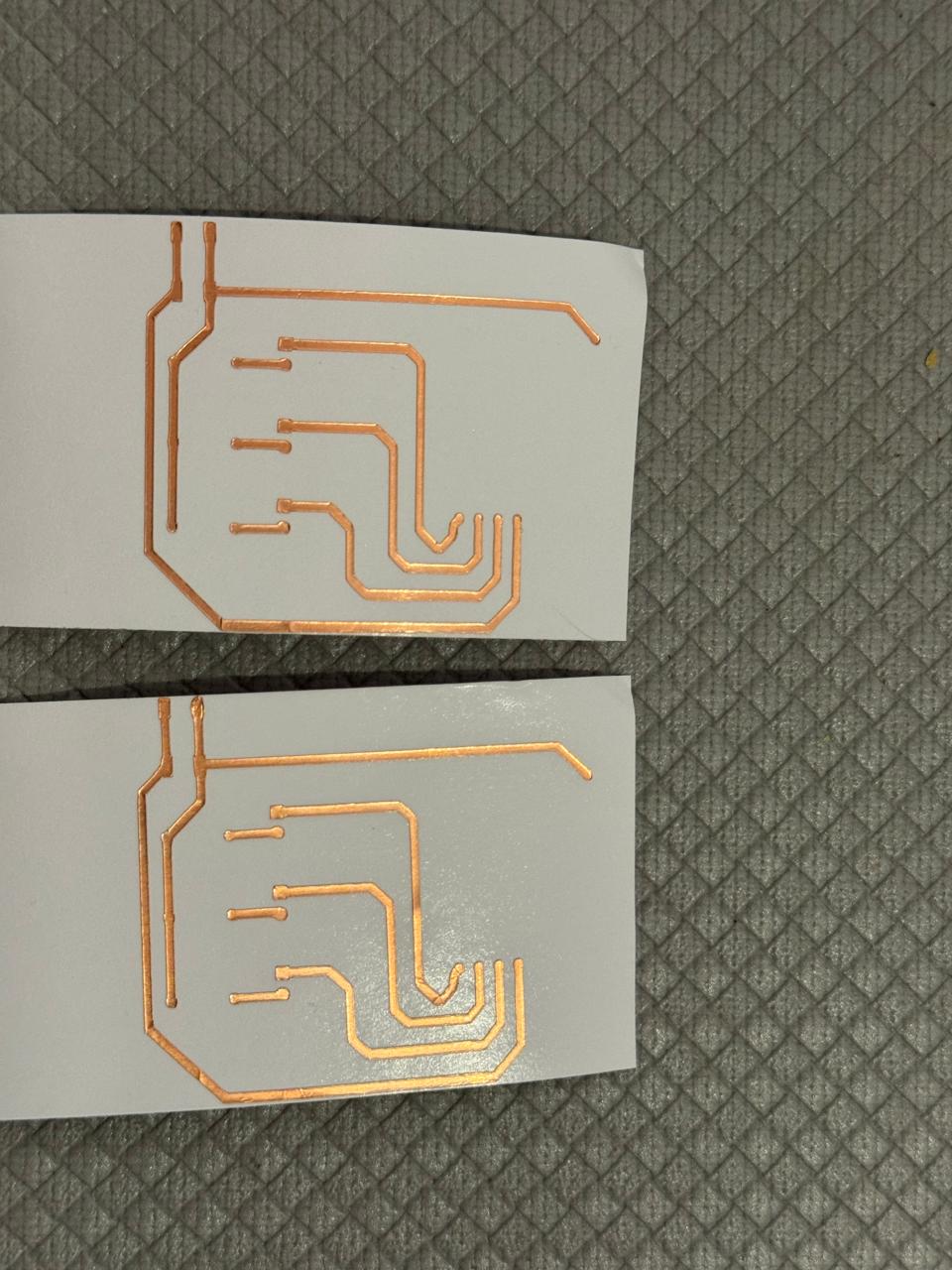
- It felt like a background was missing, so I quickly painted one by hand and started pasting everything in place
- I am so happy with the final outcome:
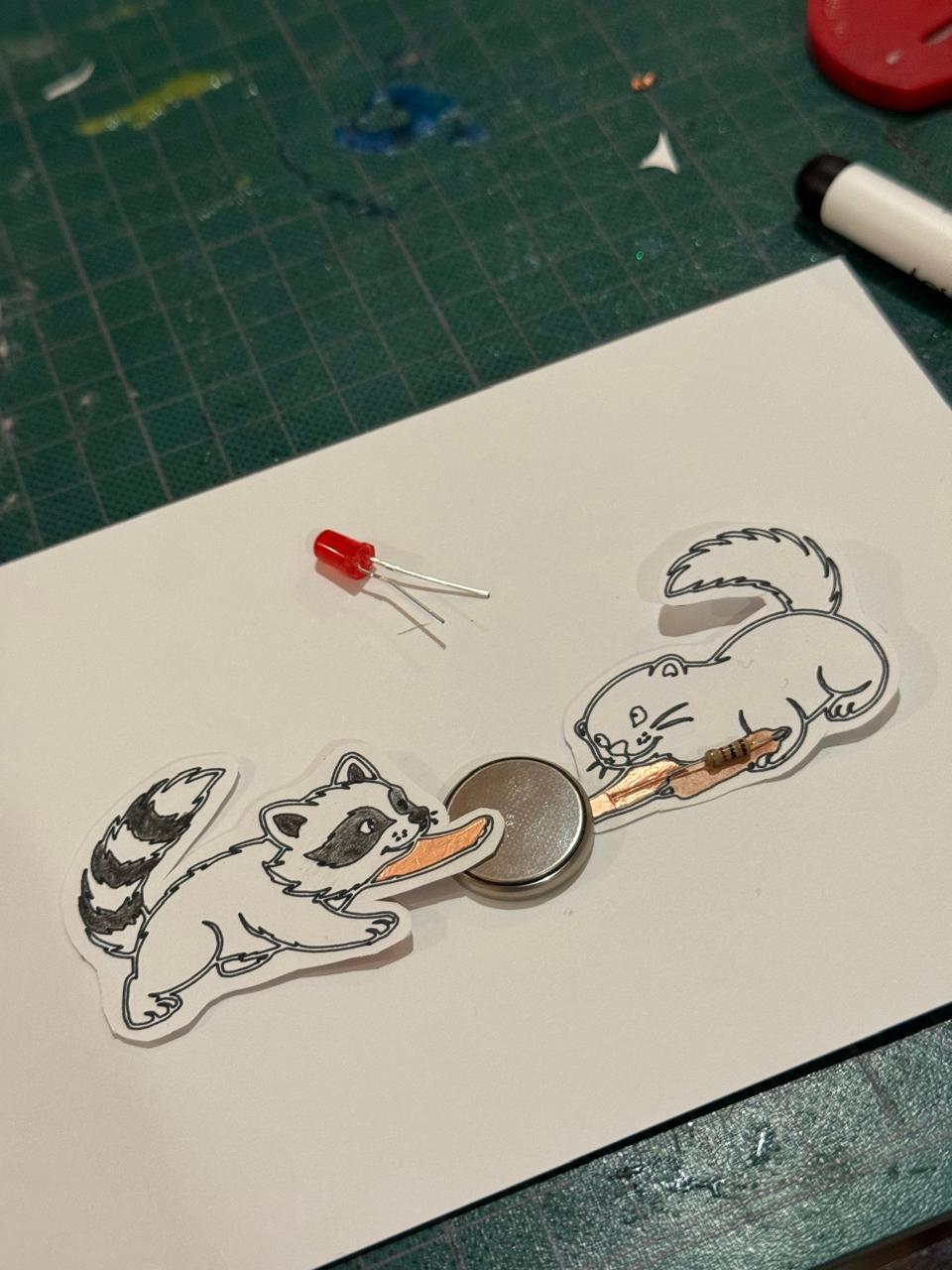
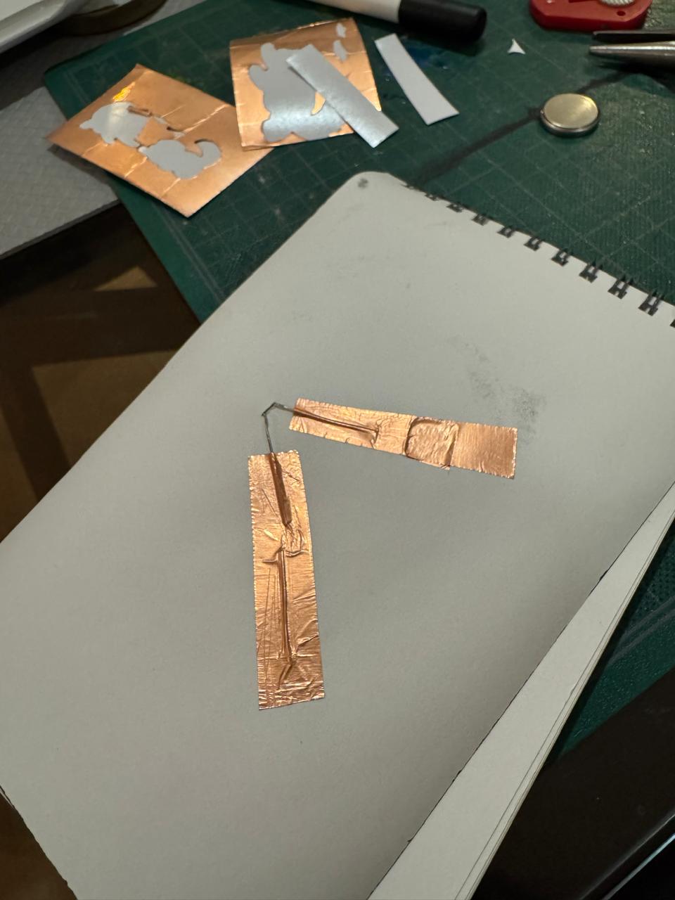
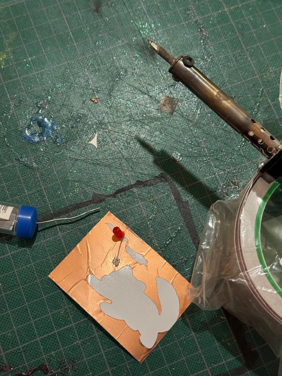
Besides the mini project, I checked that soldering over the tape wouldn't be a problem and fortunately it works well:
PCB Production with Plotter
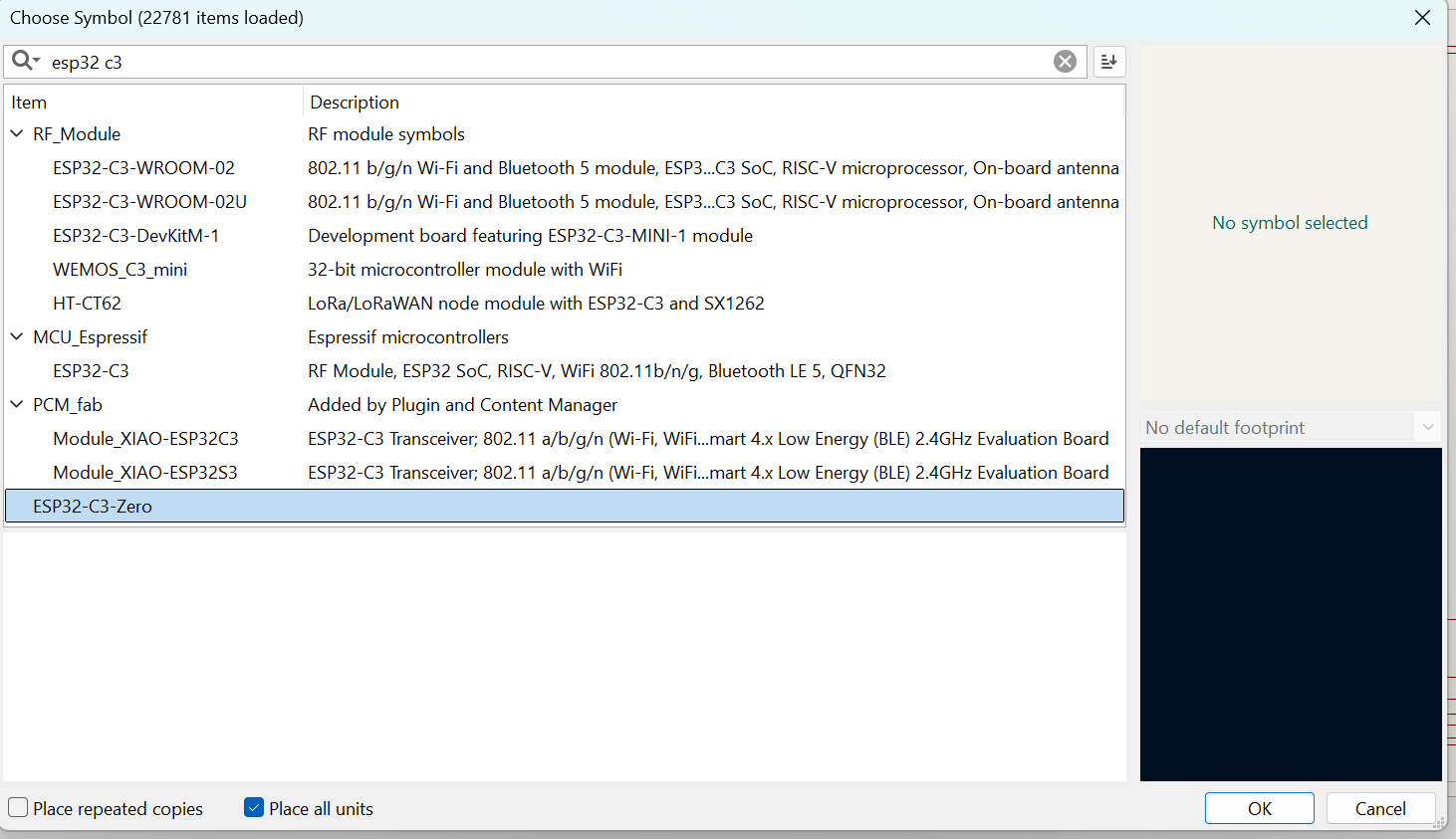
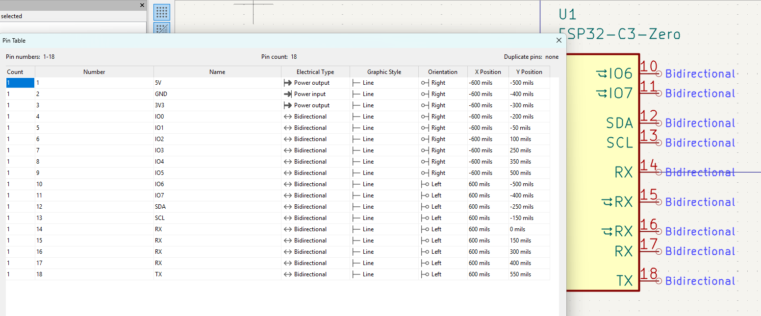
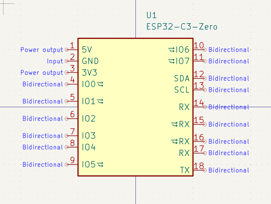
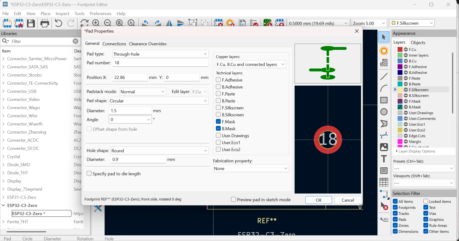
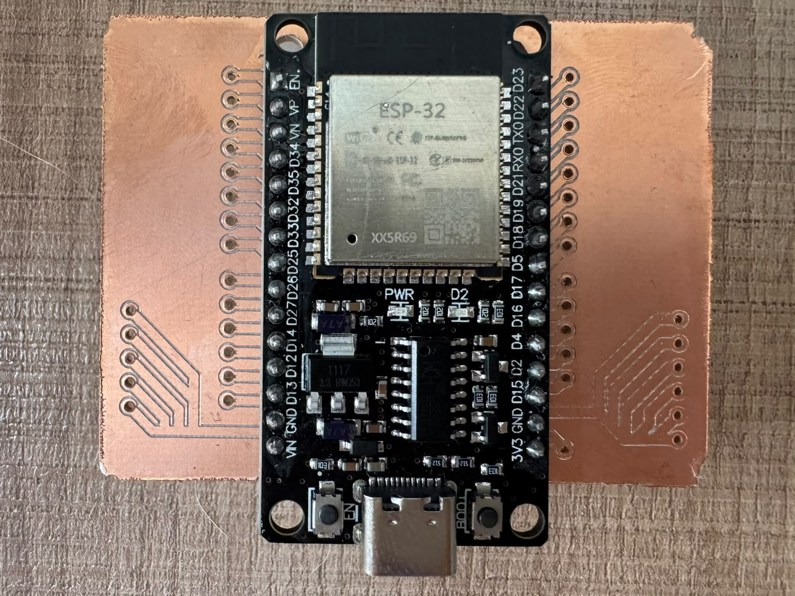
Now the next step is finding the right footprint and schematic for the microcontroler I was able to get: ESP32-C3-Zero.
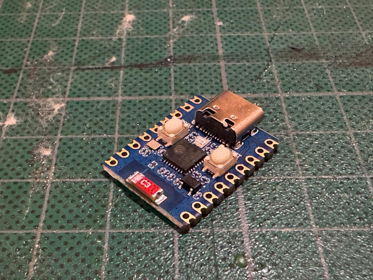
Here is some useful information about it:
I wasn't able to find the schematic or footprints for this exact microcontroler :( So I asked ChatGPT if it could help me create them:
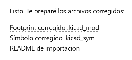
Although it seemed like files were created and I was able to upload them to KiCad, when I tried using them nothing showed up:
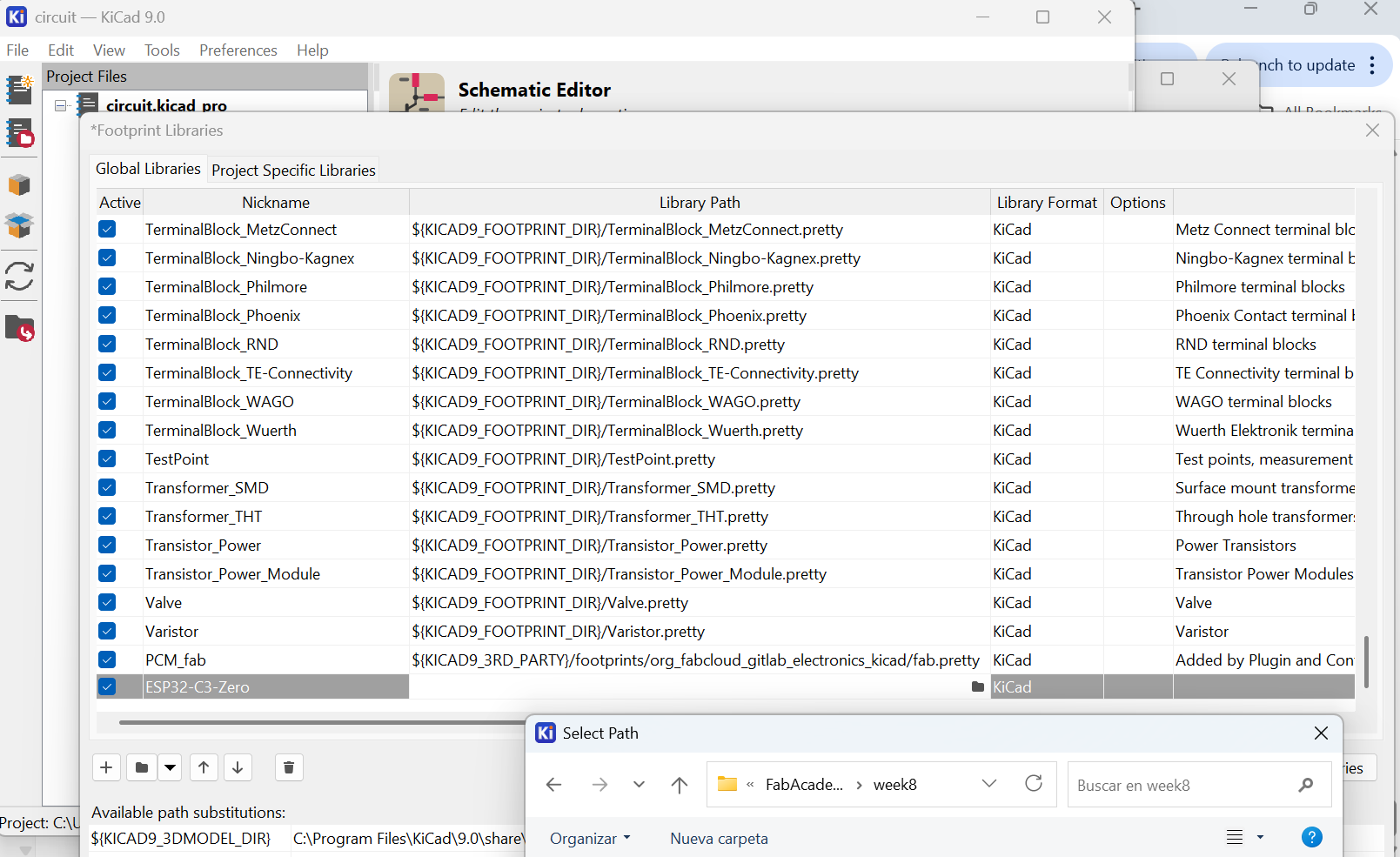
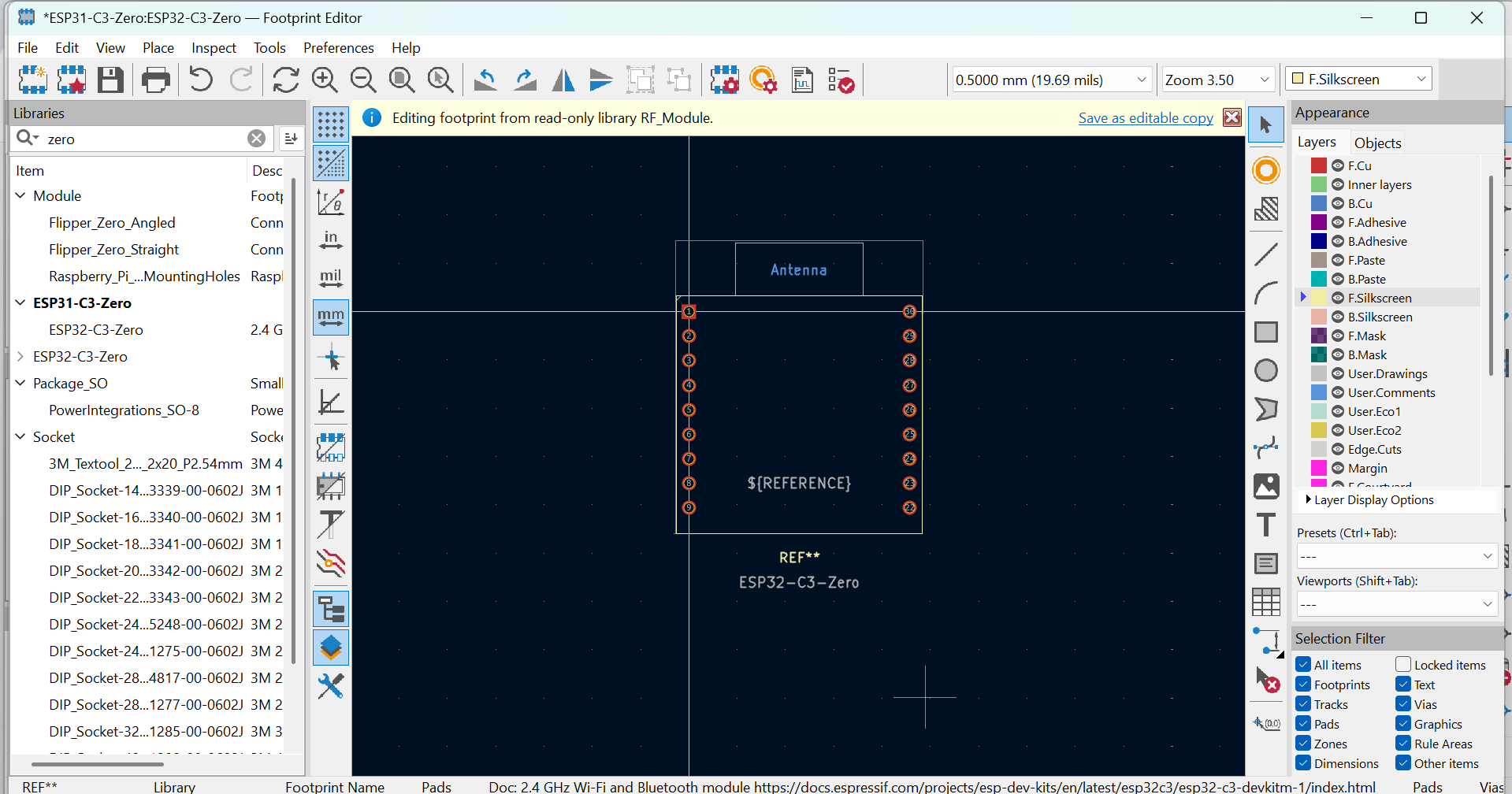
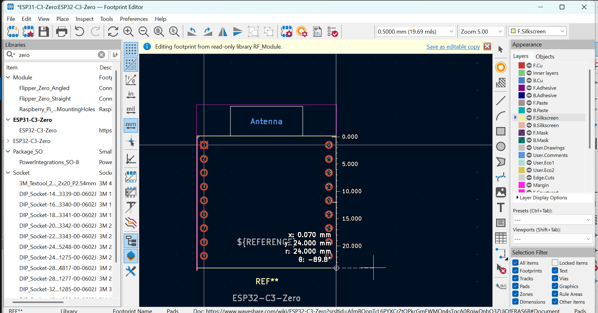
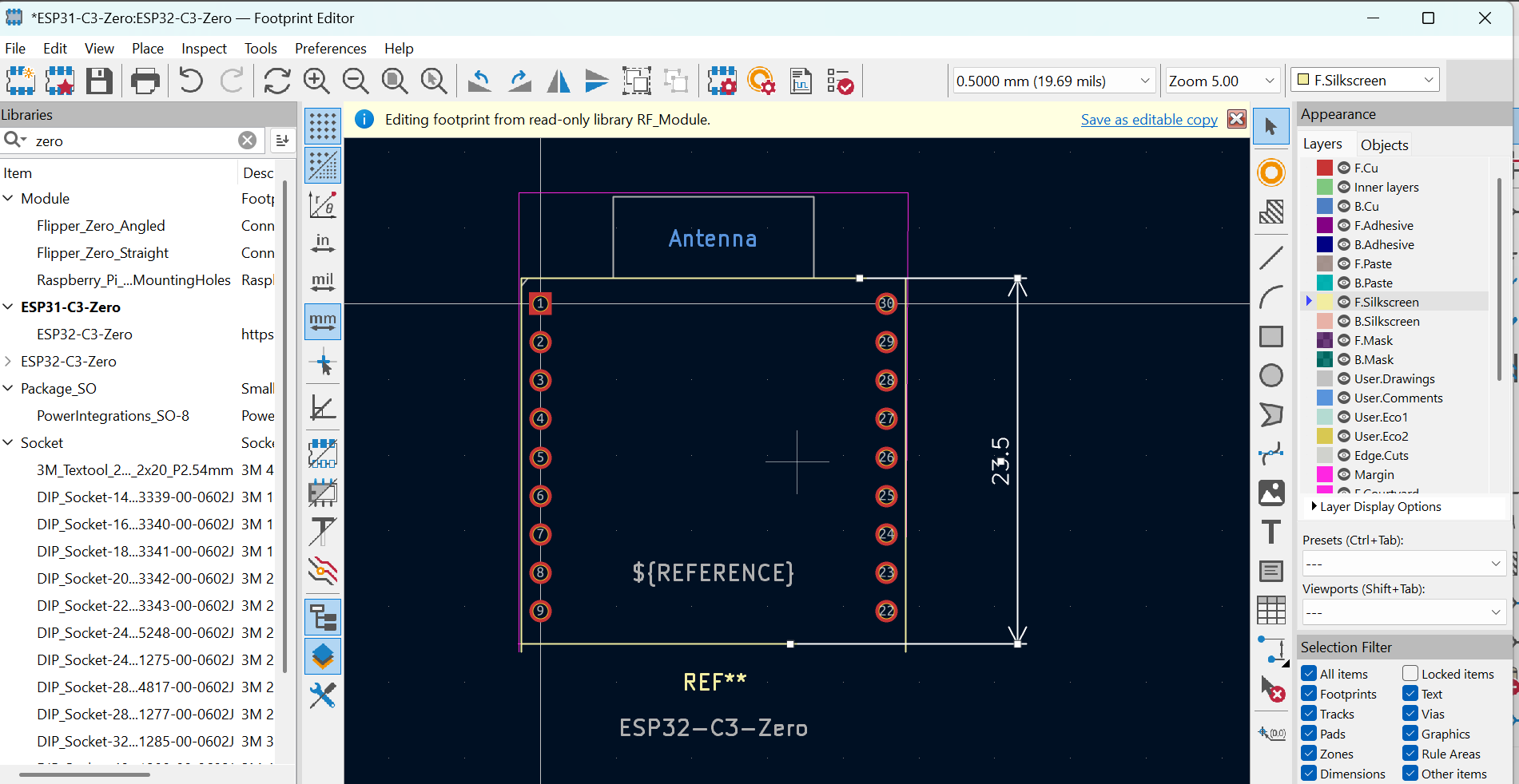
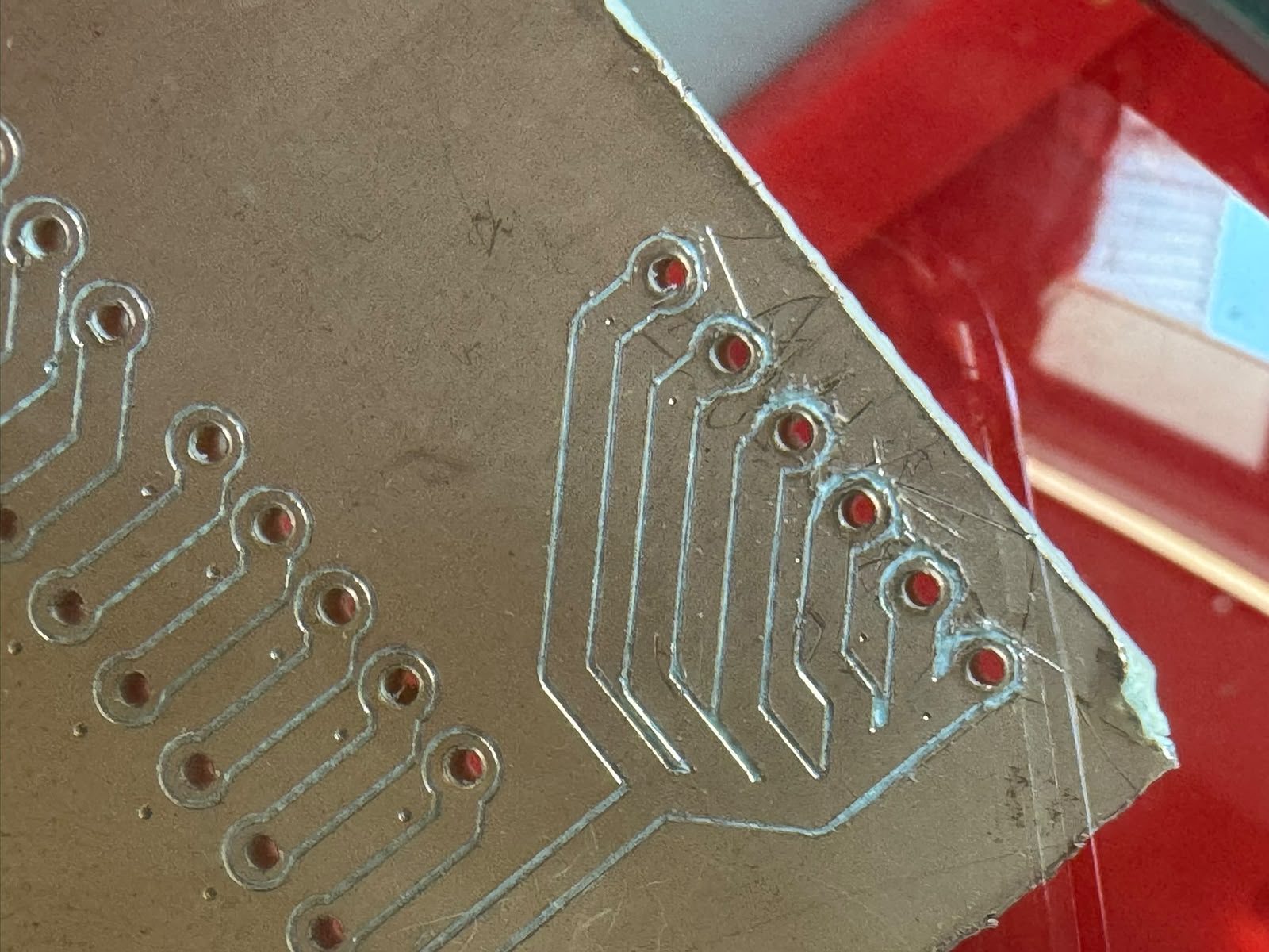
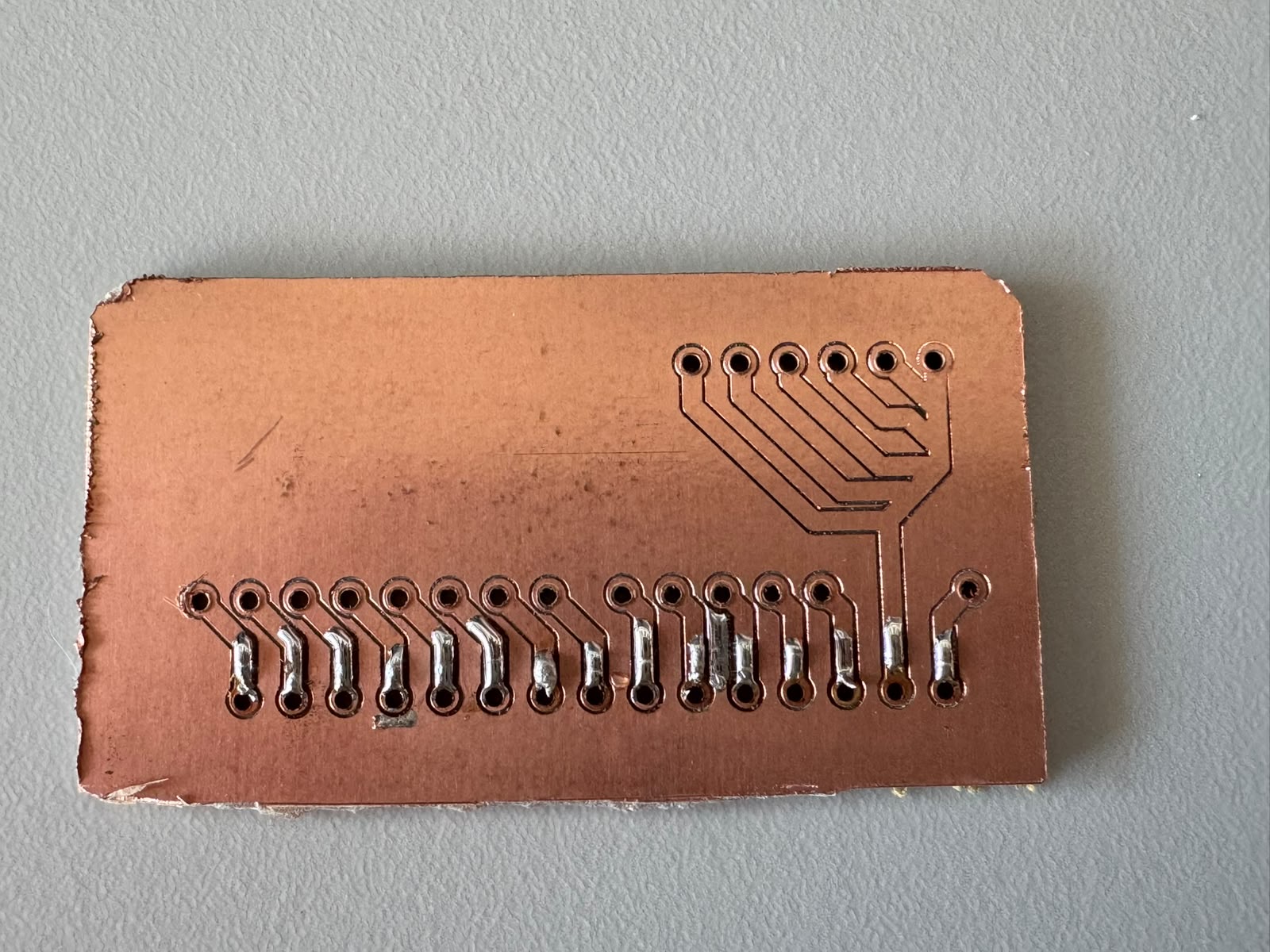
So I started creating my own files. Starting by editing an existing footprint to match my size, position and needs:
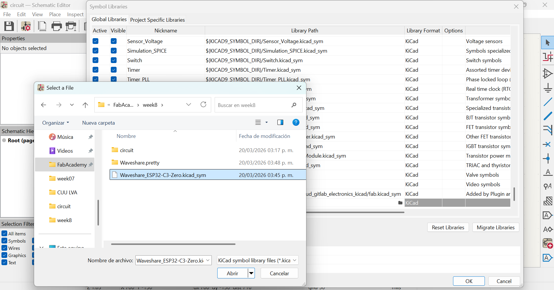
Then I also created my own schematic from a similar one, making sure all pins where named and configured correctly:
Then I got a simple Code ready with Arduino IDE, not knowing I would be having trouble uploading it to the board.

The first mistake was using the wrong cable (only charging, no data) and not choosing the right COM.
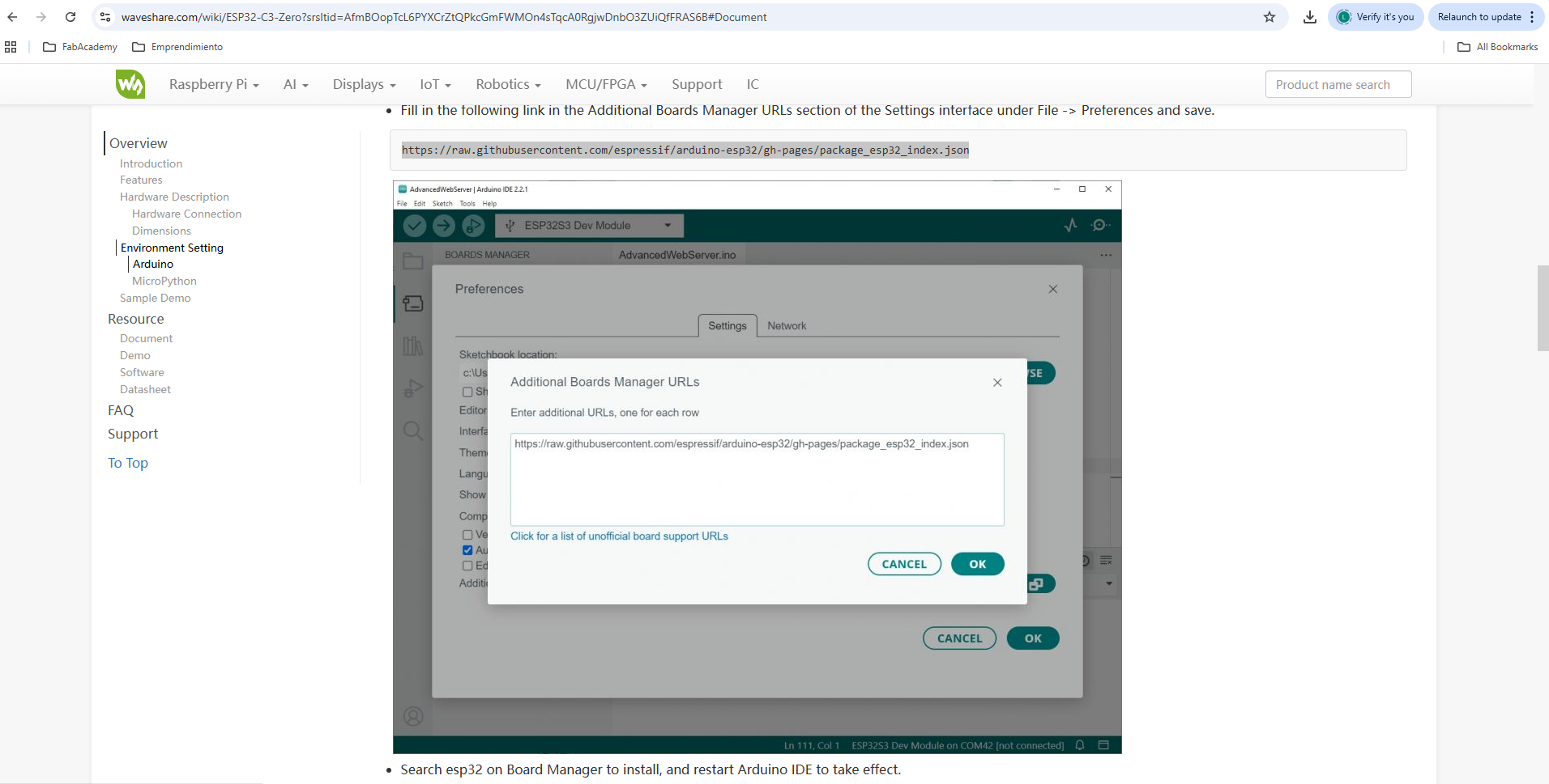
After that, I went back to read the documentation and noticed an additional board manager had to be manually installed, so I did that:
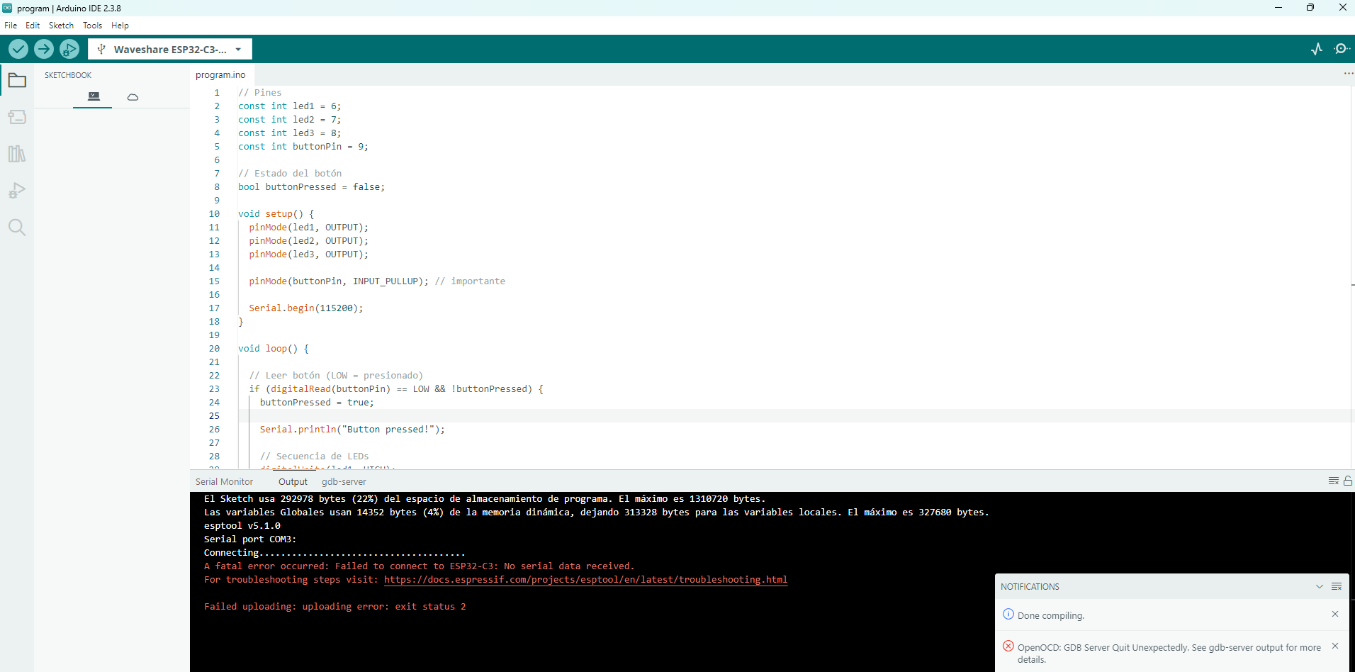
With that, I was finally able to upload the code.
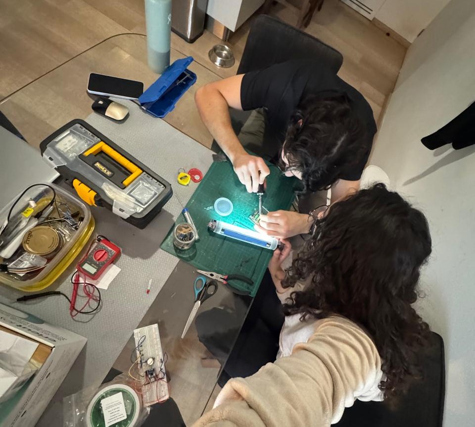
Then I came back to the physical world to try out all components and connections:
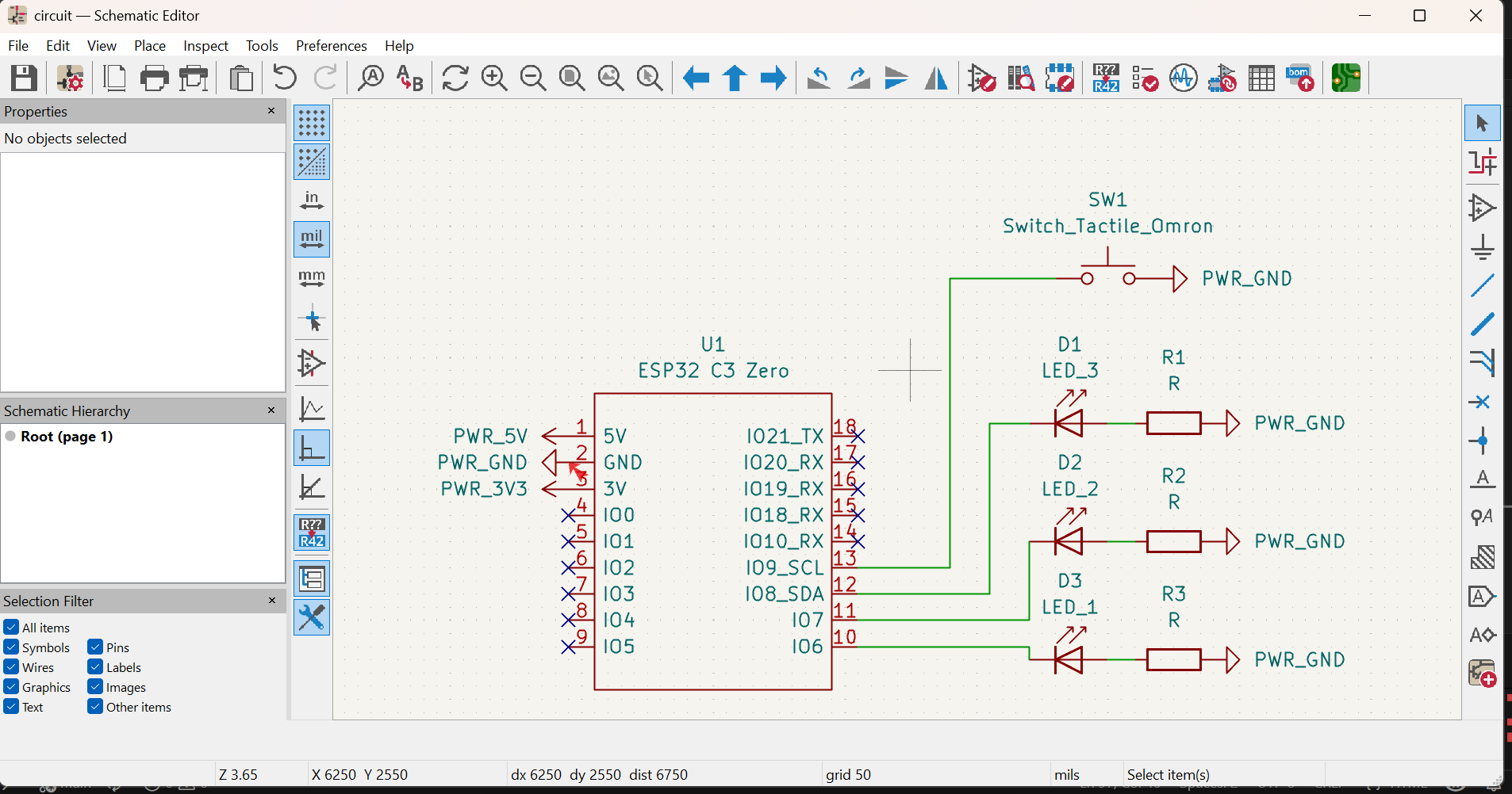
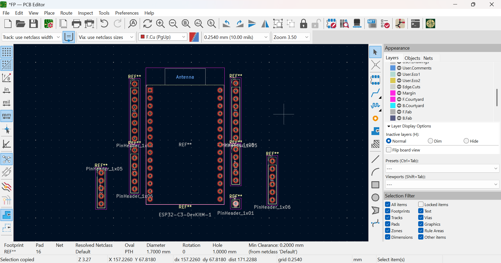
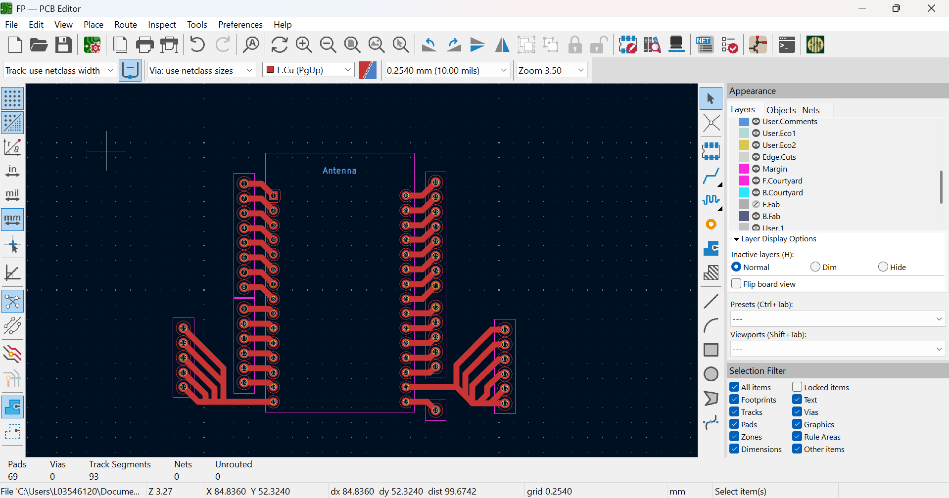
After that, I finally got to design the full schematic of the circuit. Adding my LEDs, resistors, a button and connecting evrything together:
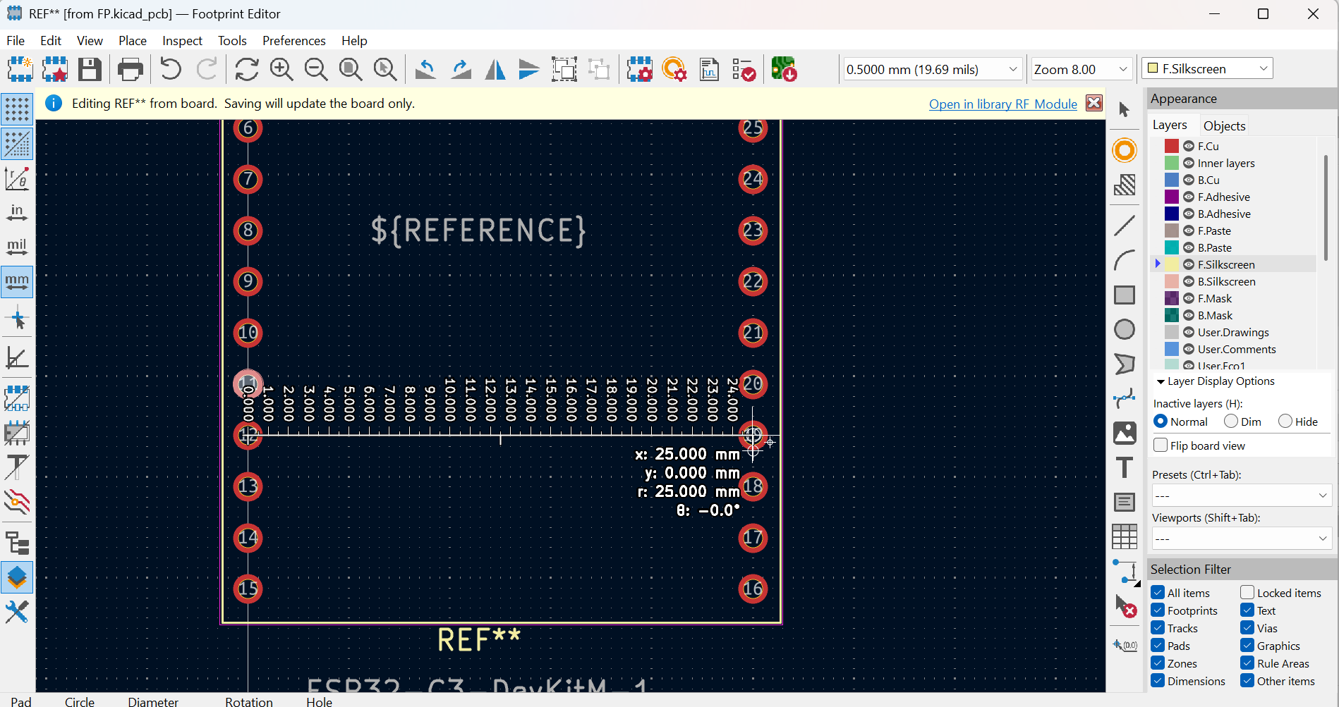
The next step was to design the PCB footprint from the schematic. But when I imported the components, I noticed the resistors qhere missing, so I tried adding them manually:
But then, when I tried connecting the components, I wasn't able to connect some together:
I looked for the reason and it turns out that the resistors I was using did not have a footprint assigned and you can't just add components manually because the have to be referenced in the schematic, creating a single net. So I assigned the footprints that matched my components in the schematic and then the connections appeared as they chould:
I also learned that the pin numbers in the footprint need to have the same names as the ones in the schematic, so I went ahead and corrected that:
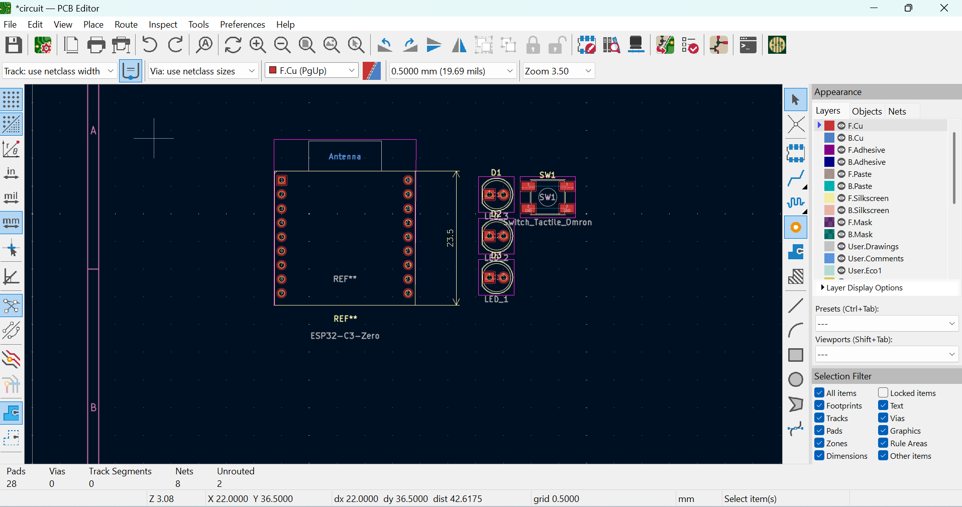
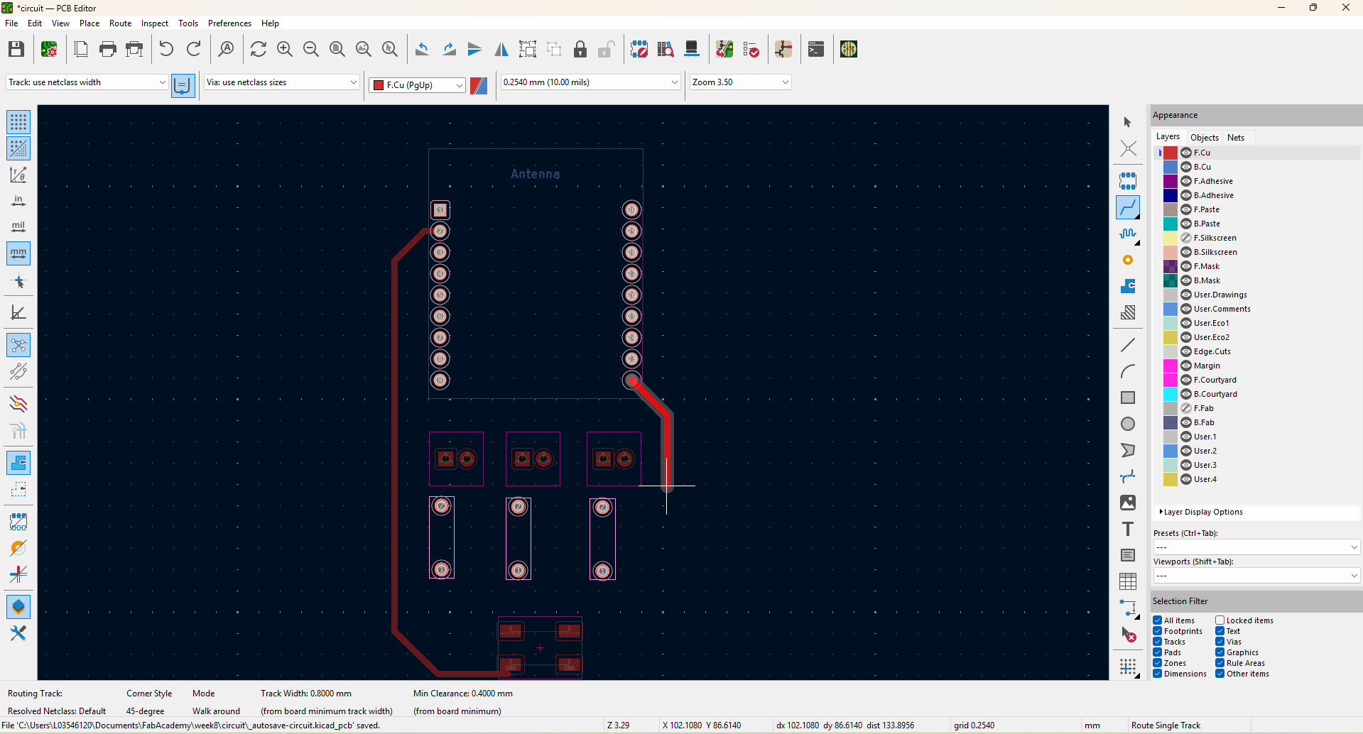
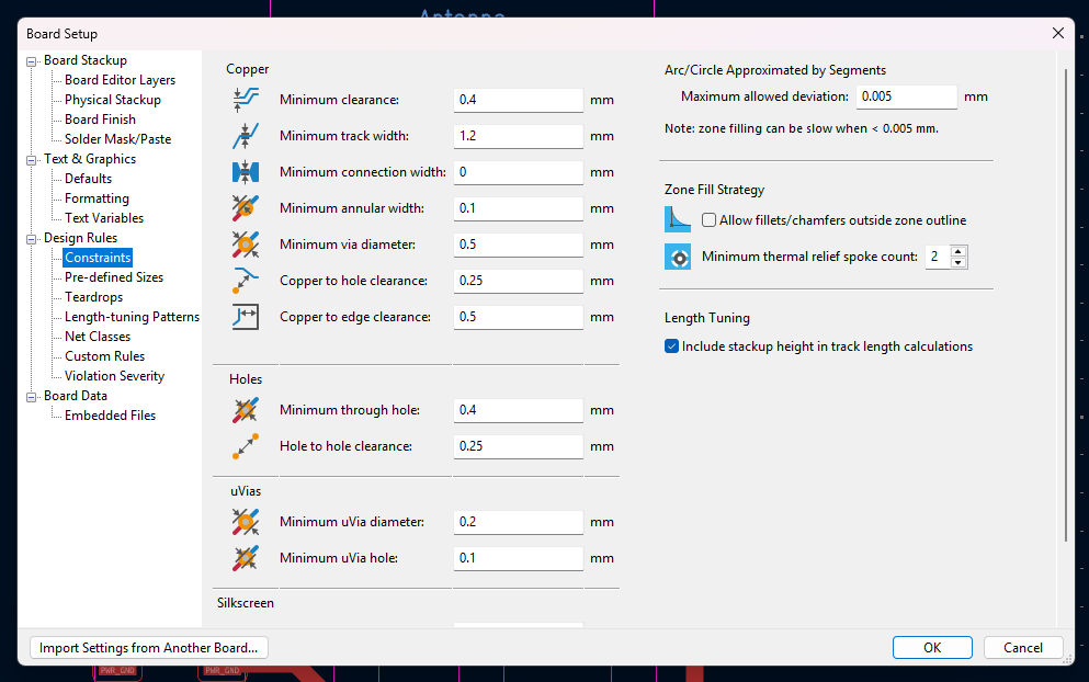
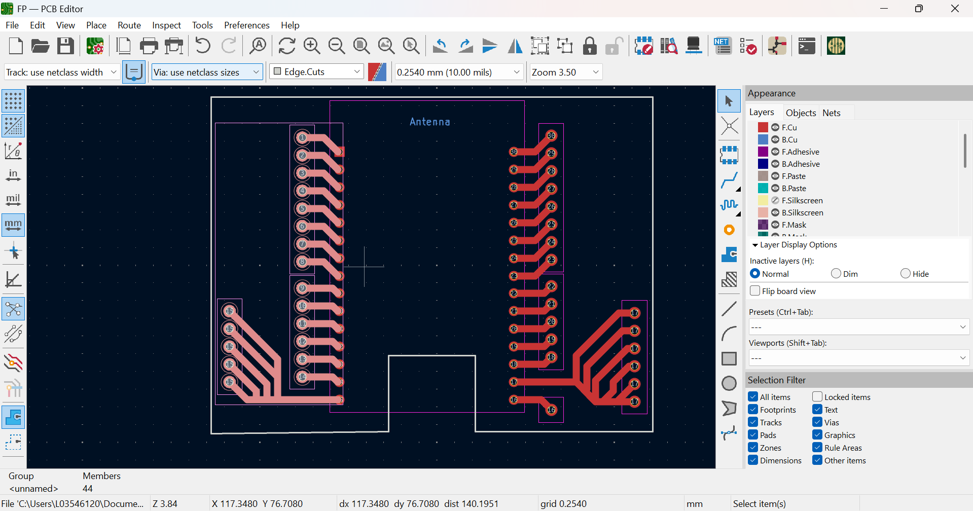
The SetUp for the tracks I used was the following:
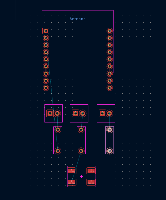
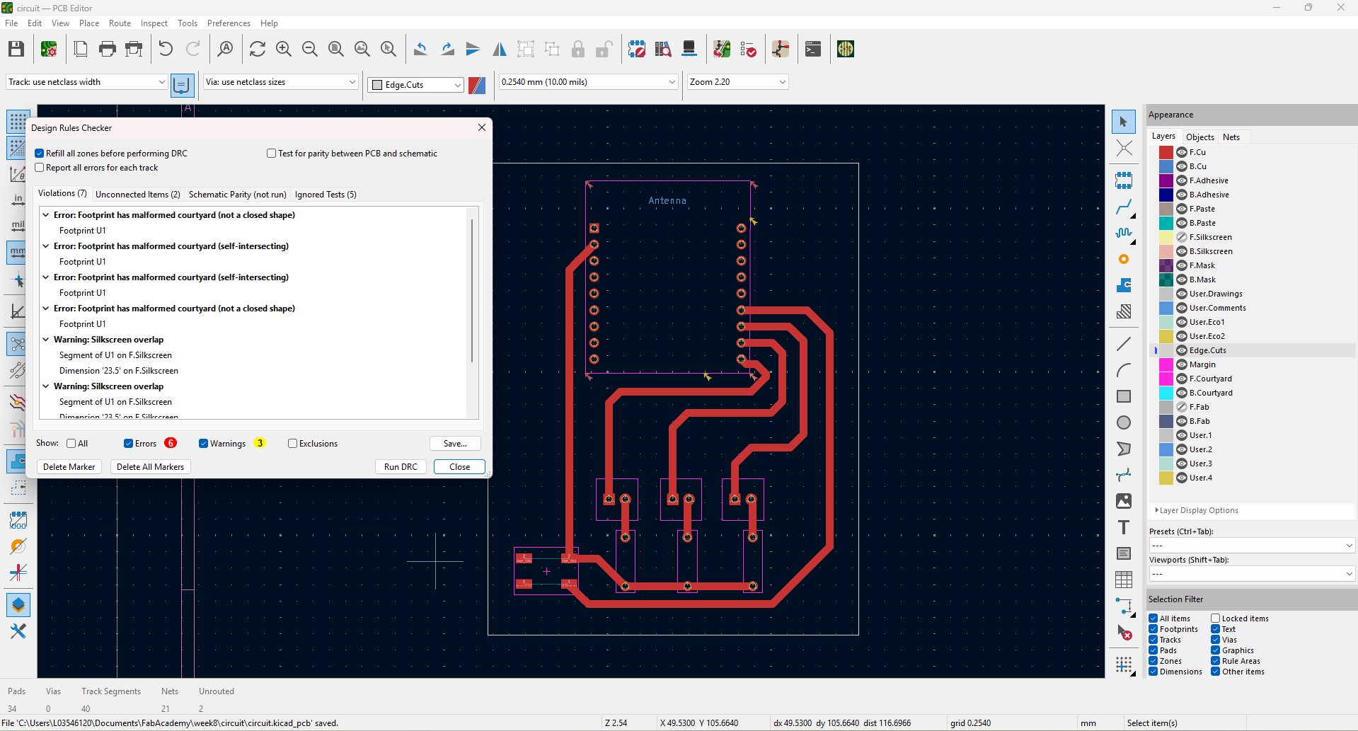
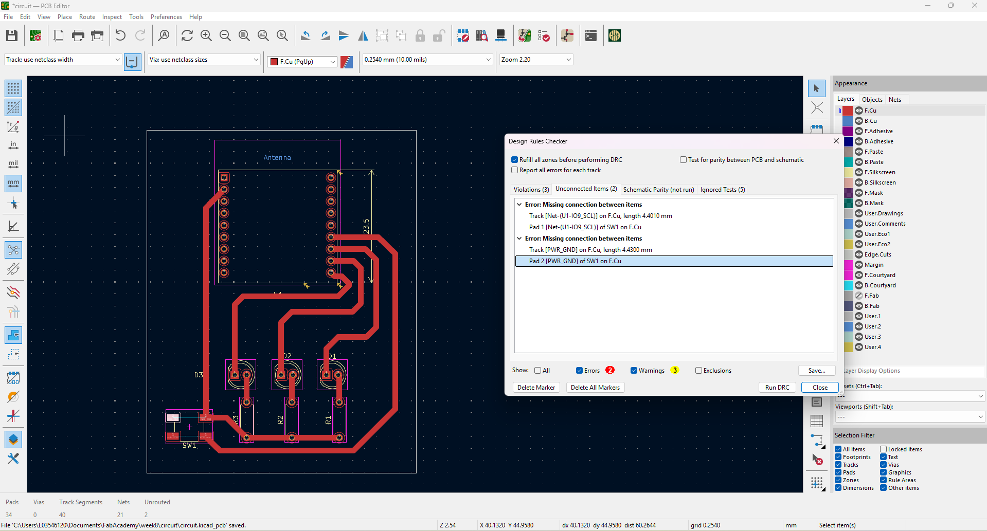
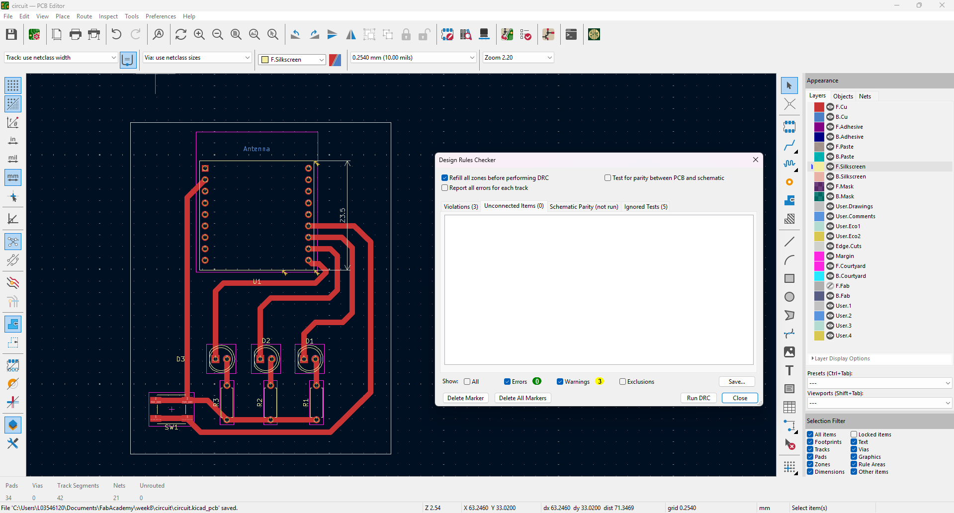
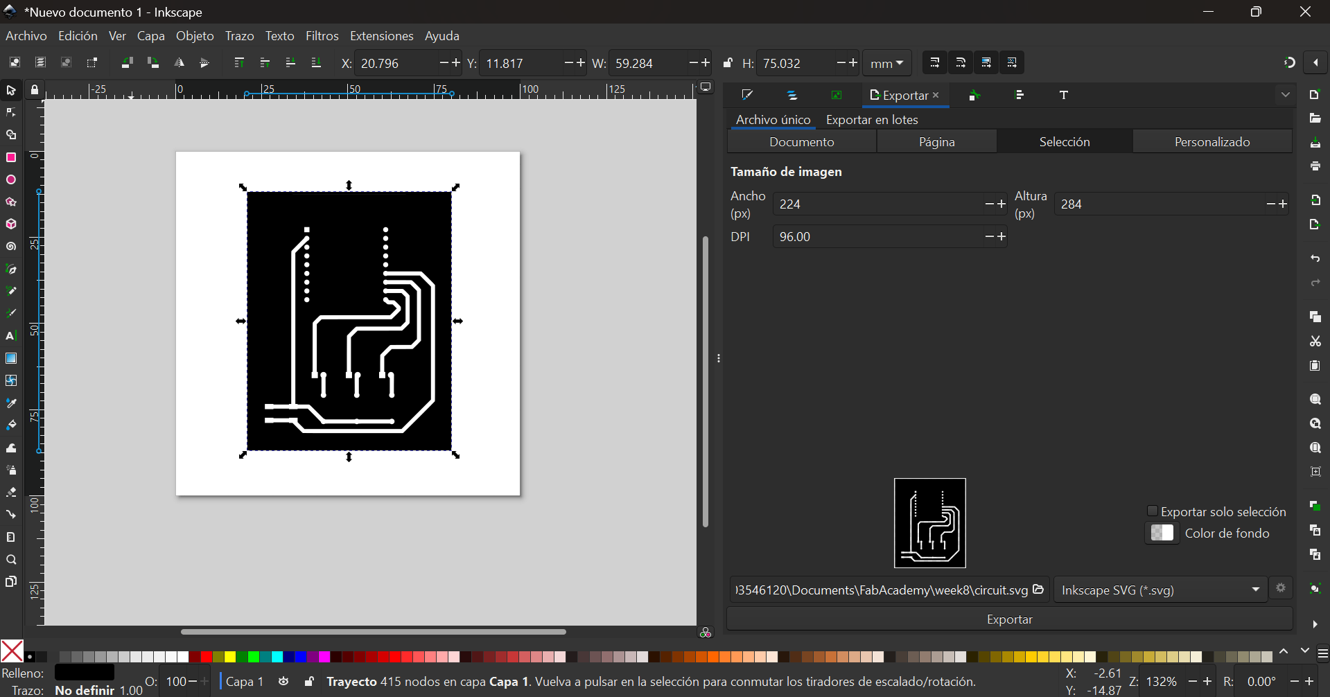
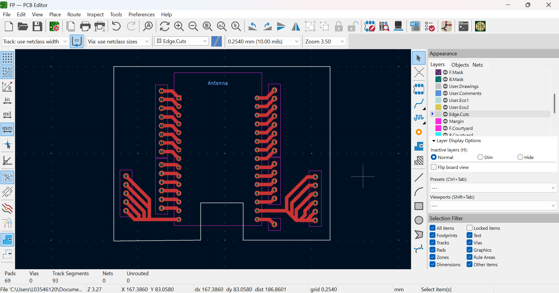
And for the final KiCad step I did some rulechecks, had to delete some little lines and ended up with my final design:
Working PCB
Getting to this point had already been a ride, but it doesn't end here. Making a working PCB with the materials I had toos several iterations...
Here go the steps of my journey:
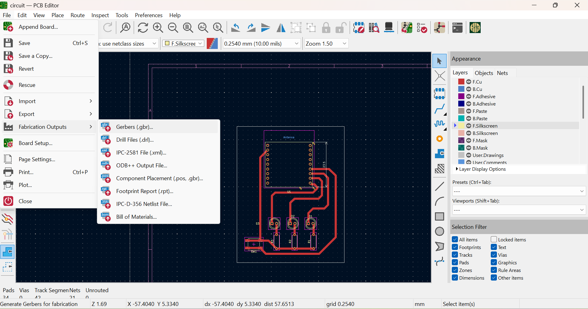
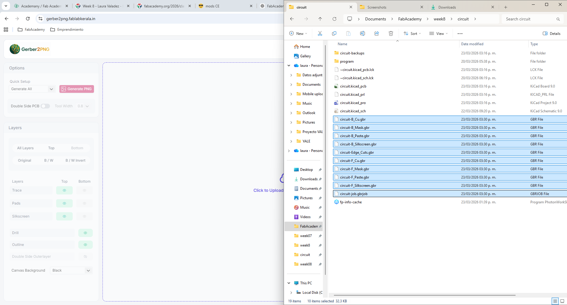
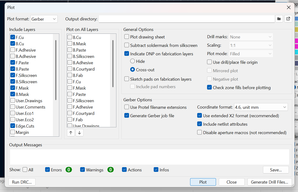
- Exporting gerber files from my KiCad footprints
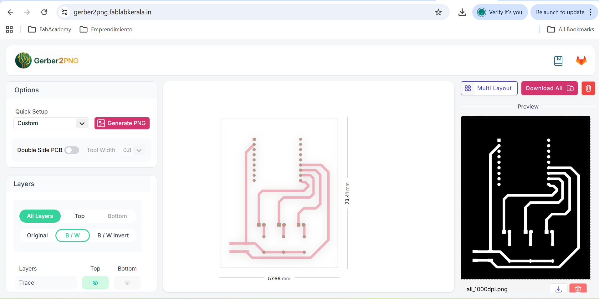
- Uploading the gerber files to https://gerber2png.fablabkerala.in/
- Downloading the png
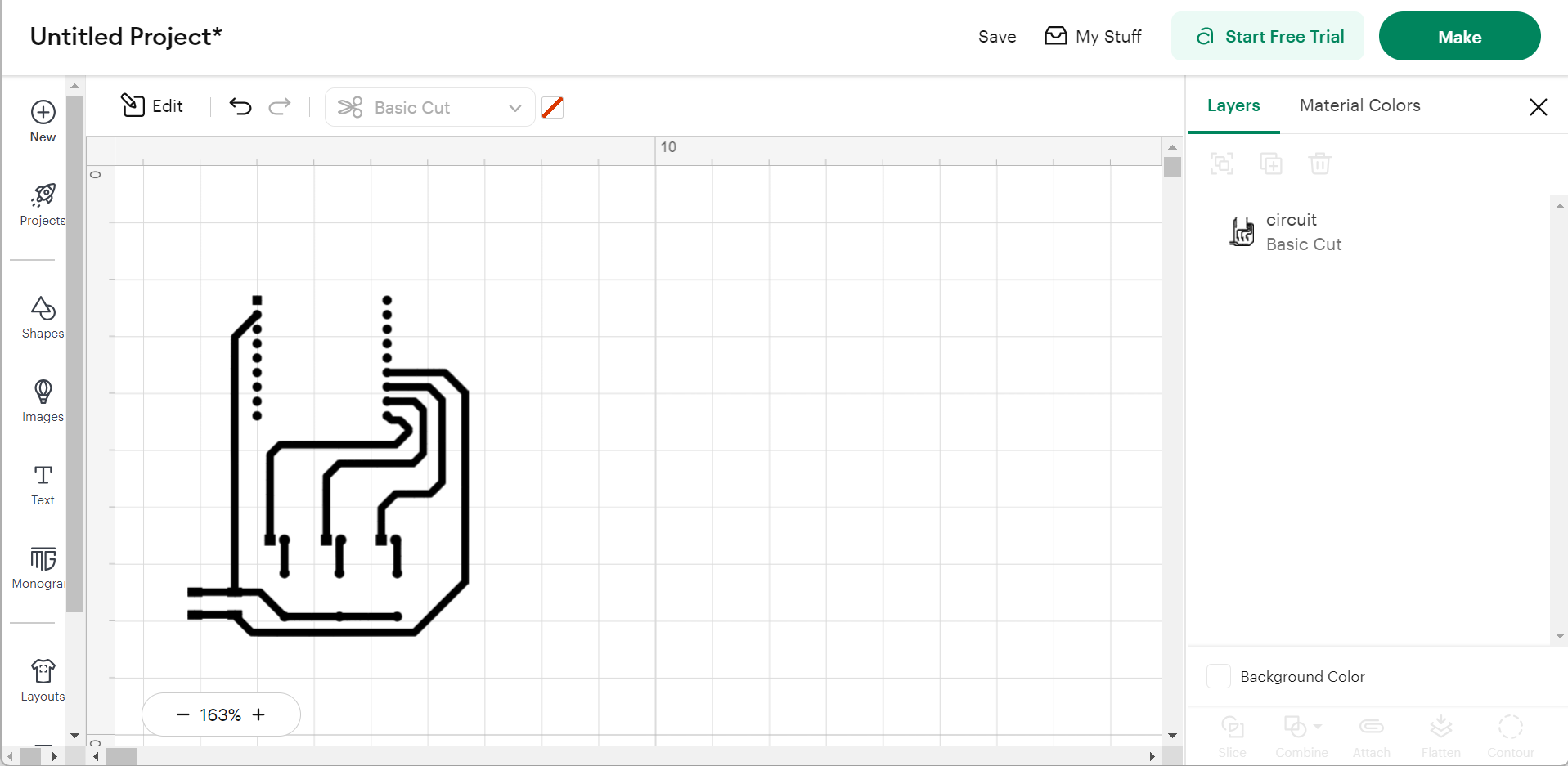
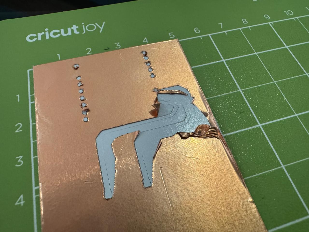
- Converting the image into vectors
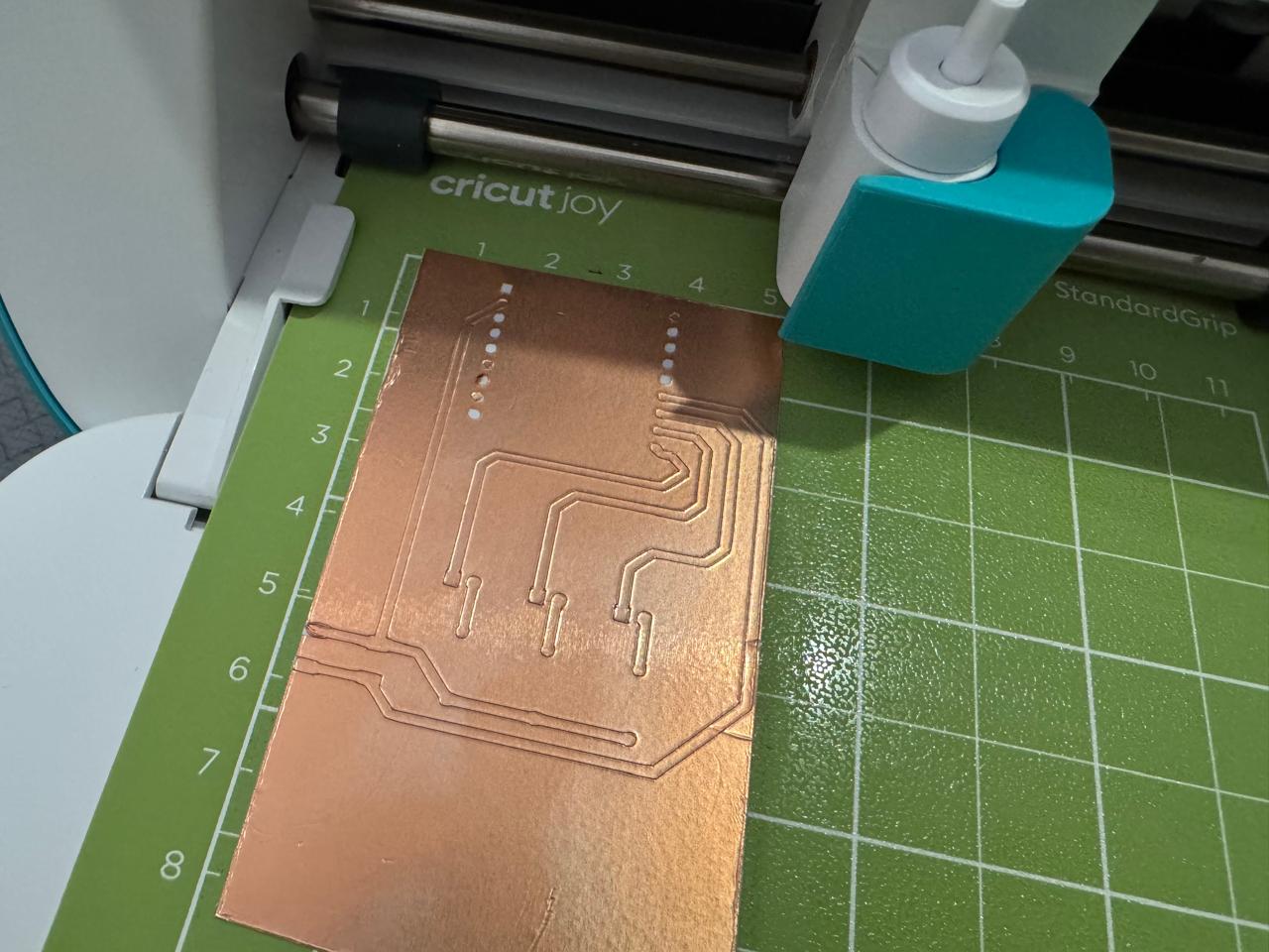
- Openning the vectors in cricut, making sure everything was the right size
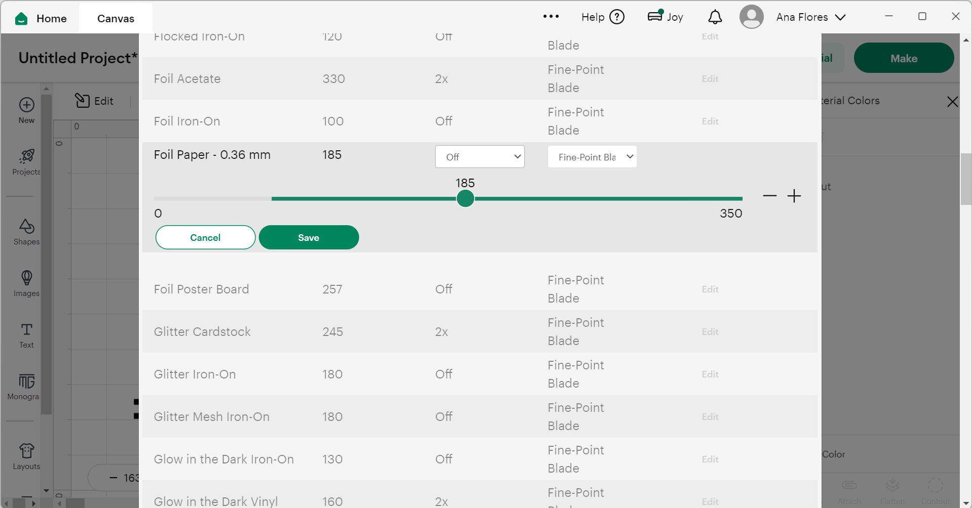
- Playing around with the cutting pressure to find the perfect match (turned out the lowest pressure possible was needed)
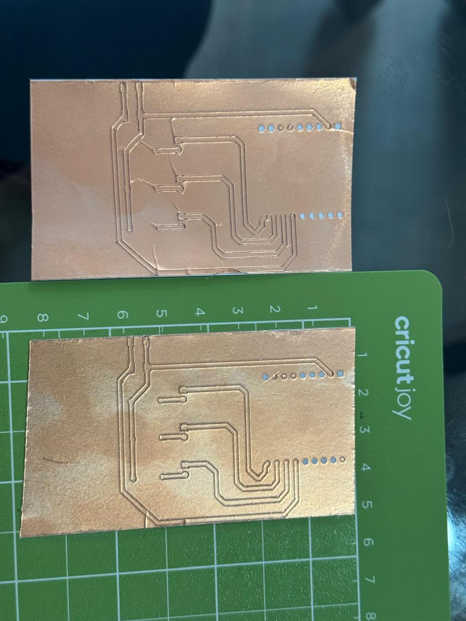
- Iterating with the different pressures until I got clean lines
- Made a back up just in case
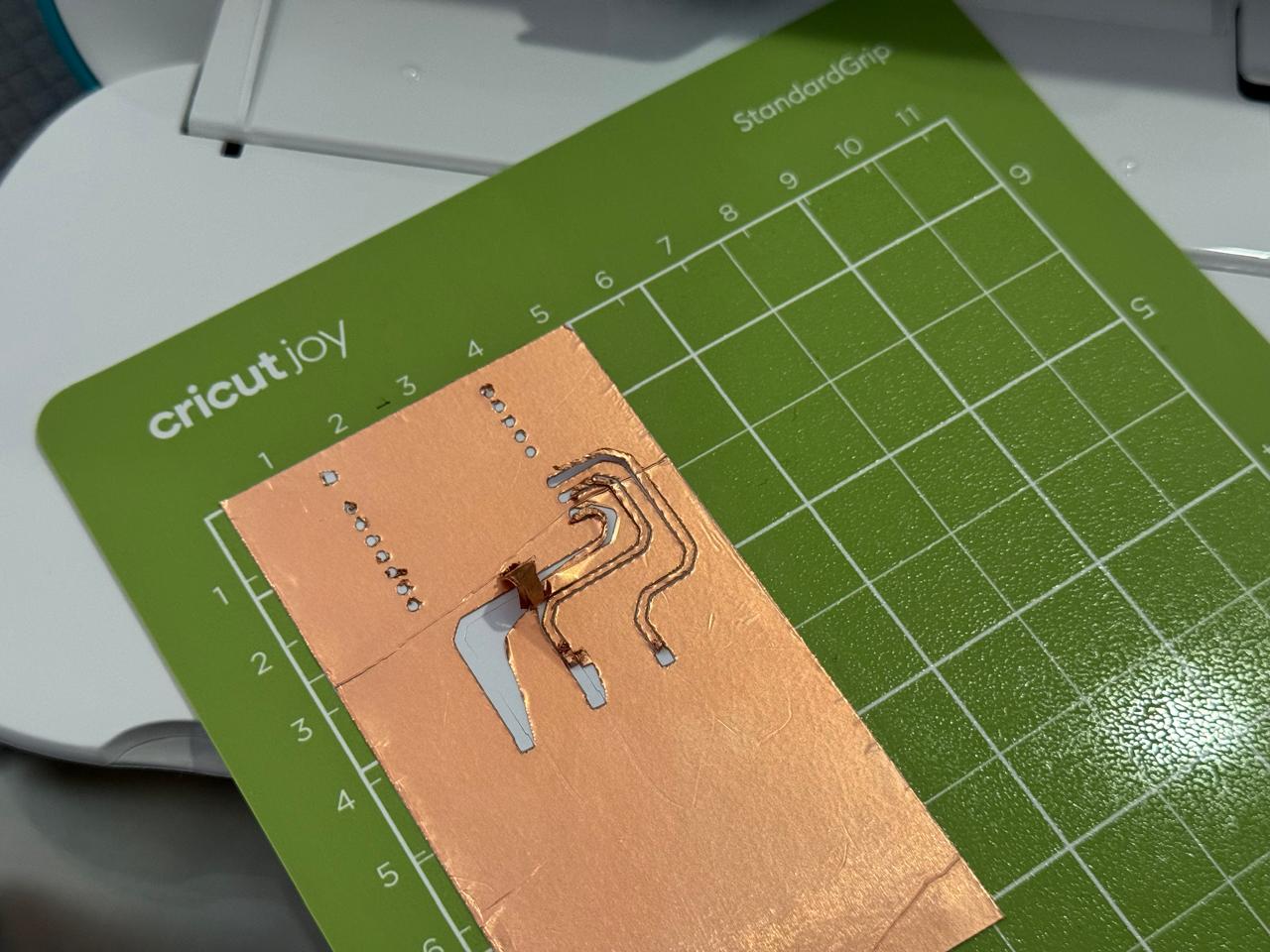
- Cleaning the cuts
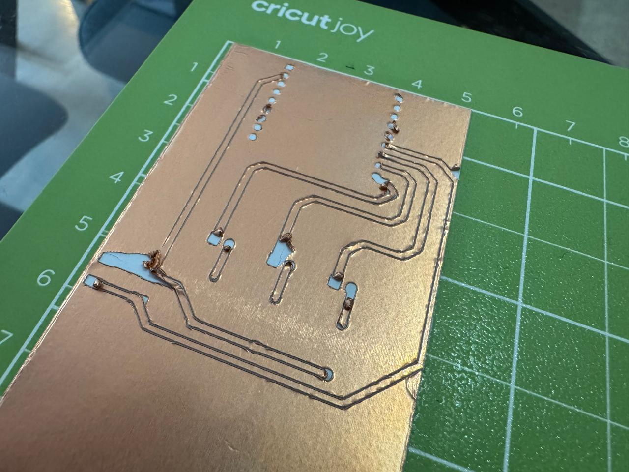
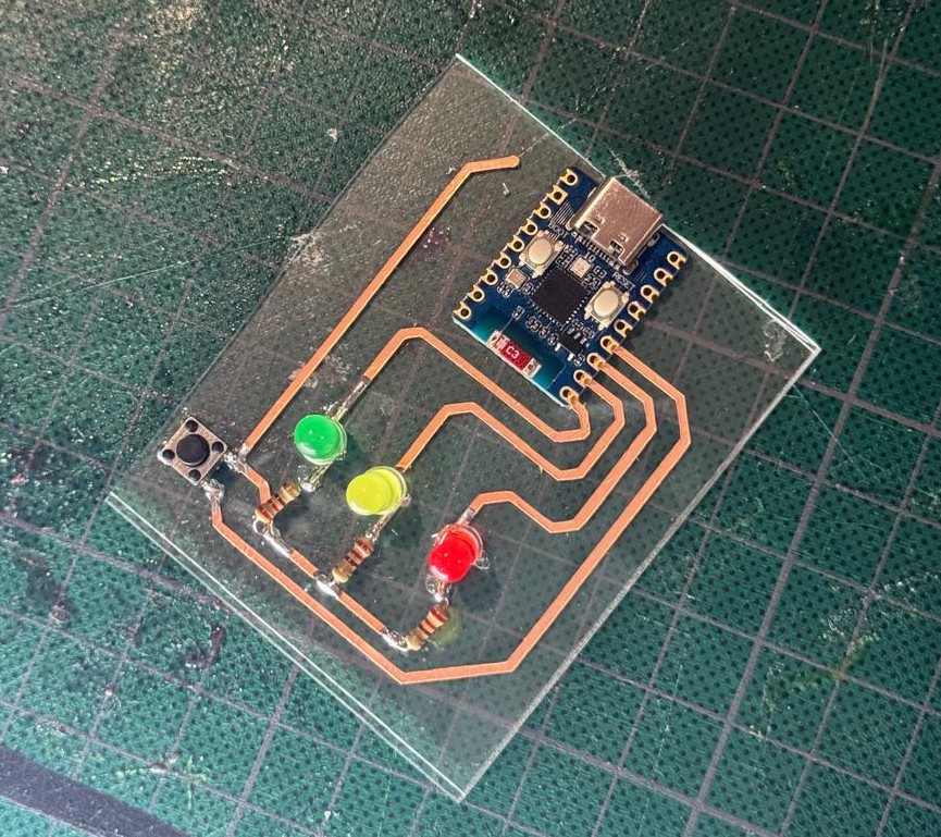
- Used transfer paper to get the circuit into an acrilic piece
- Soldered the components in place (with a little help)
- Finaly got the final PCB
- Testing the PCB

Final Project PCB Routing
To begin, I followed the same steps as before in KiCad to design my PCB. This time, using an ESP32 WROOM 32.
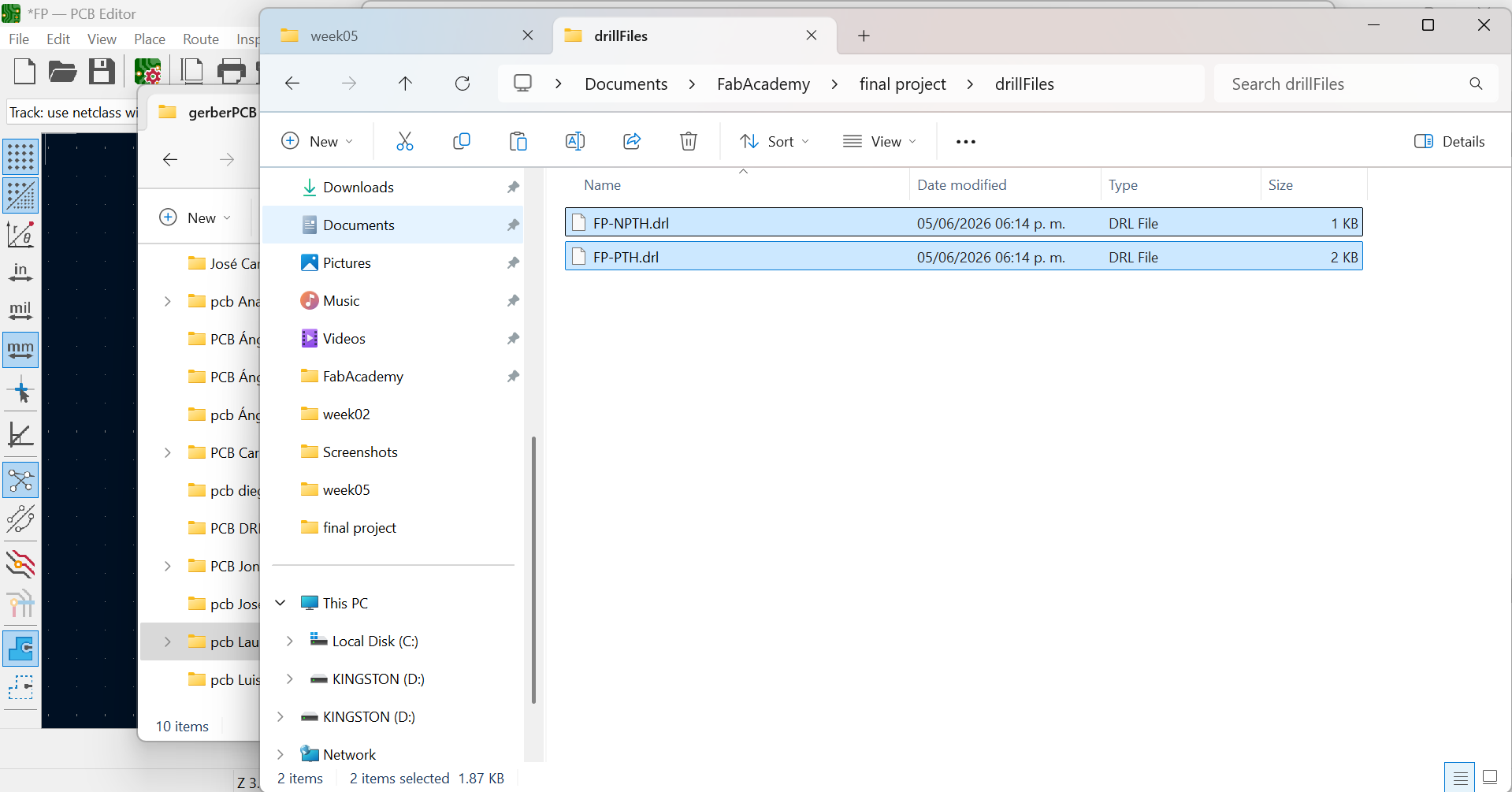
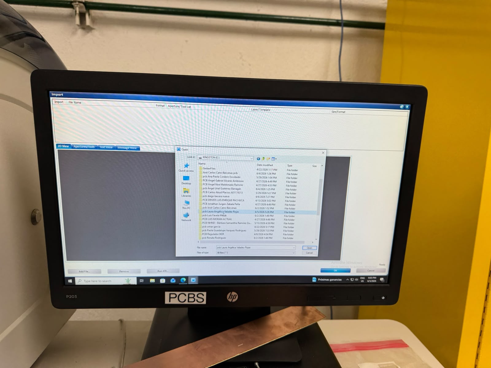
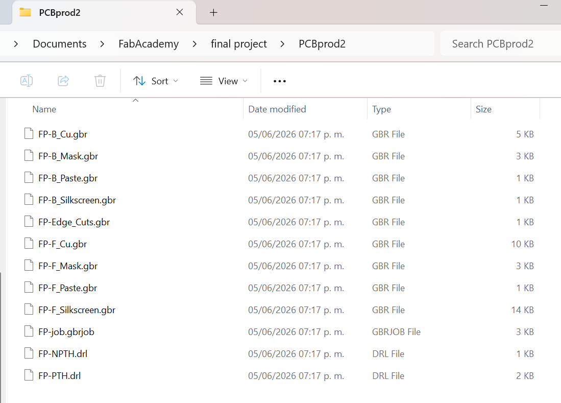
After some feedback, I insisted on using my campus' only PCB router to produce my final project PCB. I was able to get the permission by getting my gerber files ready, sending my request and contacting the lab manager. (Find all files below)

When I arived the files were ready in a USB, but we noticed drilling instructions where missing so I had to go back to KiCad and download them separately.
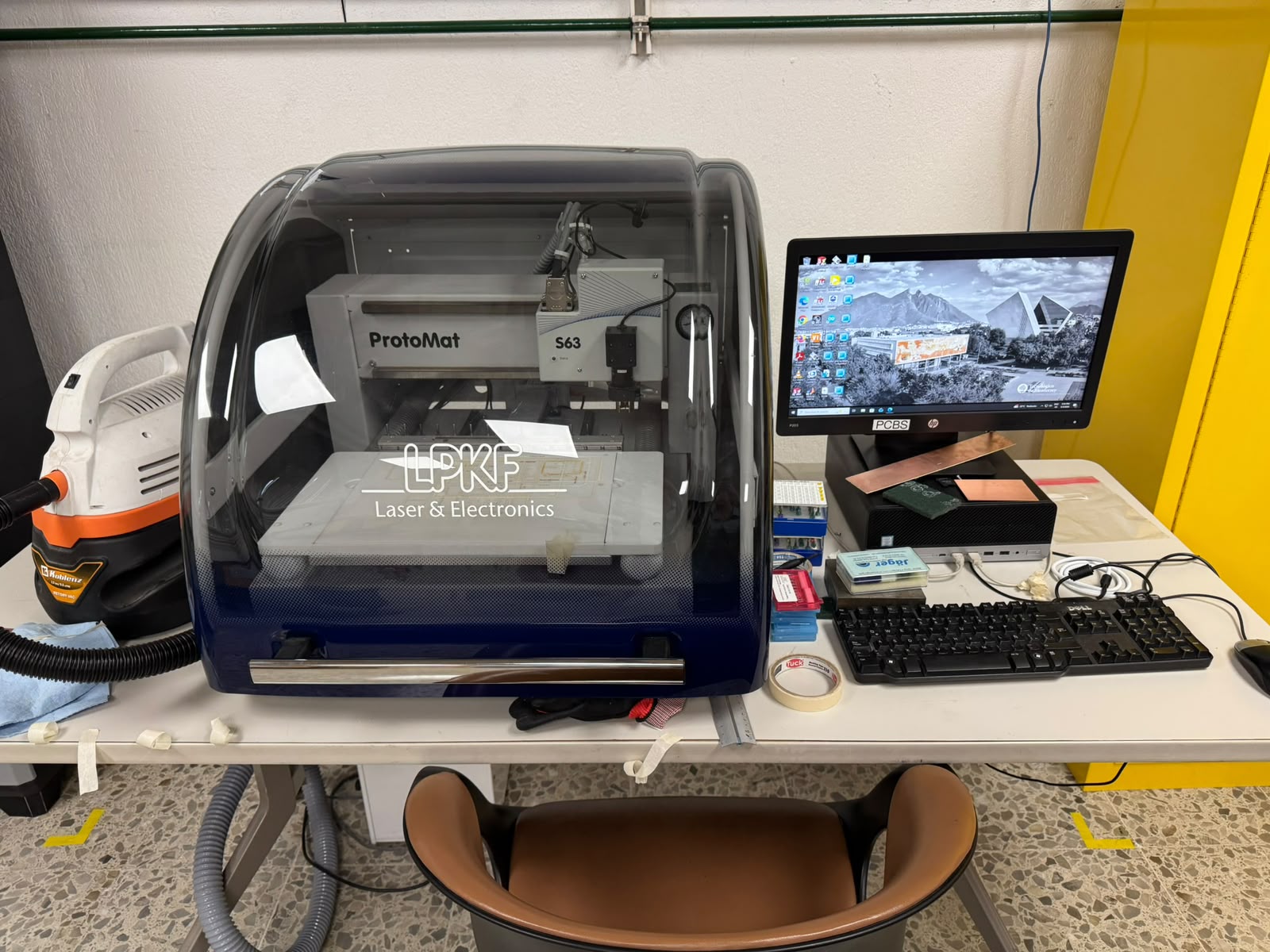
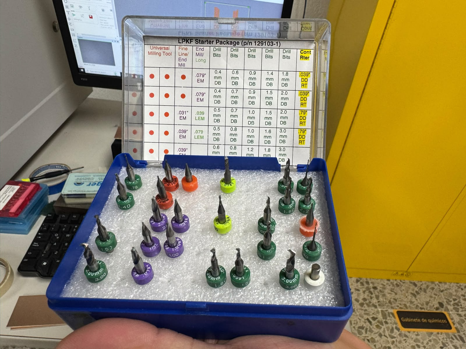
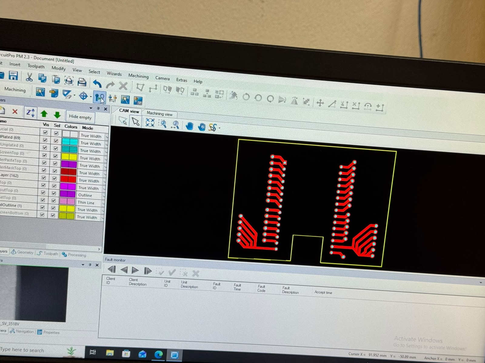
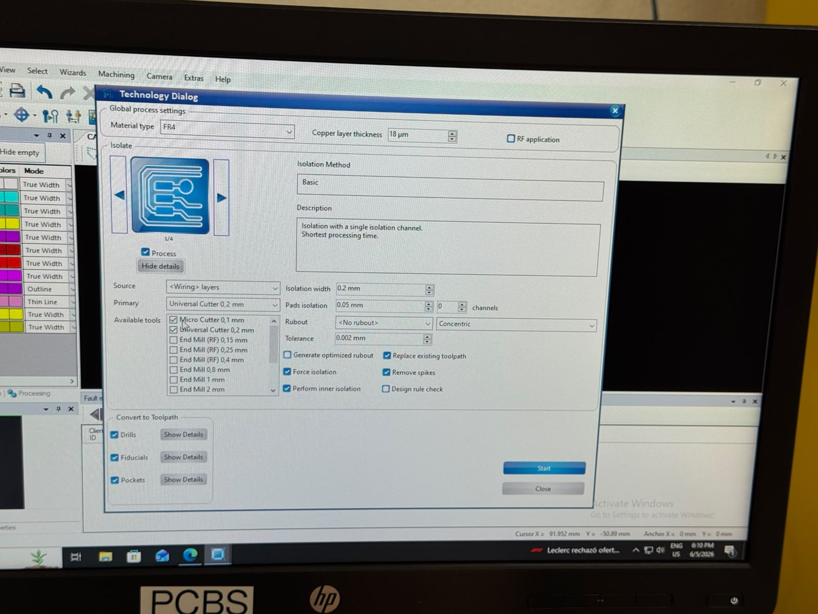
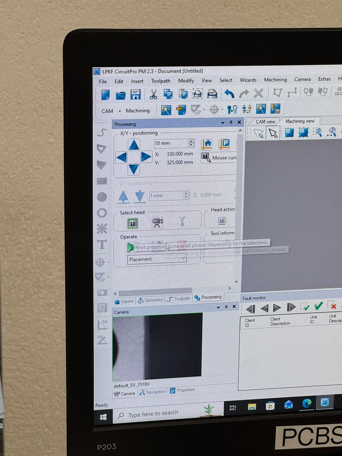
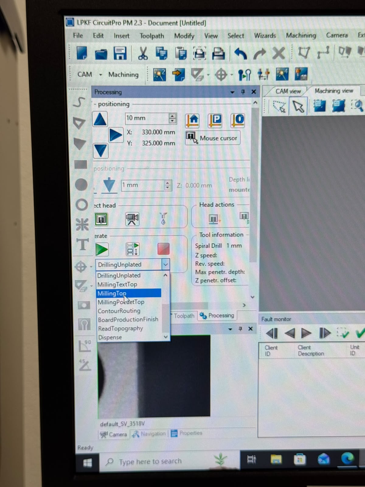
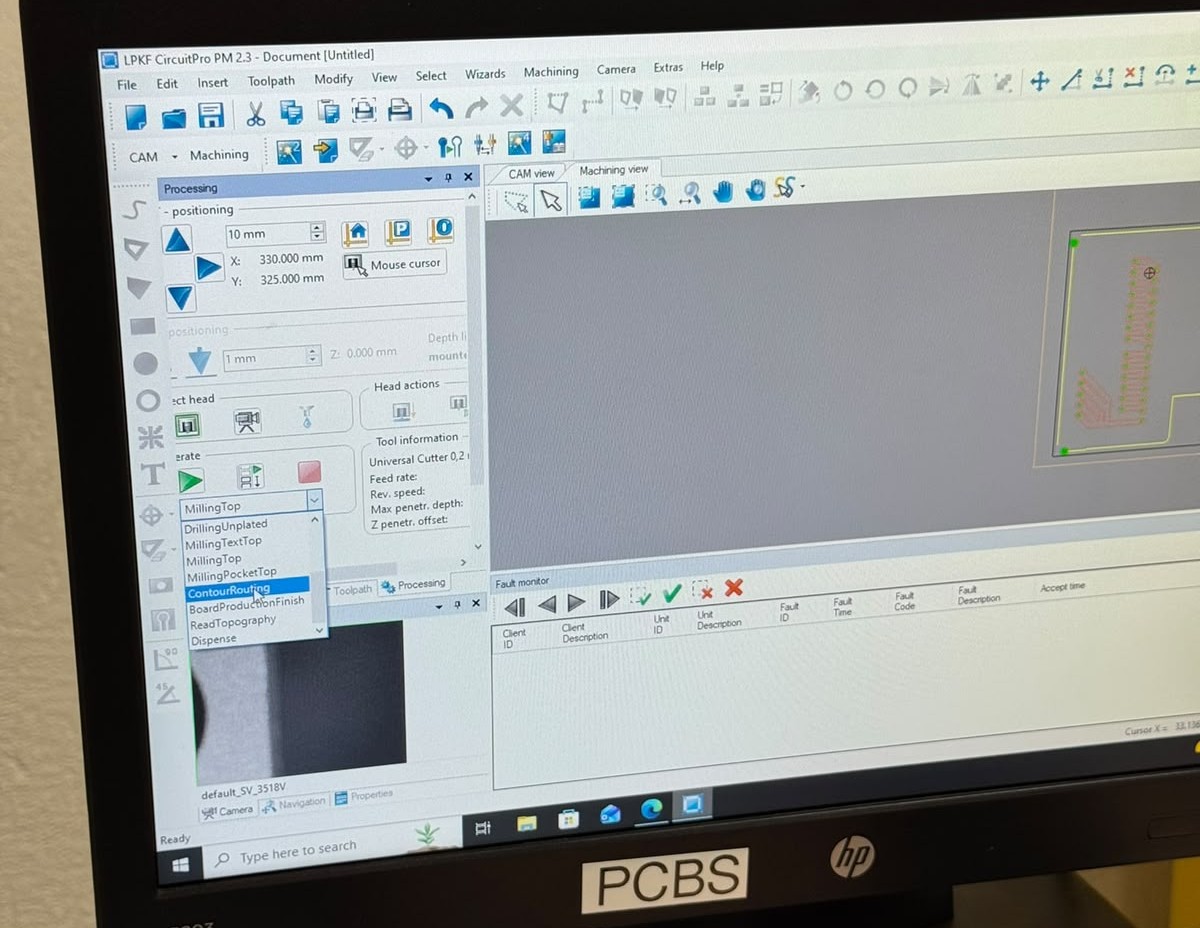
With that, we finally got to work on the machine: a LPKF Laser & Electronics ProtoMat S63, that runs with the software: LPKF CircuitPro PM 2.3. and uses several tools.
The first step was to turn on and connect the machine with the software:
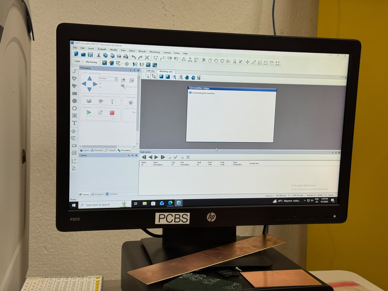
*This machine has a camera and sensors to set up automatically.
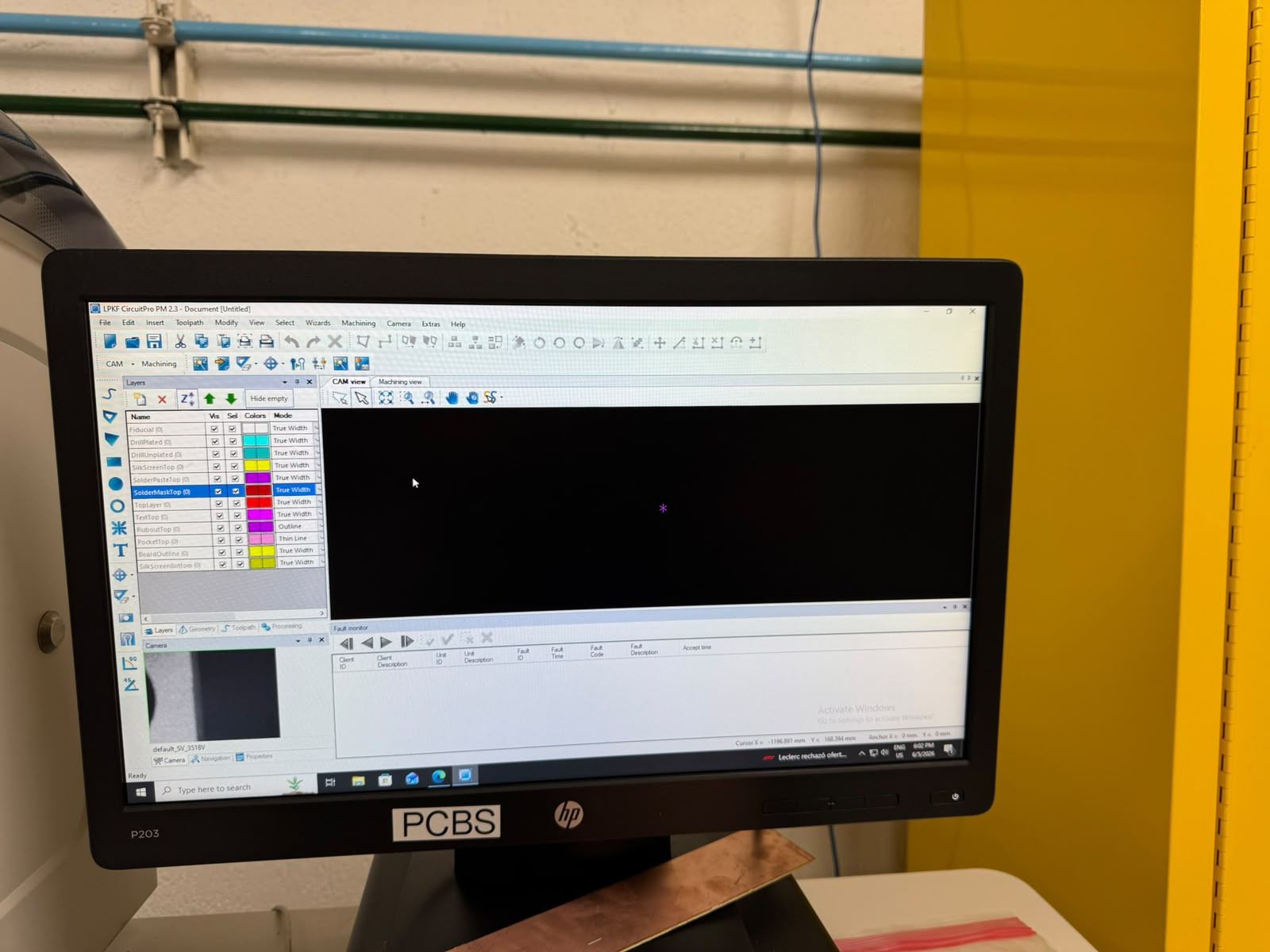
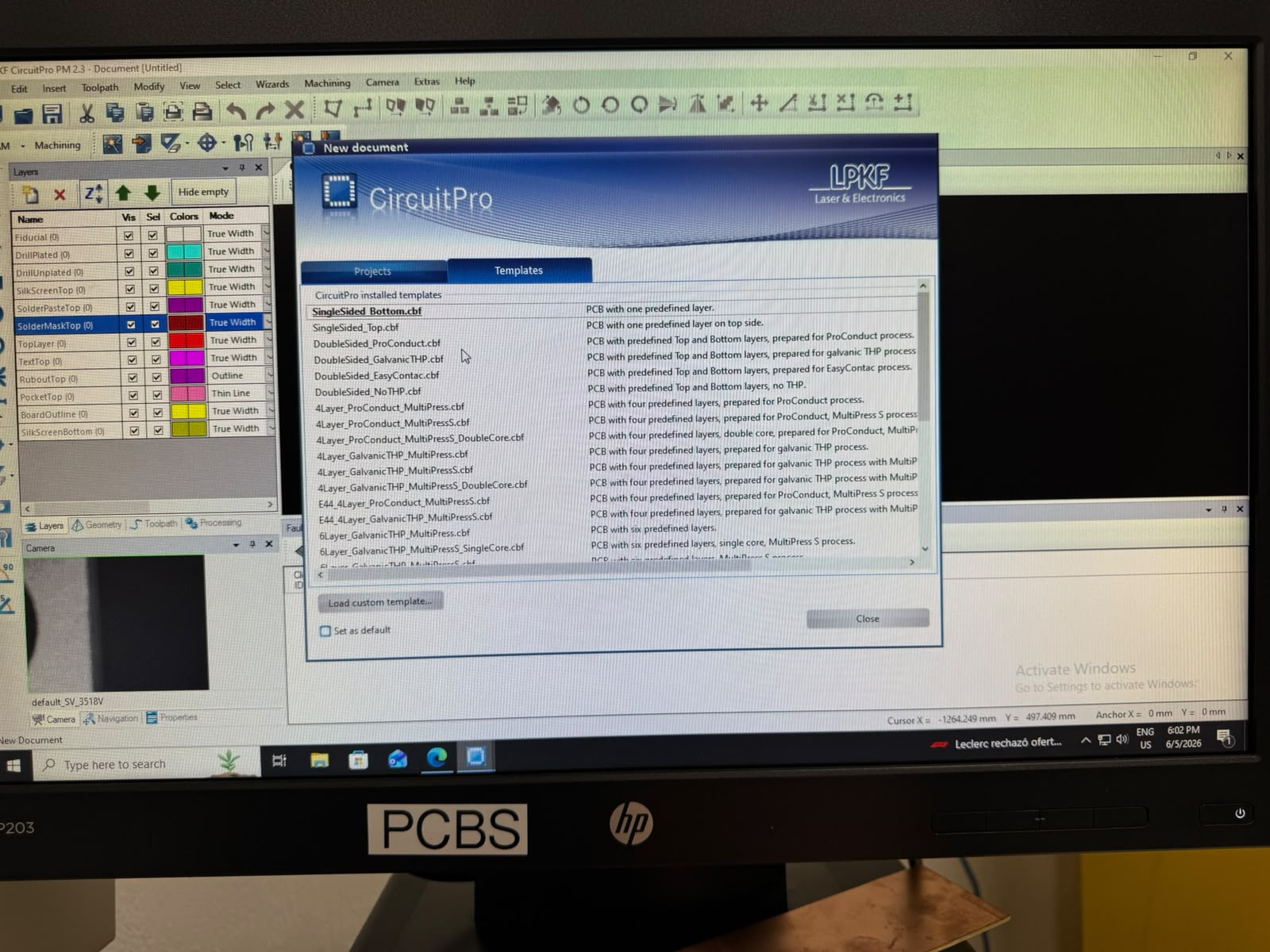
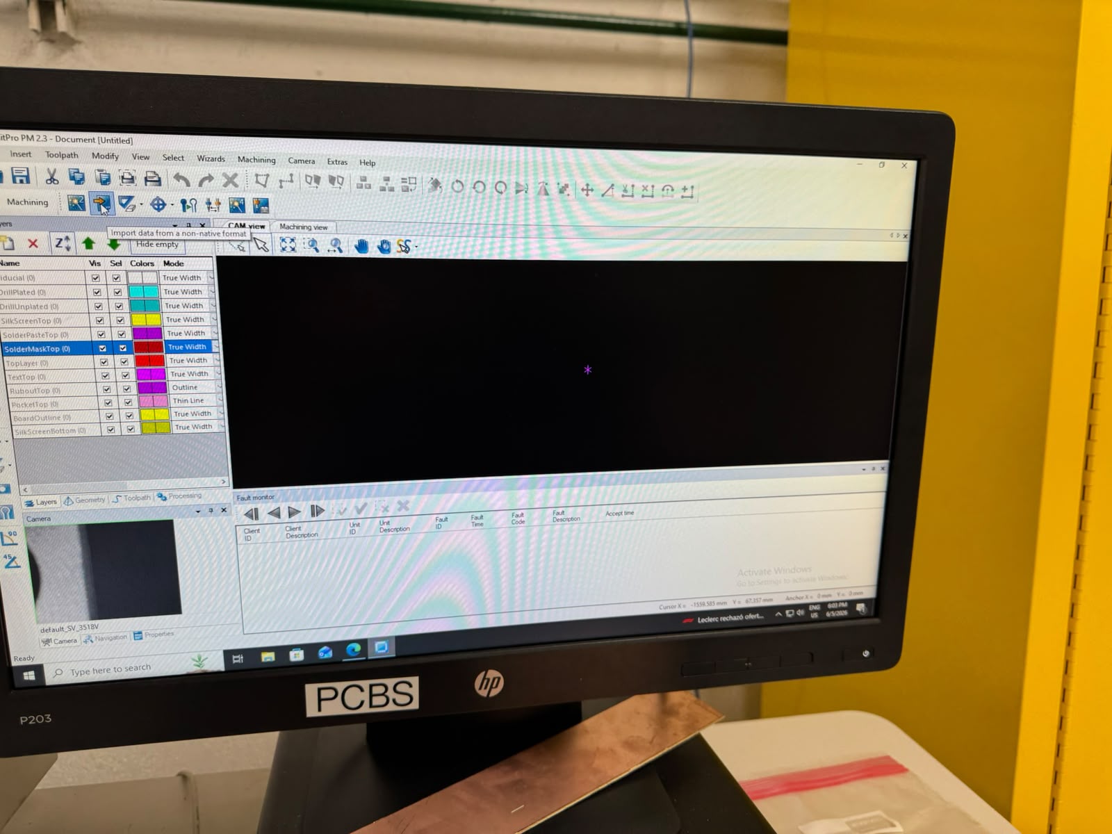
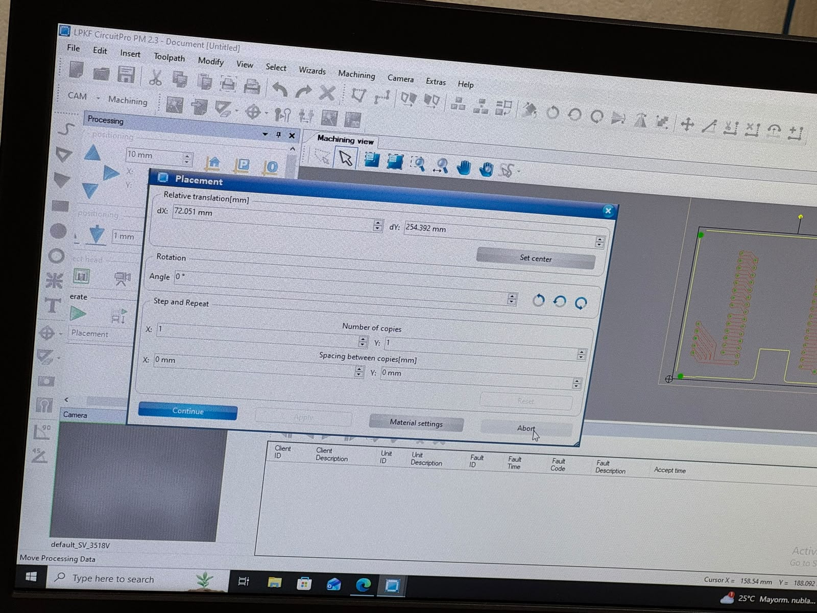
Once connected, we had to upload and select the layers of the gerber files we needed:
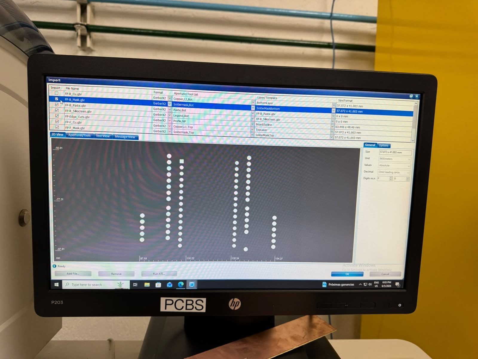
*We selected drills, outline rounting and paths layers.
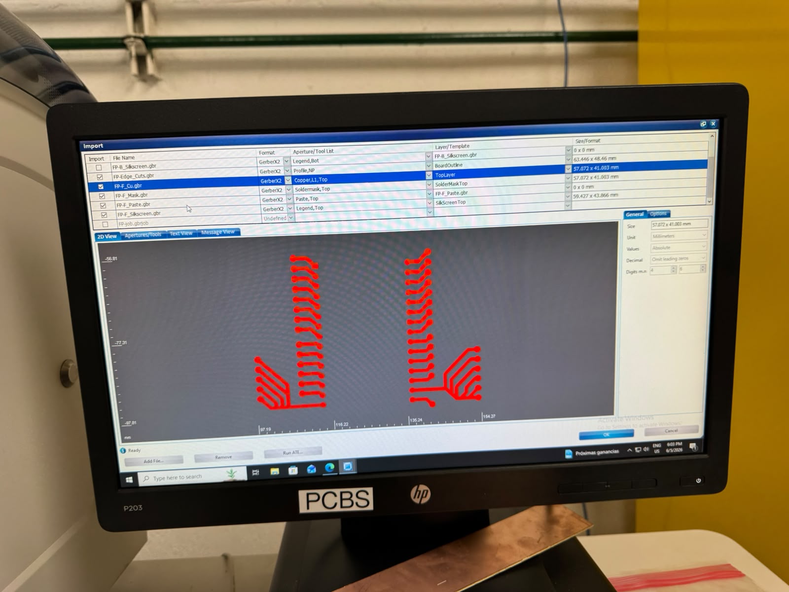
When we were able to see all layers, we checked the paths and tools assigned for the processes:
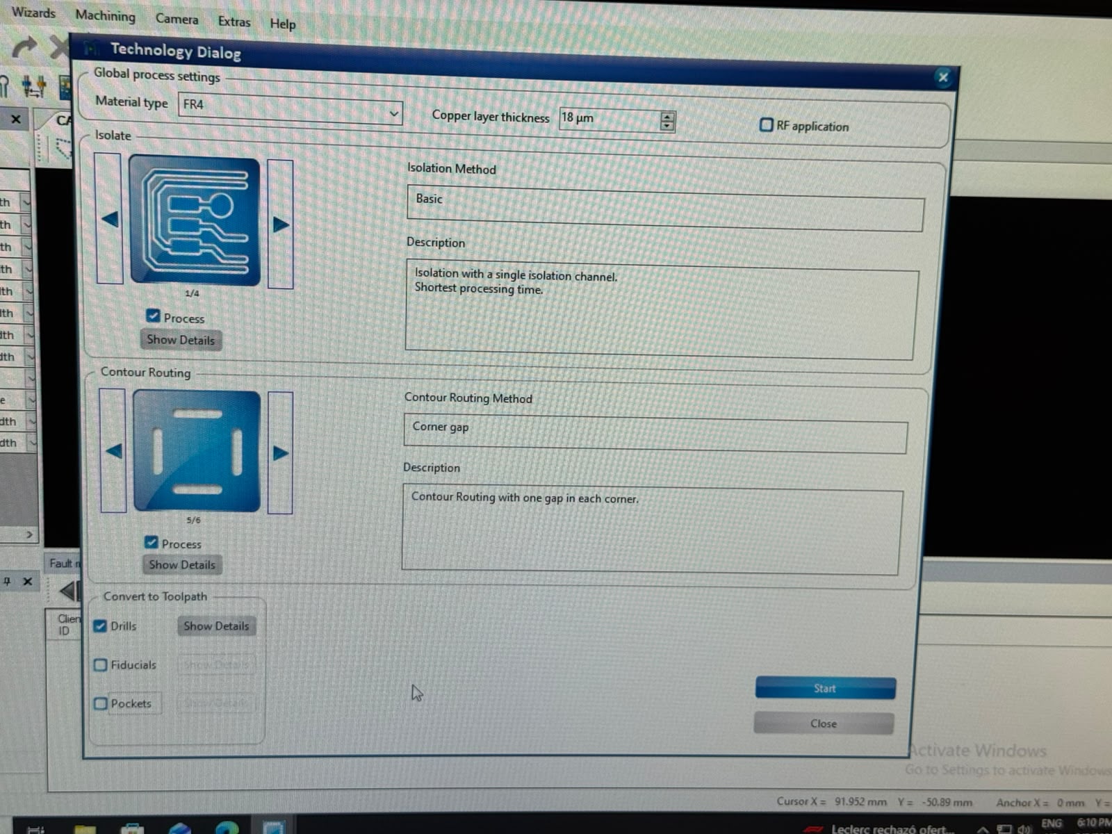
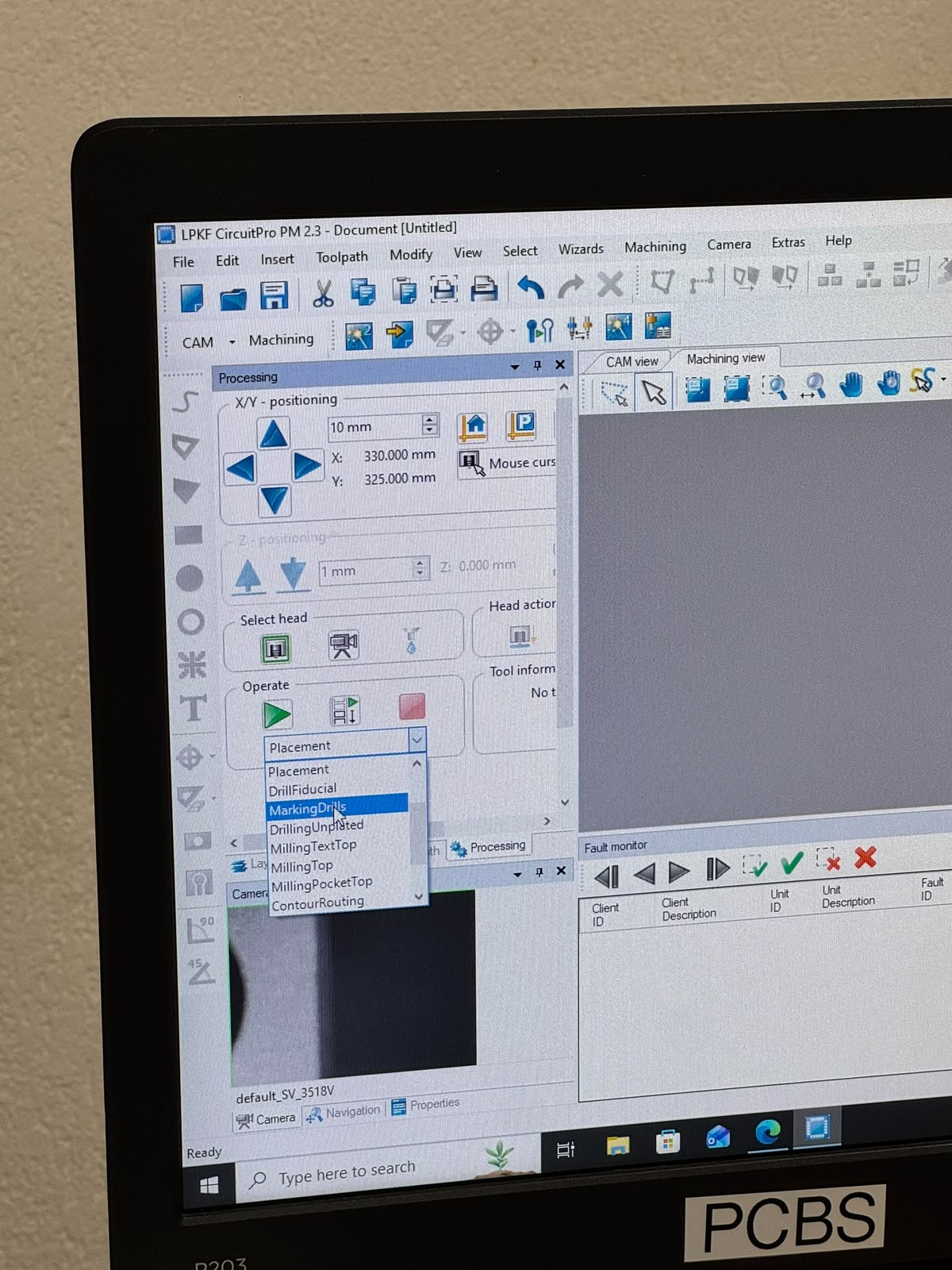
Then, we went ahead and followed the steps that the Production Wizard indicated:
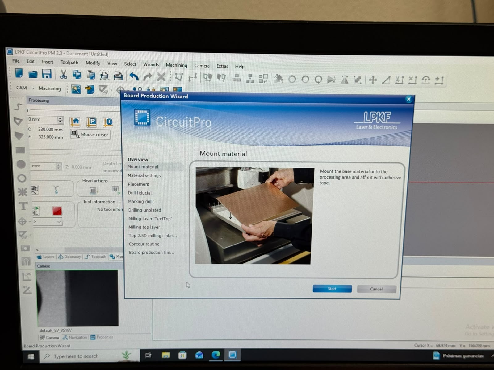
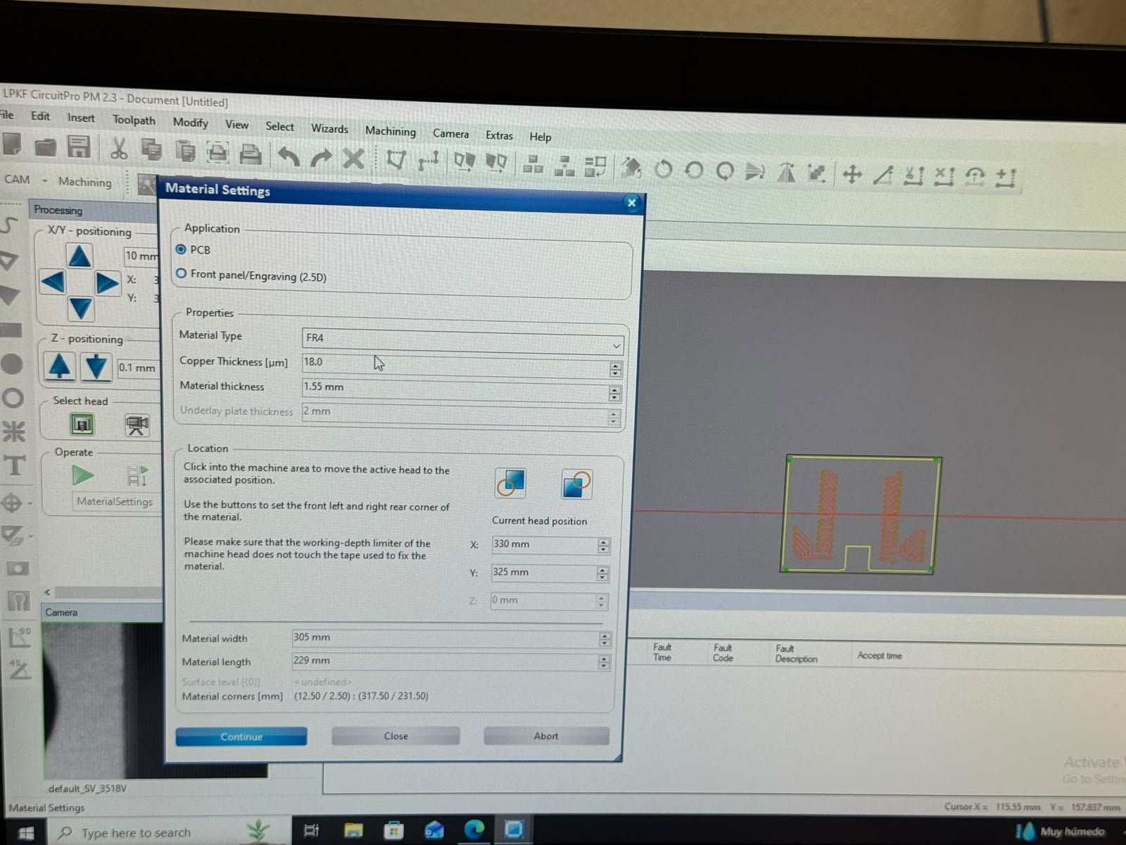
The first indication being to set up the material:
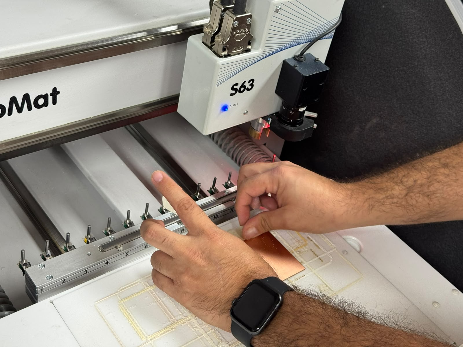
Then we had to indicate the materil's origin:
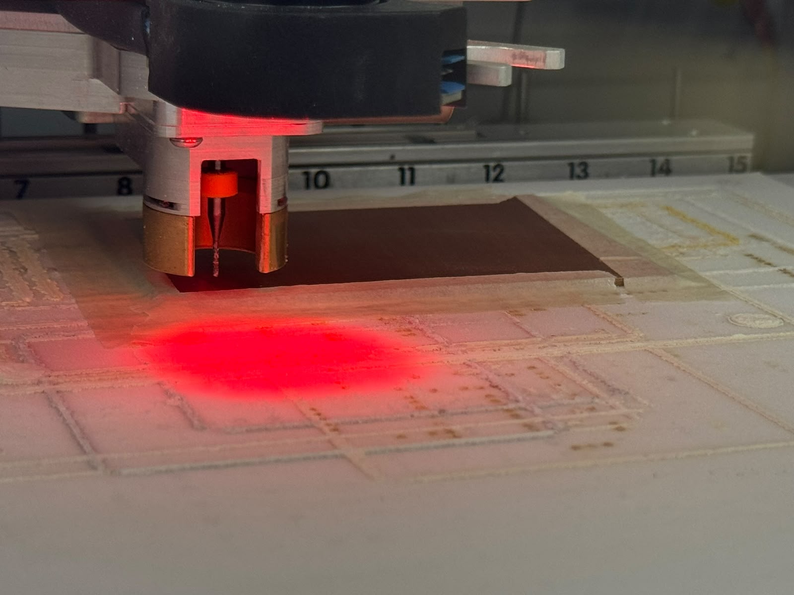
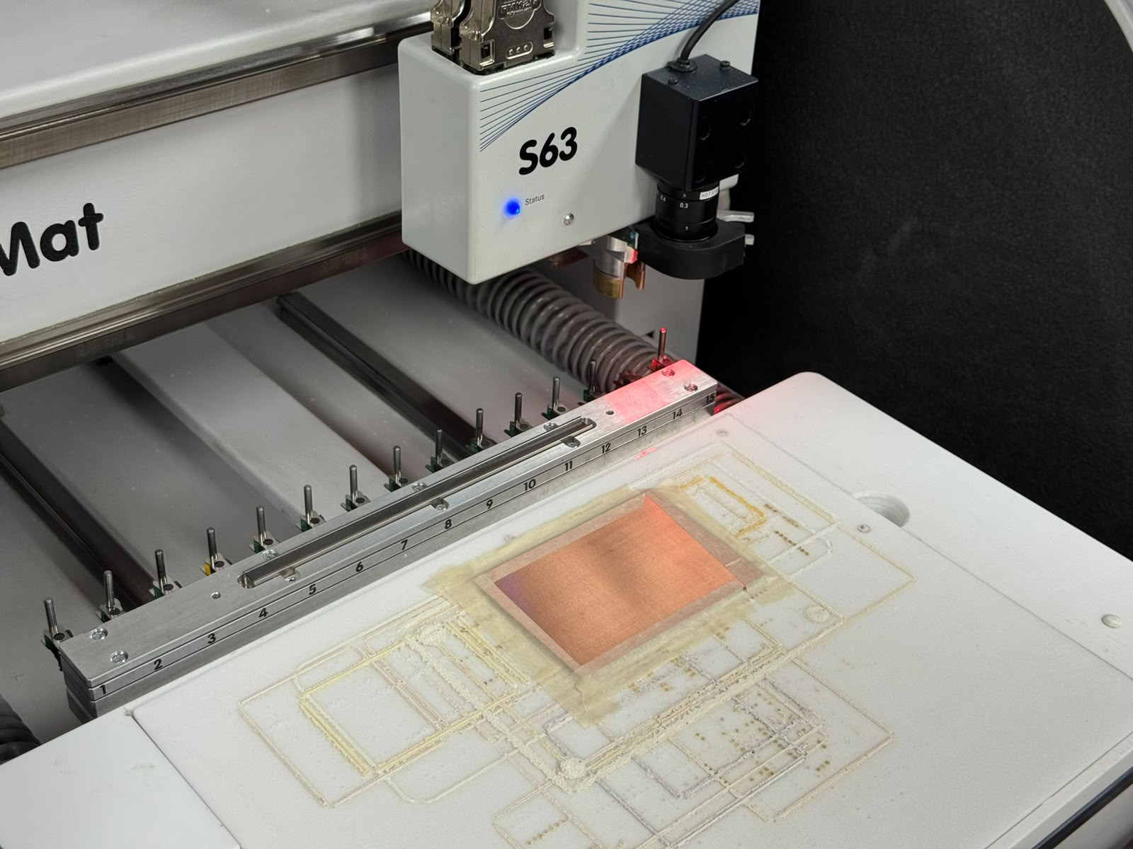
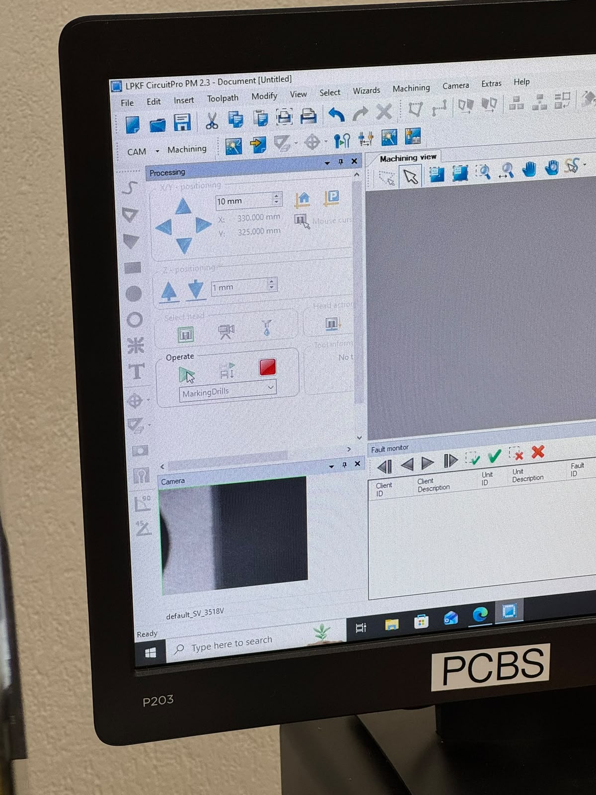
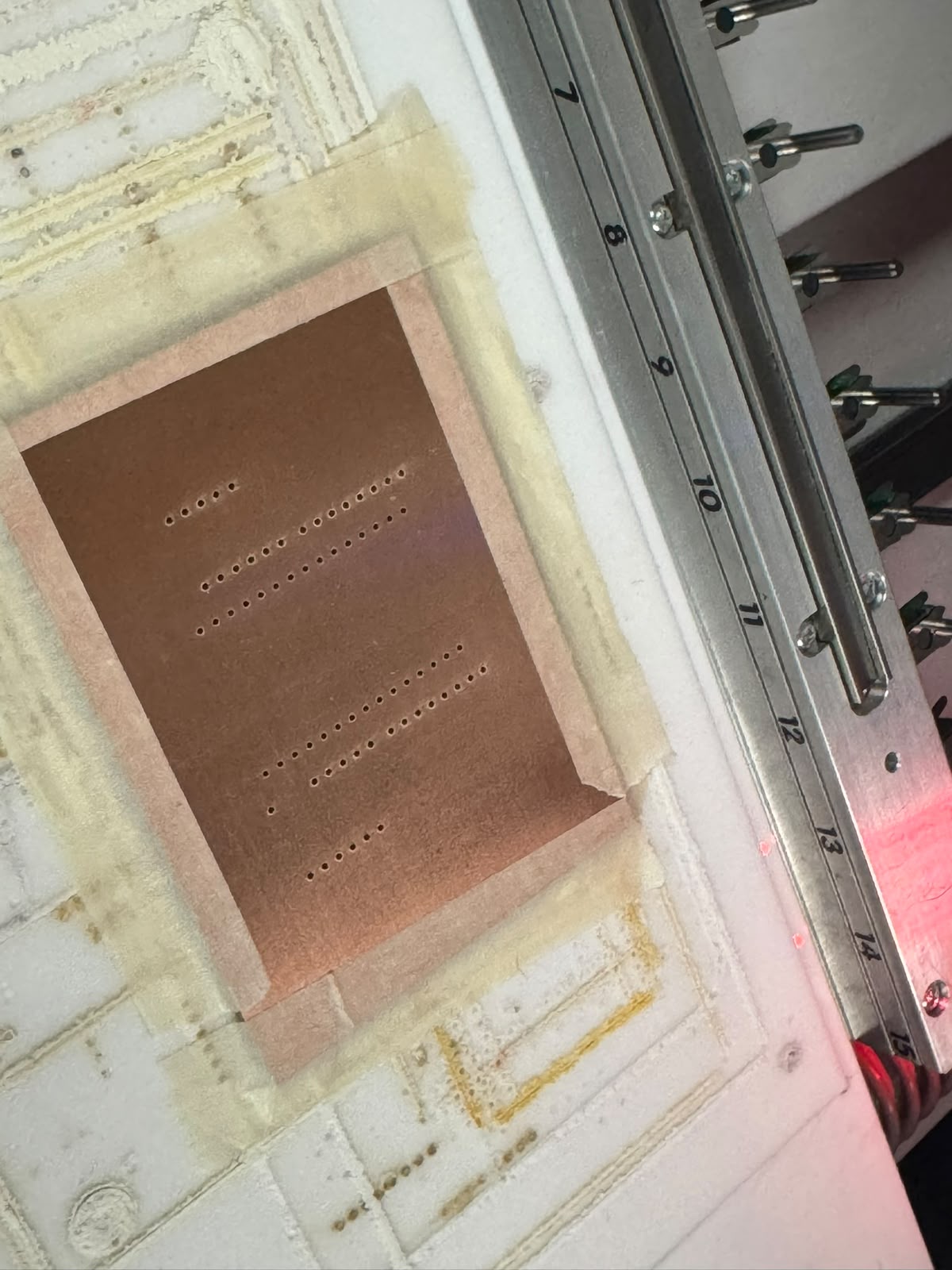
Then we selected the next process, and started the marking of the drills:
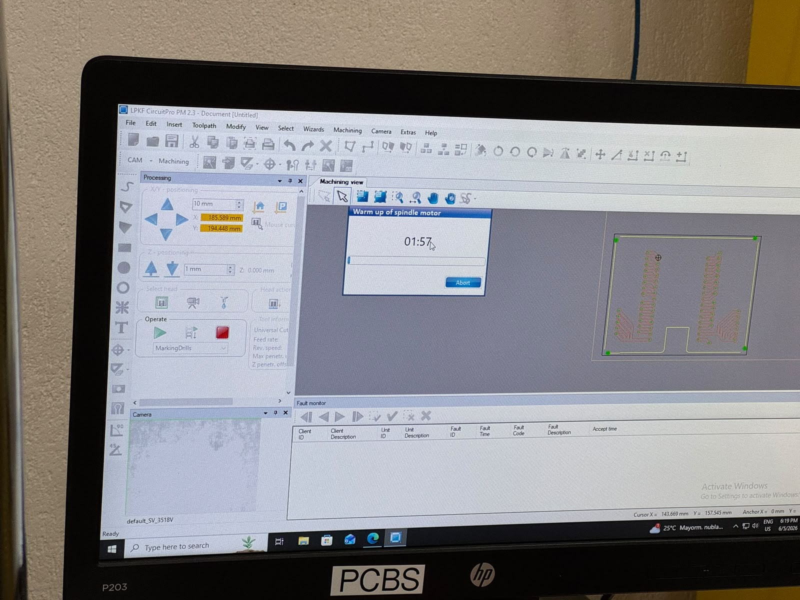
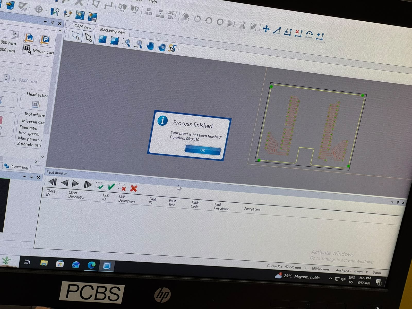
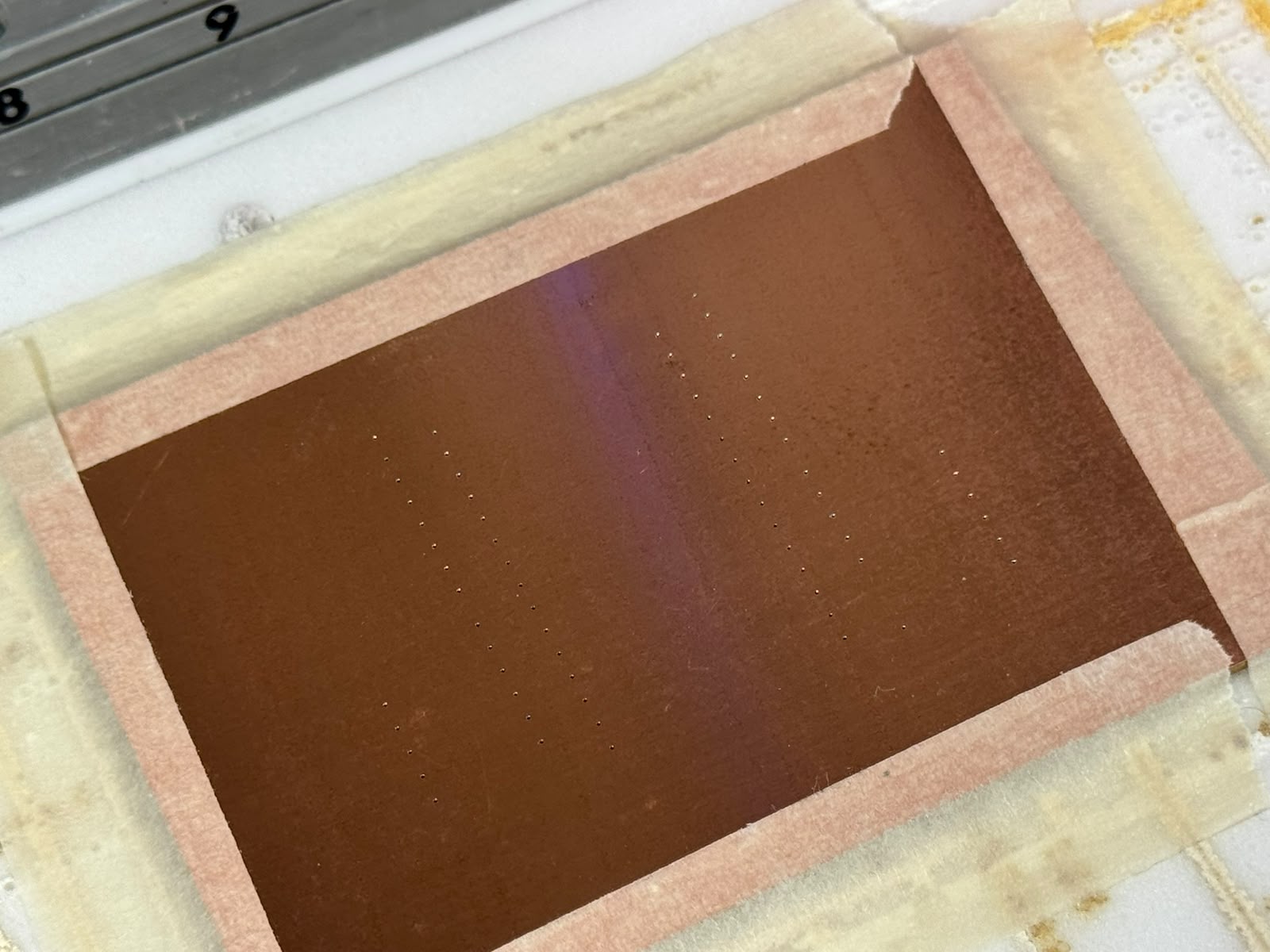
*Each time, the software notified when the process was done
After that, we selected the next process: drilling. For which the machine had to change tools:
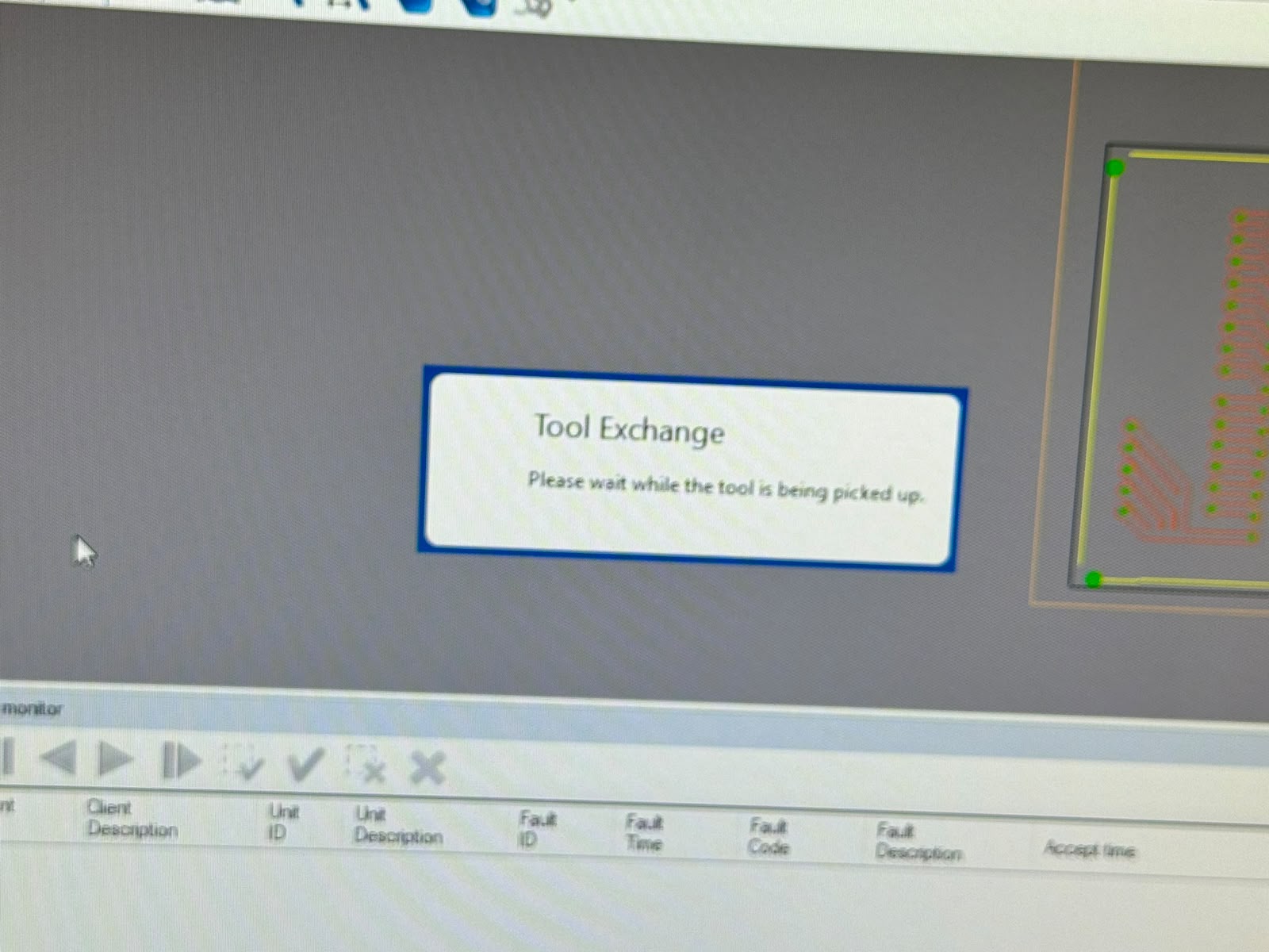
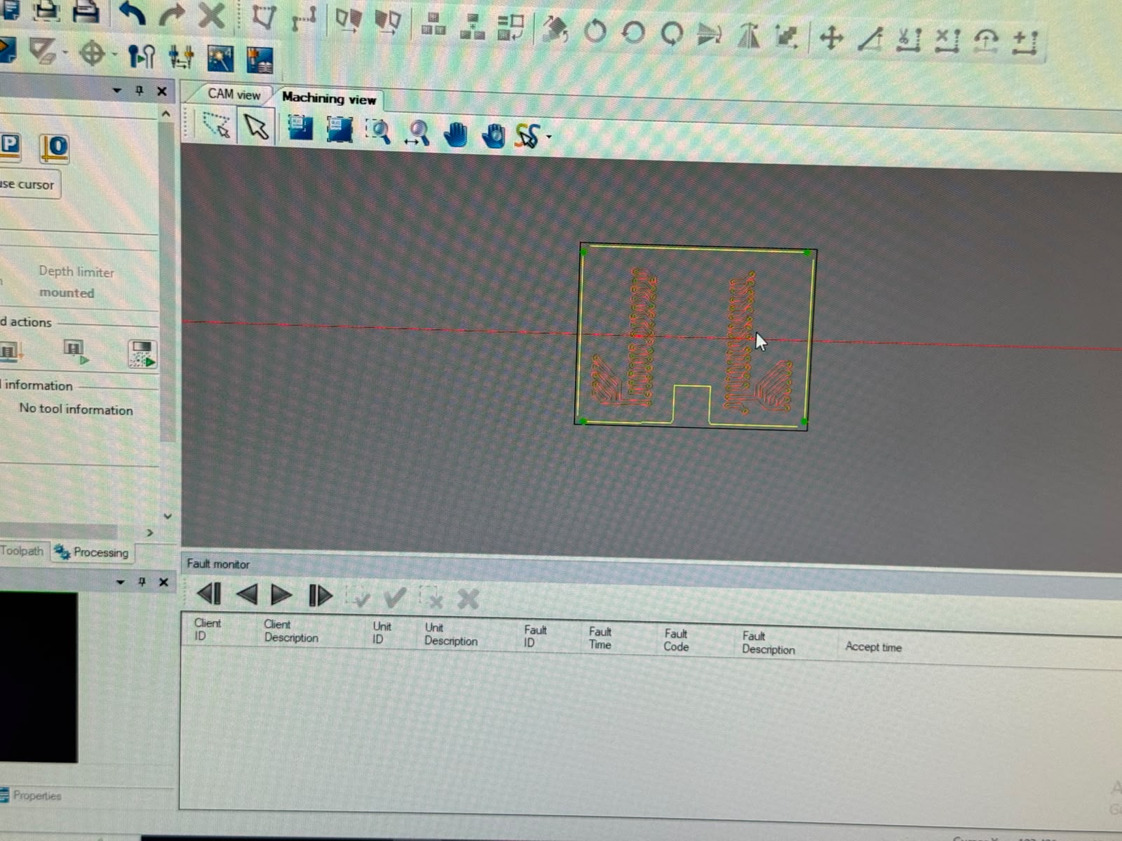
The next process was path routing. Again, the machine had to change tools and we could see the movements live on the software:
Finally, the last process was outline routing. A new tool was used and we were notified that the process was done.
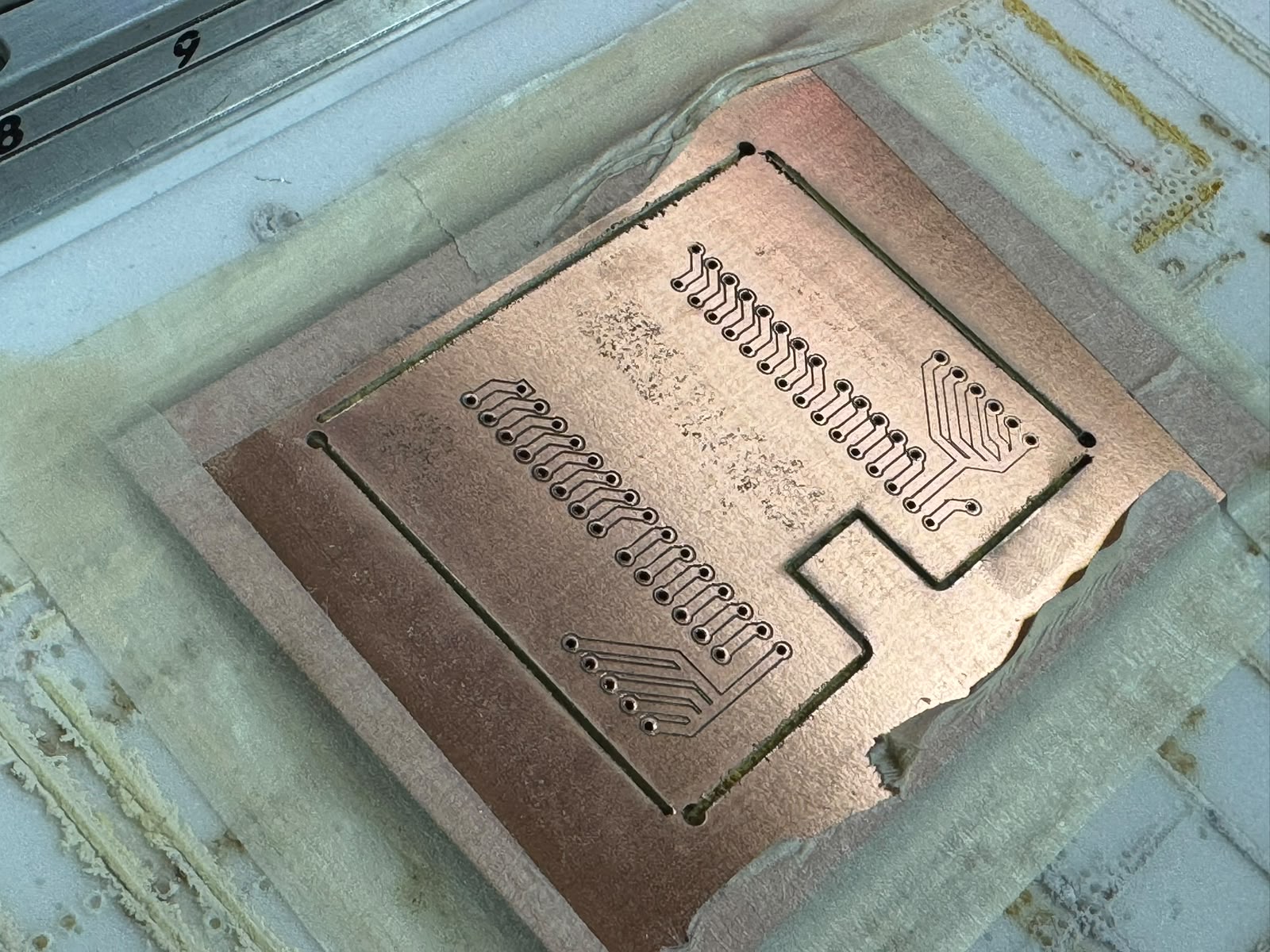
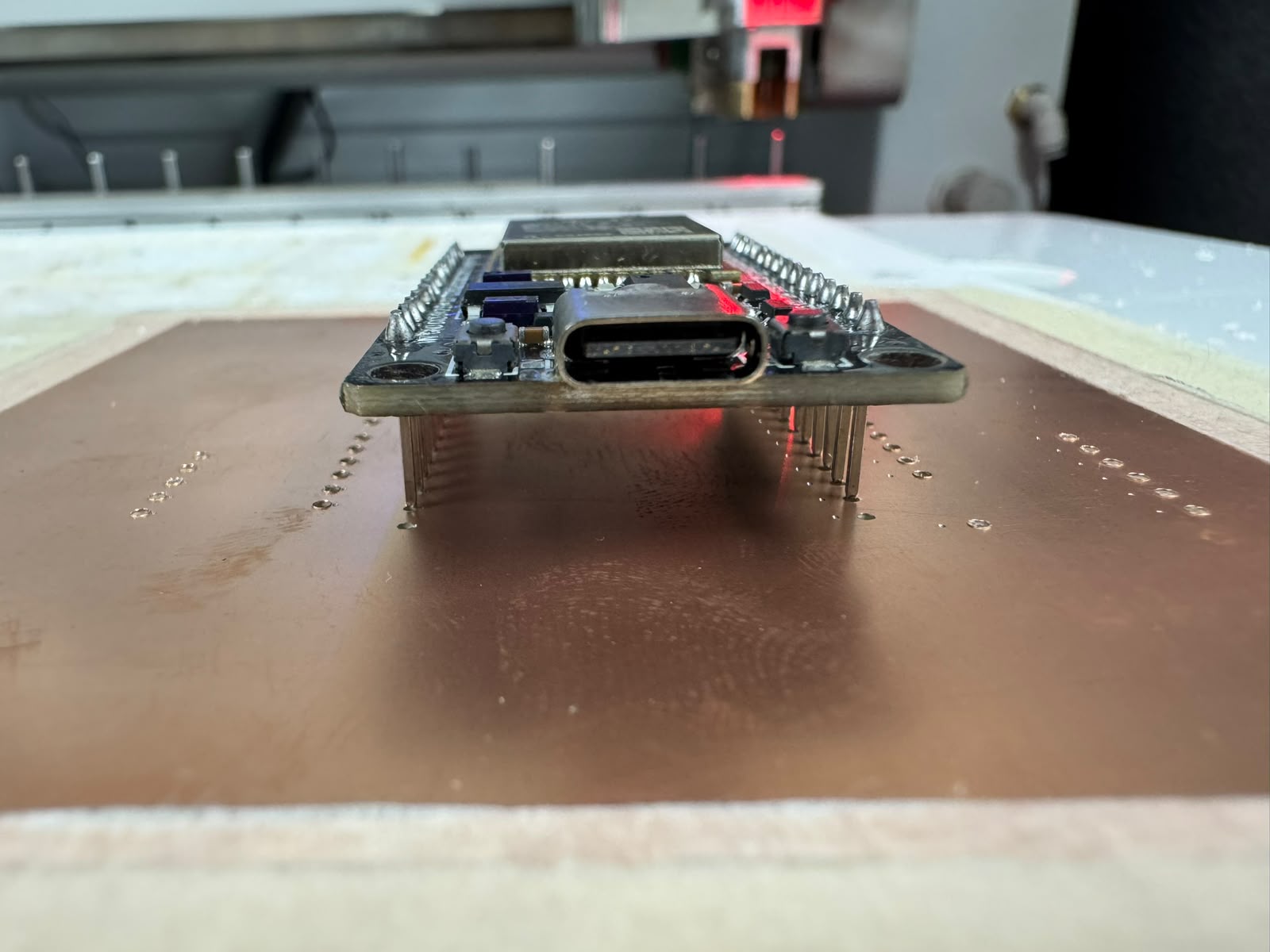
When the process finished, we cleaned the machine and tested the fit for the ESP32. IT DID NOT MATCH!!
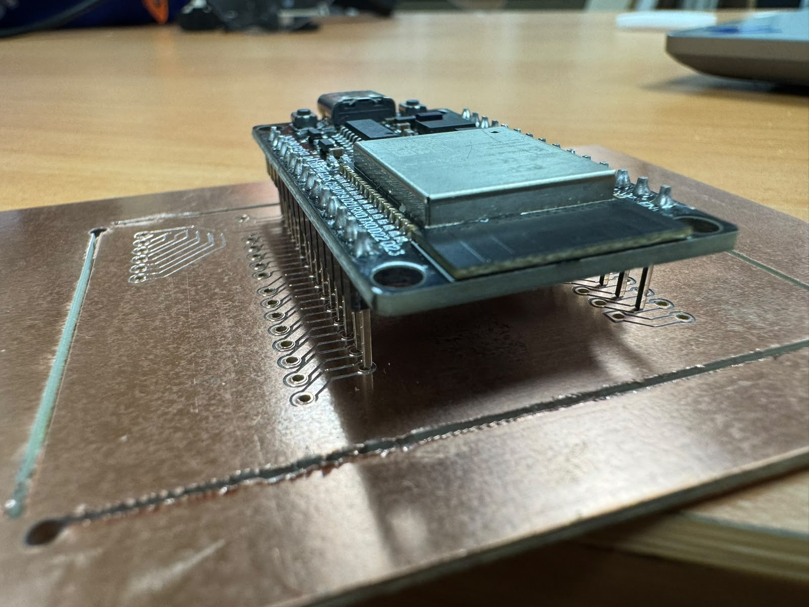
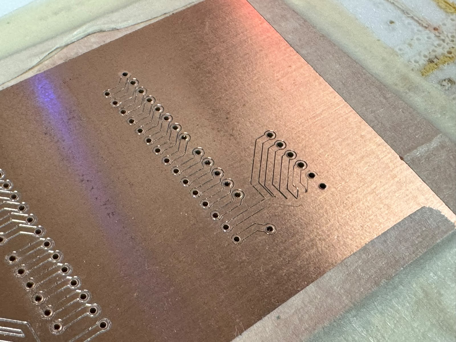
The drills on the left were too close to the ones on the right and some paths where not fully routed, so I had to go back, edit the desig and export all files again:
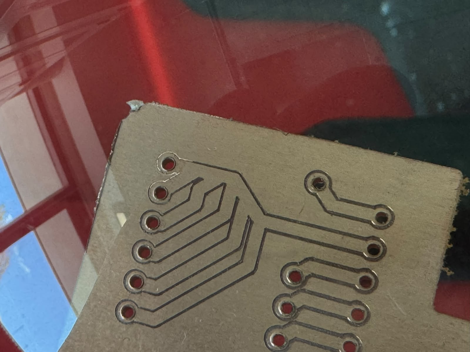
We ran all steps and processes again, checking along the way and resulting in a new functional board:
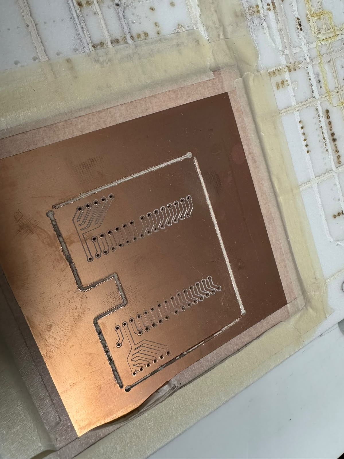
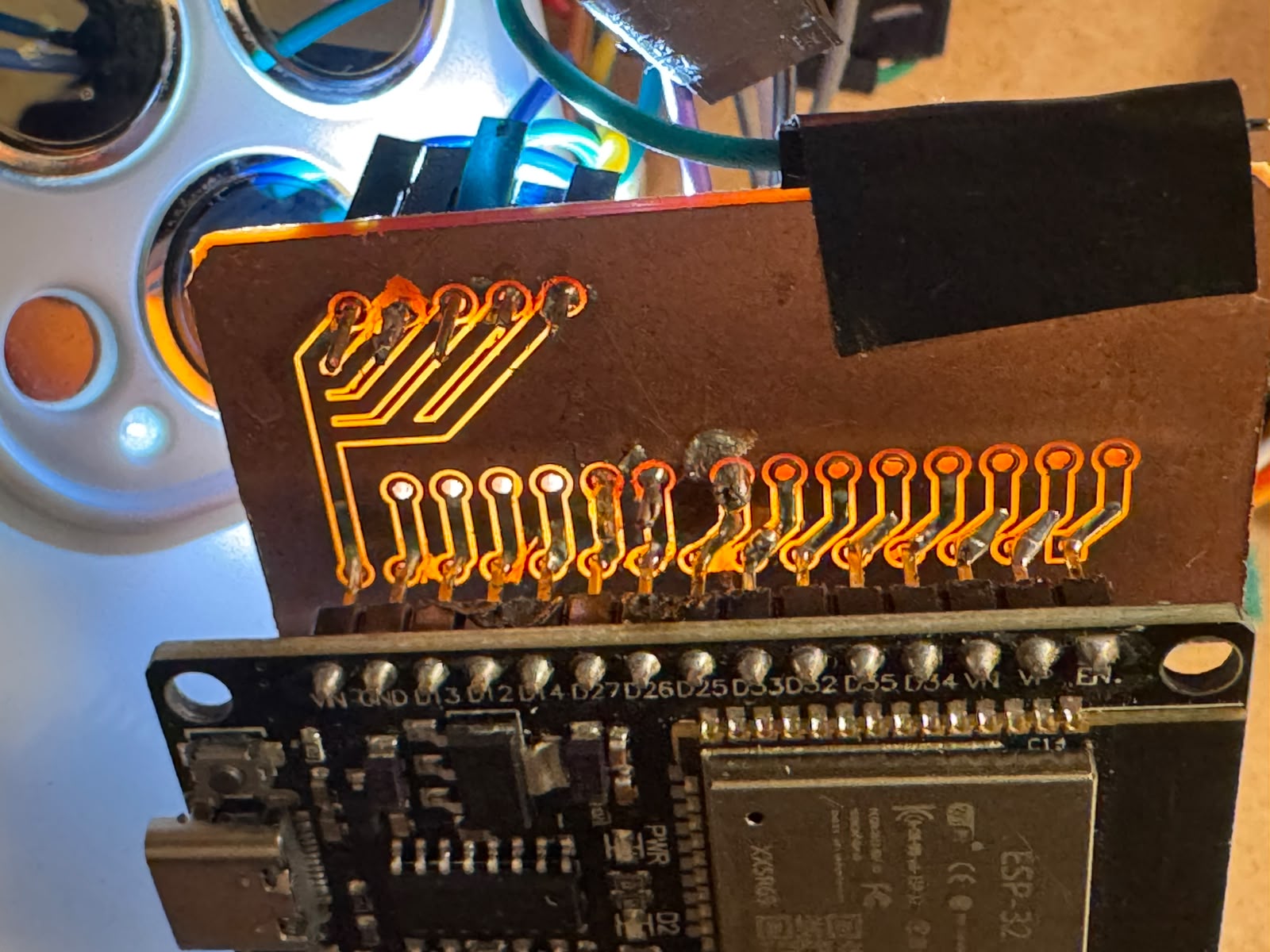
In the end, I manually corrected the spare PCB, used it to practice soldering and soldered all components:
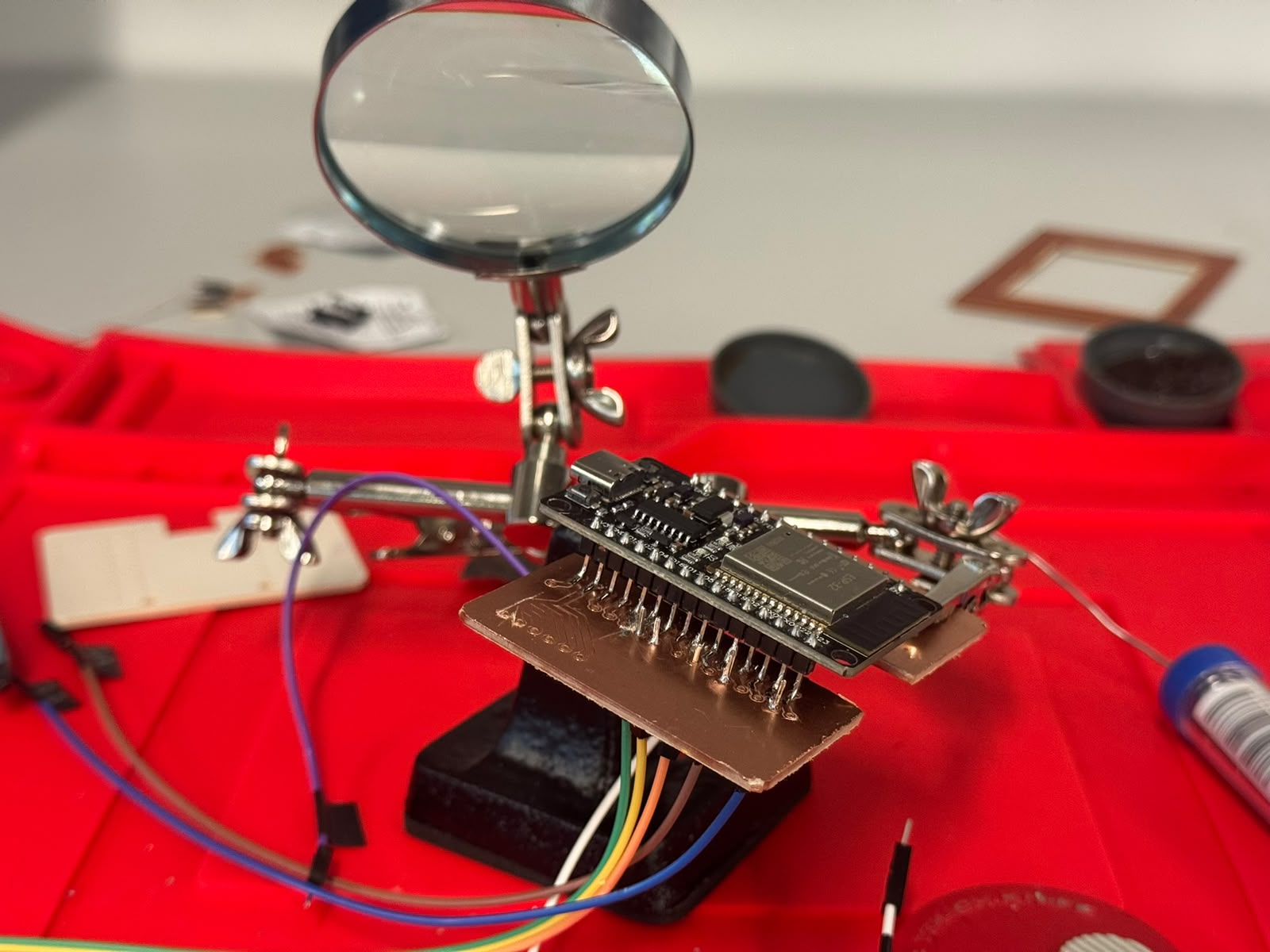
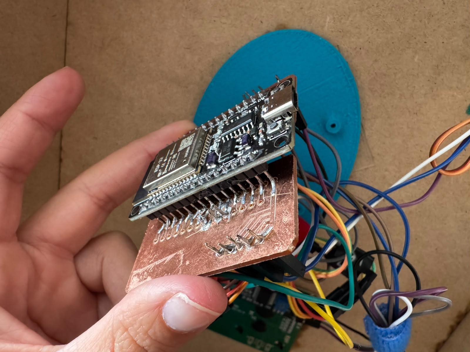
While soldering, I checked continuity in all pins in the ESP32, the PCB and each component. I had to clean and correct several times.
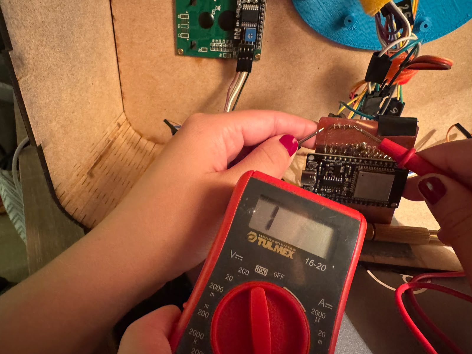
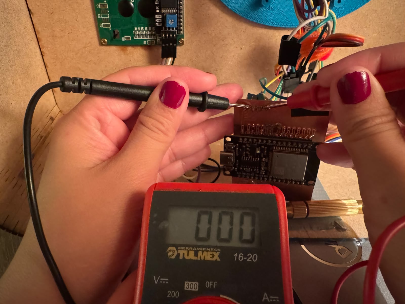
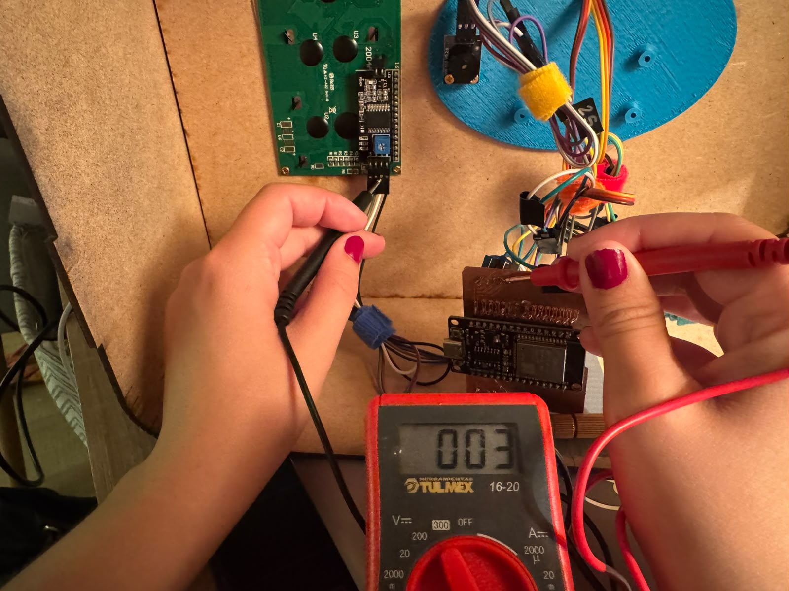
I also checked that all paths were clean with the help of light:
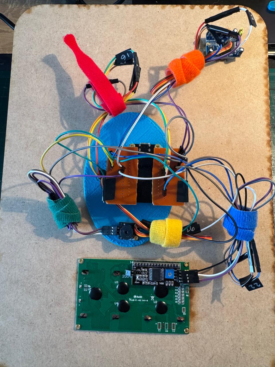
Finally I sorted all cables by component, marking with tape the pins that went to signal and left them a little long to be able to manipulate everything.
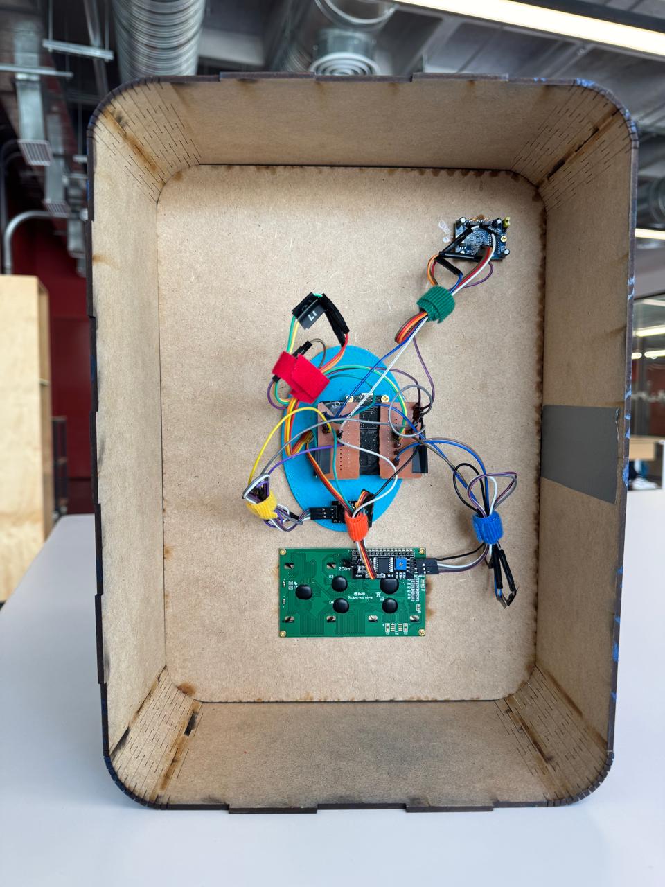
Go to the Final Project page to see the result of the PCB working.
Download all files