Week 6: Electronics Design
Electronic Design
Electronic design involves the development and integration of electronic components to achieve a desired functionality or performance within a product or system. This process includes research, schematic creation, printed circuit board (PCB) design, and prototype development to test and optimize the final solution.
Electronic design is a critical part of the product development lifecycle and requires a combination of technical knowledge, creativity, and strong problem-solving skills. It plays a vital role in industries such as consumer electronics, automotive systems, aerospace, telecommunications, and medical devices.
The discipline demands knowledge in circuit theory, electronic components, signal processing, and electromagnetic compatibility (EMC). Additionally, designers must consider factors such as power consumption, physical size, reliability, cost constraints, and regulatory compliance to ensure that the final product meets performance requirements and industry standards.
PCB
A Printed Circuit Board (PCB) is a board that mechanically supports and electrically connects electronic components using conductive copper traces embedded within insulating material layers.
PCBs are built by alternating layers of copper and non-conductive laminate. During manufacturing, unwanted copper is etched away to form the intended circuit traces. The layers are then laminated together to create the final board structure.
After fabrication, components are mounted on the outer layers. Surface-mount devices (SMD) are placed automatically, while through-hole components may be inserted manually or by machine. The board is then soldered using reflow or wave soldering. Finally, a solder mask and silkscreen are applied to protect the board and label component locations.
For more information i recomend to take a look at this webpage Good source.
Fabrication process of a PCB
| Step | Description |
|---|---|
| Step 1 | Place the conductive surface on the plotting machine (laser or CNC). |
| Step 2 | Transfer the design into the machine. |
| Step 3 | Placing the holes. |
| Step 4 | Multilayer lamination. Main drilling. |
| Step 5 | Track tracing. |
| Step 6 | Deburring and cleaning. |
| Step 7 | Solder components. |
Common PCB components
MicrocontrollersPower Sources.Resistors.Passive two-terminal electronic component that implements electrical resistance in a circuit.Diodes.Two-terminal electronic component that allows electric current to flow primarily in one direction. Transistors.Semiconductor that amplifies or change a signal.Analog.ALL.Basic Logic Components.NOTE: These components can be SMD (Surface Mounth Device) and Through-hole. Which means that some components are superficial and other need to be placed in a hole previously made in the board.FDM Materials
Kicad
KICAD
KiCad is a free, open-source Electronic Design Automation (EDA) software suite used to create professional schematic diagrams and printed circuit boards (PCBs). KiCad has a schematic editor, PCB Layout and a 3D viewer. It can be installed in the official website.

Adding a library
To add a library we must have already installed the program and open it.
Steps to add a library

1. In the initial menu, click on the section Plugin and Content Manager.
Steps
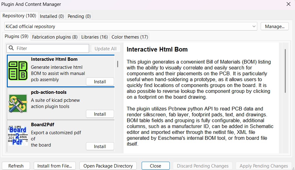
2.After clicking on the section, another menu will appear where we can see the Plugins and libraries supported by KiCad.
Steps
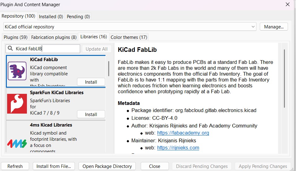
4. Finally, we must go to the Libraries section and write KiCad FabLib. The Fab Academy library will appear and we just have to click install.
Create a project
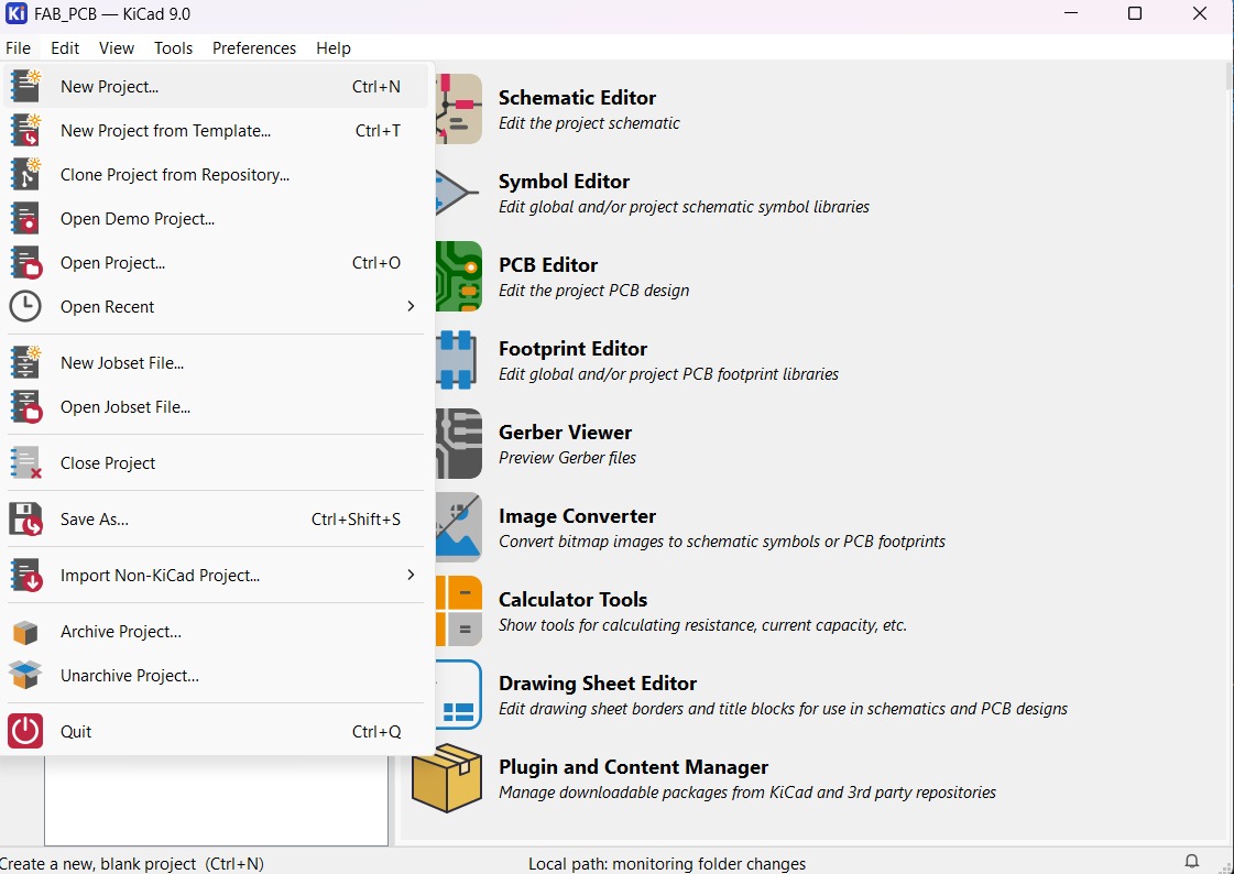
To create a new project we have to click on File placed in the top left corner and select New Project.
Steps to create a new project
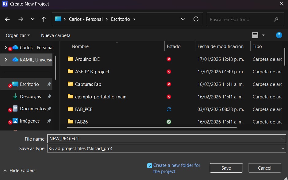
2.Subsequently, a Folder will be created. We will have to write the name of the new Folder and choose the place were it will be saved.
Steps to create a new project
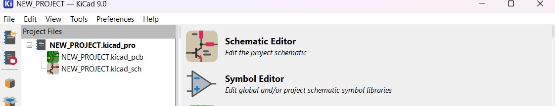
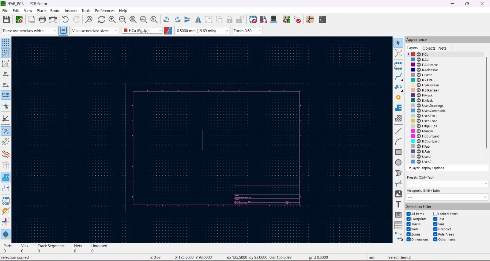
3.Finally, the new project folder will be added and the next step is design the Schematic.
Project Design
My projects name is FAB_PCB. To begin the desgin we have to select the Schematic Editor.
Schematic Design
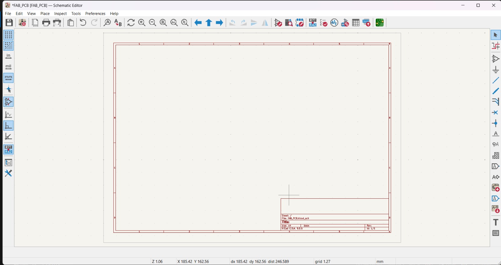
1. Once in Schematic Editor a board will appear.
Schematic Design
Top Tools

Top Tools
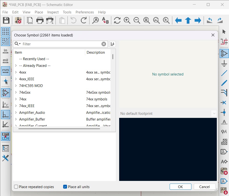
Save. Save changes.Schematic Setup. Edit the Schematic Setup.Page Settings. Edit the format of the page.Print.Print the page.Plot.Plot the page.Paste.Undo/Redo.Find/Find and Replace. Allows to find a component and replace it.Refresh.Zoom (5).Navigate (3).Rotate clockwise/counterclockwise.Mirror Vertically/Horizontally. Flip selected items.Symbol Editor. Create, Delete and Edit Schematic Symbols.Symbol Library Browser. Allows to watch the list of components included in the program and edit them.Footprint Editor. Create, Delete and Edit board Footprints.Symbol Editor. Create, Delete and Edit Schematic Symbols.Electrical Rulechecker. Runs a test(ERC) and looks for mistakes in the Schematic.Simulator.Shows the SPICE or IBIS simulation.
Schematic Design
Right Side Tools

Right tools are for the Schematic Editor section.
Right Tools
Select item. Allows to select items.Highlight Nets. Highlight wires and connections between items.Place Symbols. Place components.Place Power Symbols. Place Power and Ground Symbols.Draw Wires.Draw Buses.Place Wire to Bus Entries.Place No Connect Flags. To show the pins that don't have any use.Place Junctions. Place unions between wires and items.Place Net Labels.Assign Net tags to make connections.Place Directive Labels. Assign Directive tags to make connections.Place Global Labels. Assign Global tags to make connections.Place Hierarchical Labels. Assign Hierarchical tags to make connections.Draw Hierarchical Sheets. Draws a box of Hierarchical items.Place Sheet Pins.Sync Sheet Pins. Synchronize sheet pins and Hierarchical Sheets.Text.Add text.Draw Text Boxes. Draws a box with a label.Draw Tables.Schematic Design
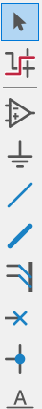
Left Side Tools

Left tools are for the PCB Layout section.
Left Tools
Show Grid. Display background grid in the edit window.Grid Overrides. Enables item-specific grids that overrides the current grid.Polar Coordinates. Switch between Polar and Cartesian Coordinates.Inches. Changes de board units to inches.Mils. Changes de board units to mils.Milimeters. Changes de board units to milimeters.Full-Windows Crosshairs. Switch display of full-window crosshairs.Constrain to H, V 45. Limits actions to horizontal, vertical or 45 degrees from the starting point.Show Ratsnet. Show lines or arcs that represent missing connections on the board.Curved Ratsnet Lines. Show ratsnet with curved lines.Inactive Layer View Mode. Toggle inactive layers between normal and dimmed.Draw Zone Fills. Show filled areas on board.Draw Zone Outlines. Show only zones boundaries.Sketch Pads. Show pads in outline mode.Sketch Vias. Show vias in outline mode.Sketch Tracks. Show tracks in outline mode.Appearance. Show/Hide the appearance manager.Schematic Design Steps
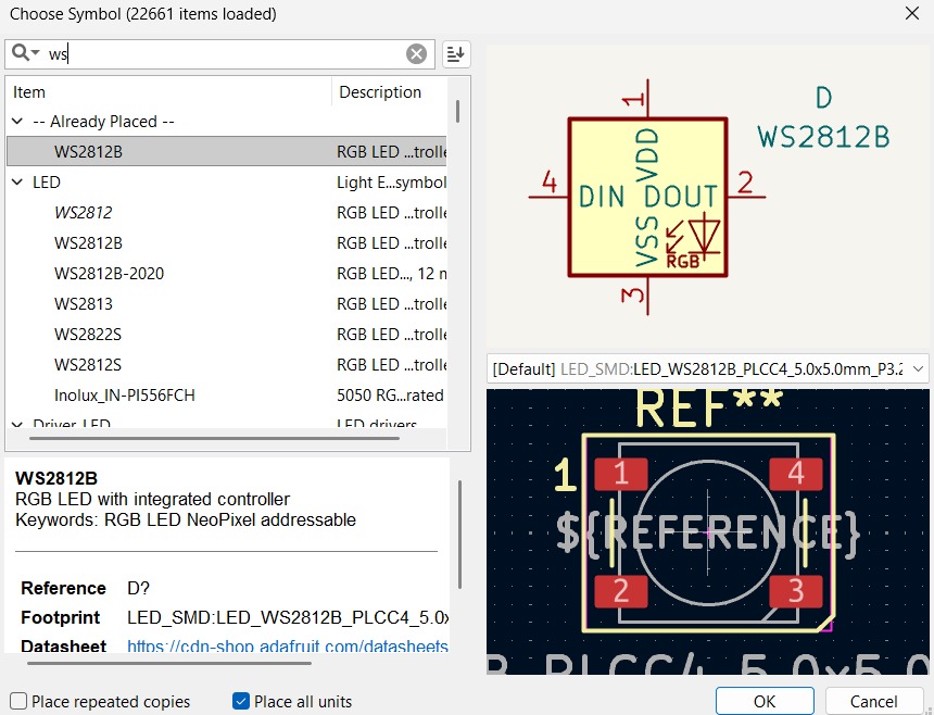
1. First, we have to add the components we intend to use with the Place Symbol tool.
Choose Symbol.A menu will appear, with a search engine and a list of components on the left-hand side. On the right-hand side, you can see the symbol and footprint of the components you select. It is preferable to select those that have a symbol and footprint.
Schematic Design Steps
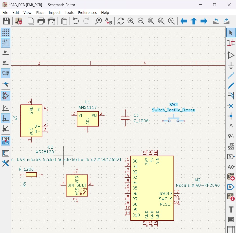
2. Then place the components on the board. I used only components that are in the Fab library.
My components
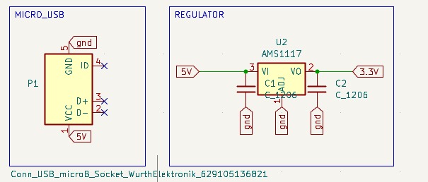
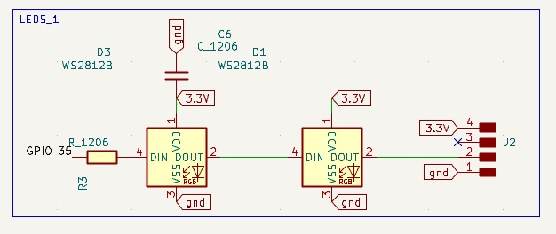
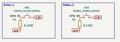
Micro USB. It will act as my power source.AMS1117. It is a power regulator that recives a 0 - 12V input and gives an output of 3.3V that I used to power my circuit. AMS1117 Datasheet.WS2812B. It is a intelligent control LED light source that the control circuit and RGB chip are integrated in a package of 5050 components. It internal include intelligent digital port data latch and signal reshaping ampli fication drive circuit. WS2812B Datasheet.4 pins button. It is a button with four pins, 2 connected linealy between each other.XIAO RP2040. It is a small microcontroller that carries the powerful Dual-core RP2040 processor that can flexible clock running up to 133 MHz which is a low-power microcontrollers. On the Seeed Studio XIAO RP2040 there is also 264KB of SRAM, and 2MB of on-board Flash memory which can provide more program to save and run. On the other hand, this little board has good performance in processing but needs less power.XIAO RP2040 features.1206 Ceramic Capacitor. It is a passive, two-terminal electronic component that stores electrical energy temporarily. 1206 SMD components typically meassure 3.2mm X 1.6mm (0.126 X 0.063 inches).1206 Resistor. It is a passive, two-terminal electrical component that implements electrical resistance to limit or regulate the flow of electric current in a circuit.
Schematic Design Steps
3. Then I added the corresponding connections according to my purpose.
Power and regulation.To power my circuit, I placed the micro USB port and connected it using two global ground and 5V labels, which is the initial voltage I intend to supply to my circuit. I left the other pins, which are for data transfer, with a No connection flag, indicating that they will not be used.
To regulate and reduce the initial voltage I used the AMS1117. It requieres two capacitors for device stabilty, one in the input an one in the output. Both of them of 10µF.
LED arrangment. for the LED arrangement, I selected WS2812Bs because they are RGB and can change color through programming. I connected them to a pin on my Xiao using a resistor and a label, then connected the LEDs in series and the first power pin to a capacitor of 100 nFfor component safety. Finally, I left some holes so that more LEDs could be added if desired.
Schematic Design Steps
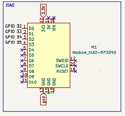
XIAO RP2040. I connected the XIAO to the output voltage given by the AMS1117 and to the global ground. I also connected the LEDs to one pin of my XIAO and my buttons to its respective pin.
Buttons. The arrange of the buttons is pull-down, in order to read 0 while not clicking on it and read active while clicking it. The buttons are connected to one 10k Ohms each.
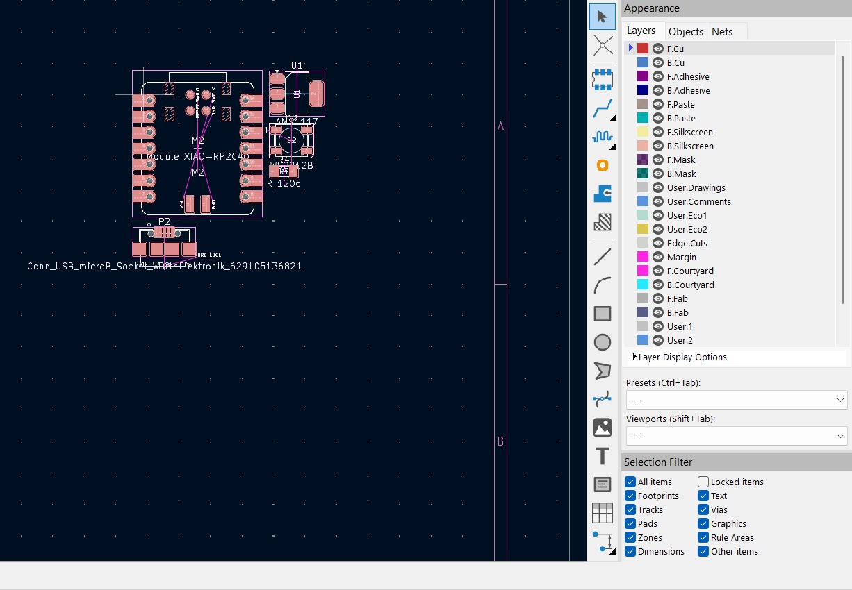
PCB Design
1. In the top menu of the Schematic Editor on the far right is a green symbol that opens the PCB Editor.
Most important tools for PCB edition
Top tools
Footprint Editor. Create, delete and edit a footprint.Footprint Library browser. Display the full list of components footprints.3D Viewer. Show 3D viewer window.Update PCB from Schematic. Update PCB with changes from Schematic.Design Rule Checker. Opens the rule checker window.Switch to Schematic Editor. Return to the Schematic section.Scripting Console. Show the Python scripting console.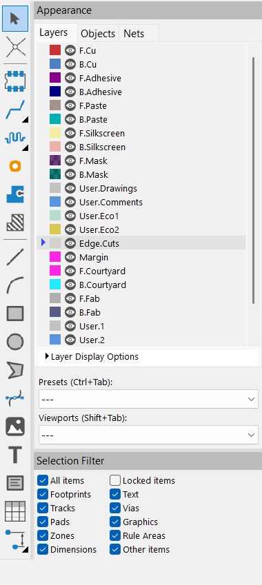
Right tools
Select Item.Local Ratsnet. Display the full list of components footprints.Place Footprint. Toggle Ratsnet display of selected components.Route single track. Wires the components.Tune lenght of a single track.Place Vias.Draw Filled Zones.Draw Rule Areas.Draw Polygons.Draw Bezier Curves.Place Reference Images.Add bitmap images.Draw Text.Draw Text Boxes.Draw Tables.Draw Orthogonal Dimensions.Layers.Determine the layer where the path will be.Objects.Sets the opacity and which elements of the PCB can be seen.Nets.Establishes the networks of the components and their visualization.PCB Design
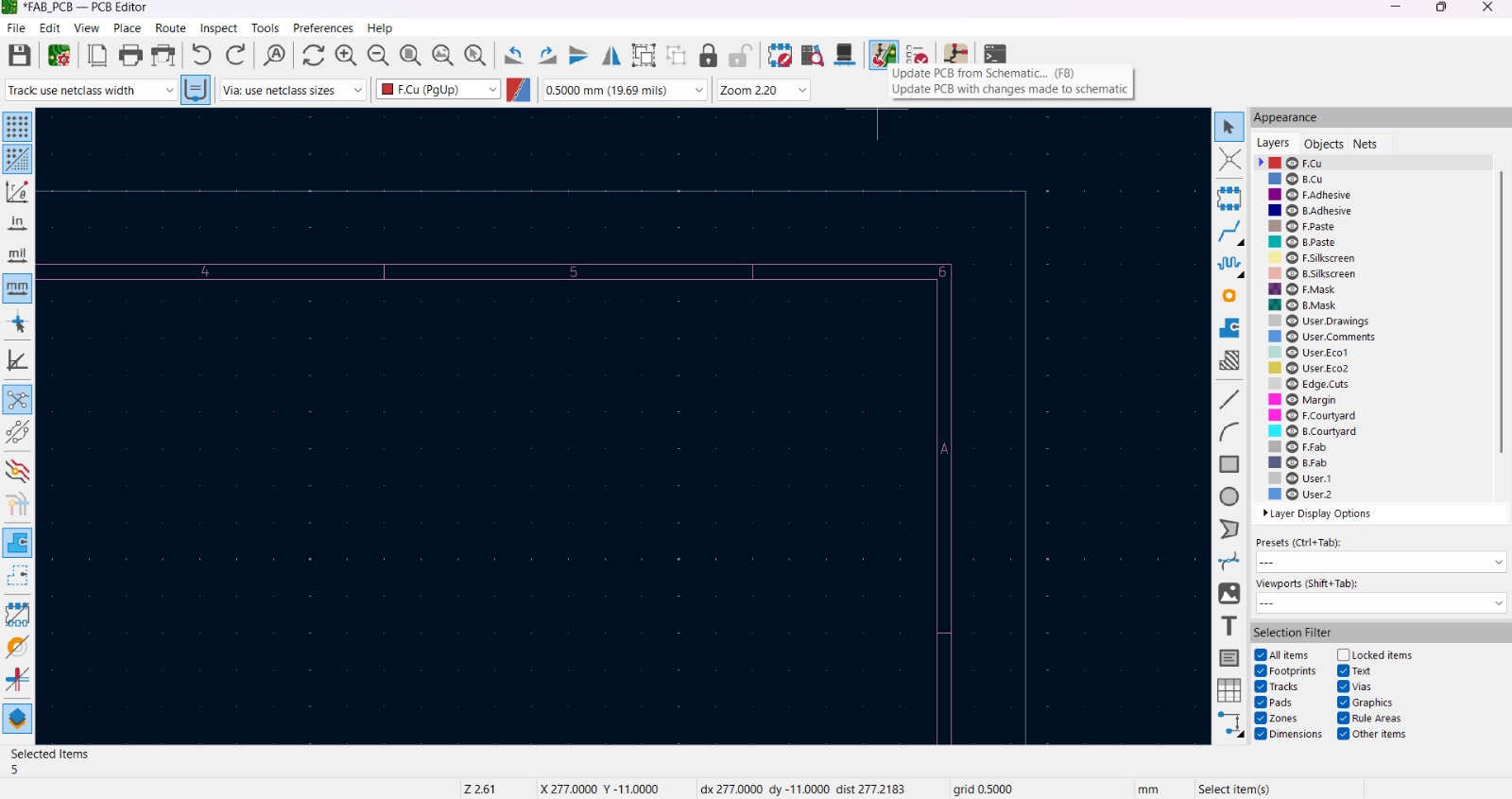
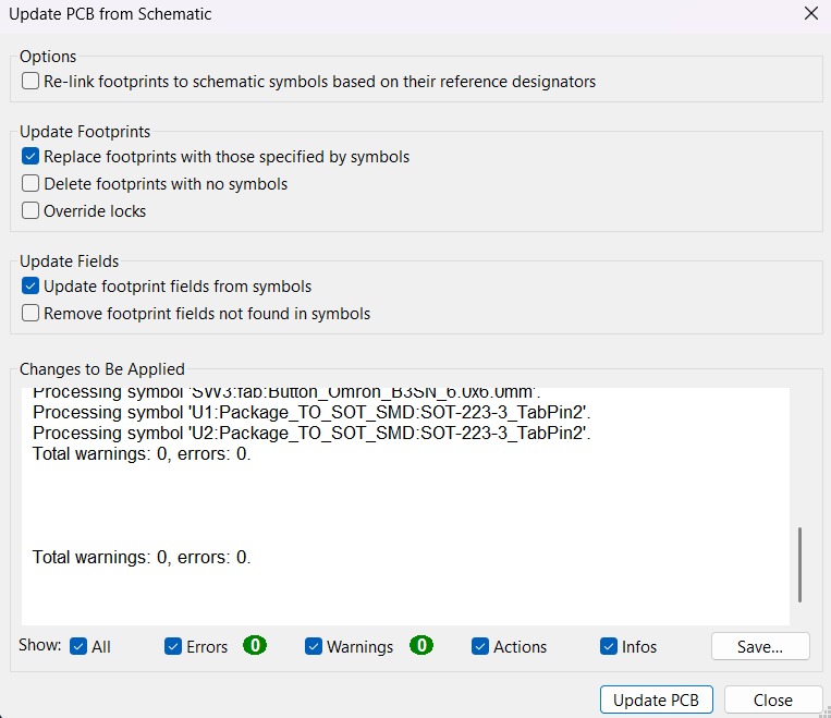
2. In the PCB Editor, using the Update PCB from Schematic tool the components can be added or updated.
PCB Design
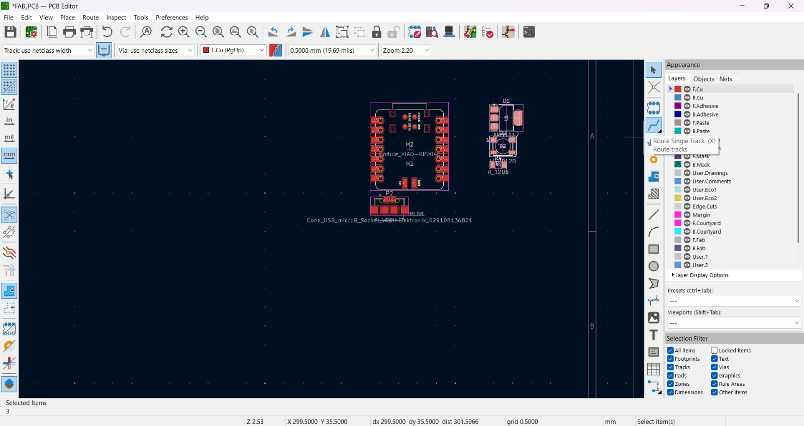
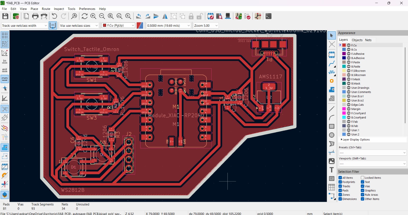
3. Then, using the Route single track tool, we can route the electronic connections between components.
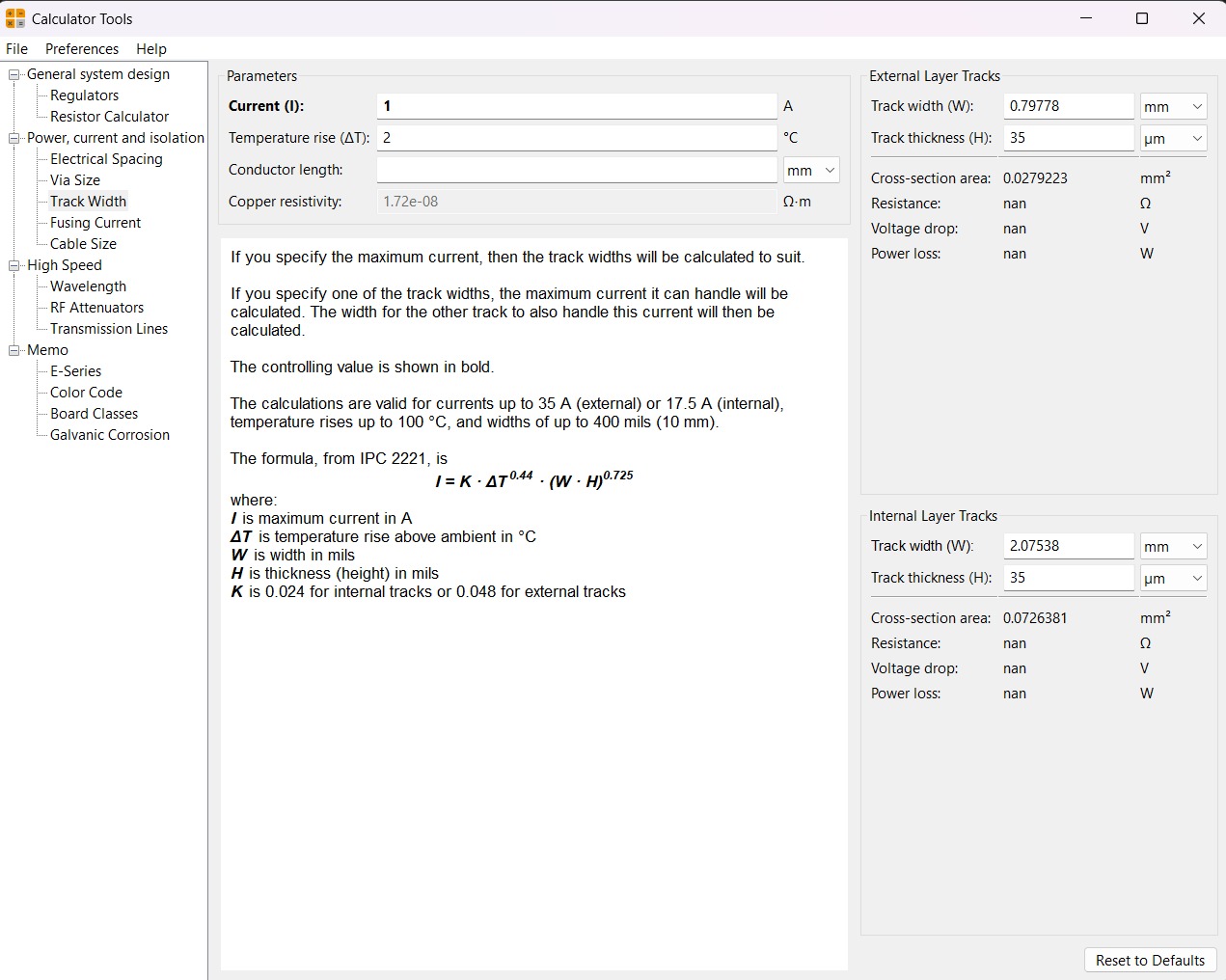
Calculator tool. Before defining the size, it is important to calculate it using the calculator tool given by KiCad. To do that we first have to go to the start menu and open the Calculator tool.Then add the Current (I) and the Temperature rise we are expecting our PCB to have and look fo the result the calculator will give back to us in the right top side. The calculator works by using a formula explained at the bottom.
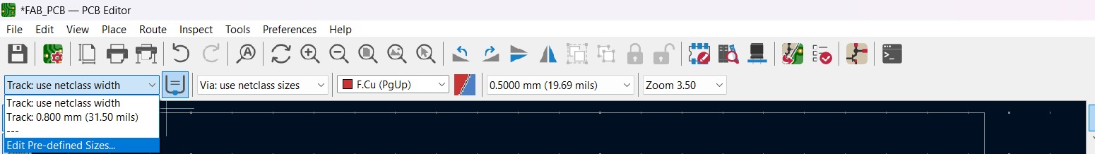
Track thickness. To change the track thickness we must go to the top tool section and click on Track use netclass width. Subsequently, select Edit Pre-defined Sizes.
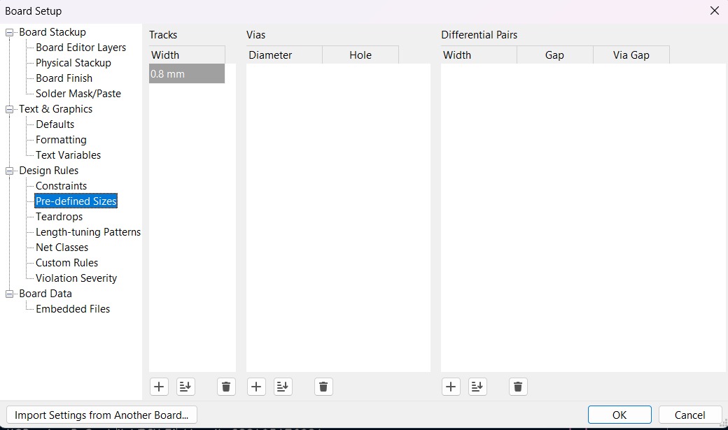
Track thickness. Inside that section we can add tracks sizes by clicking the + symbol located at the bottom of the window, and in the width section we can change the width of the new track we added. Then we'll just have to click Ok.
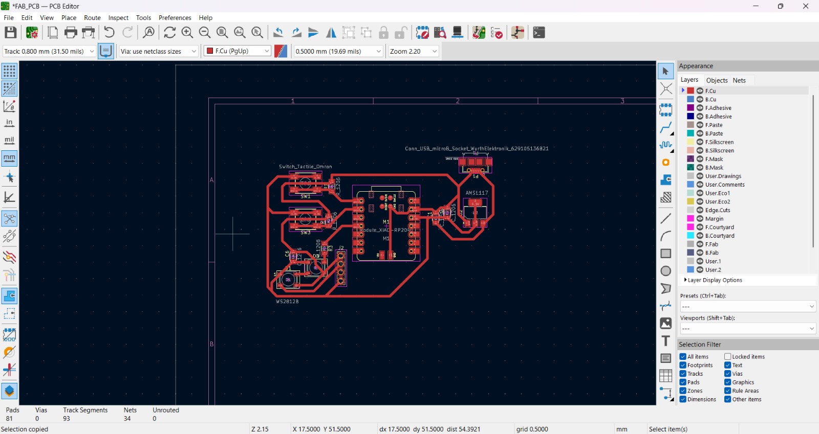
PCB Design

4. Then we have to choose the thickness we have already created and start connecting the components. KiCad will show us where we should connect our items, so it is very intuitive. For default the net where the tracks are is F.CU, we must left it there because that is what the program interprets as the tracks.
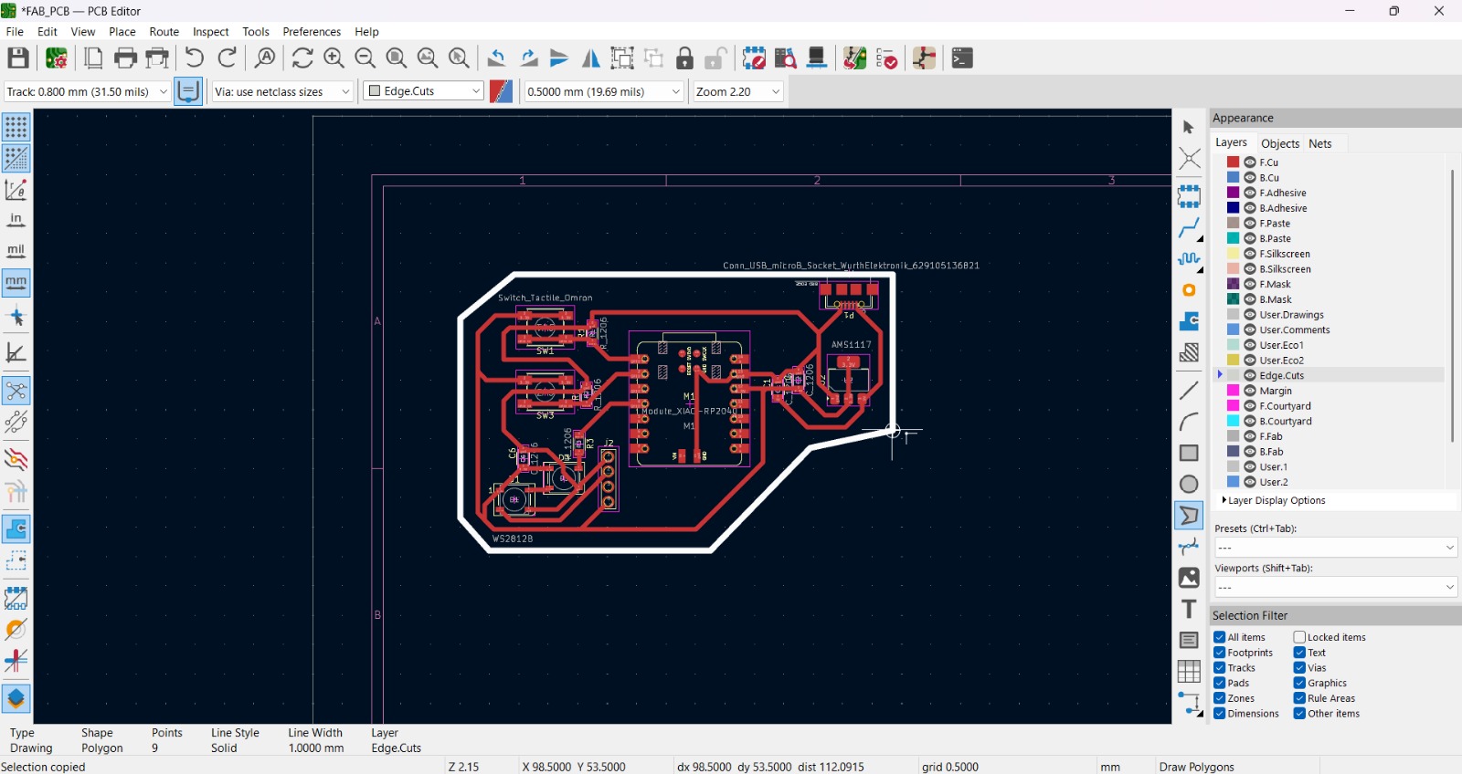
5. After tracing the tracks between our items, we have to draw the border of the PCB. For that we have to use the Draw Polygons tool and surround our items. We must change the net to Edge.Cuts.
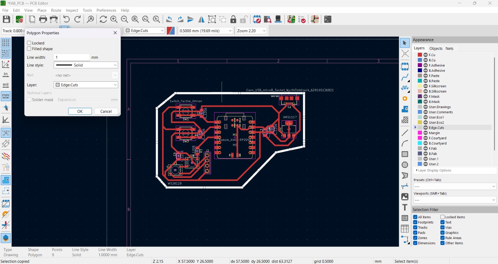
6. Then we have to change the width of the polygon by right-clicking the shape and selecting properties. I use a width of 1 mm.
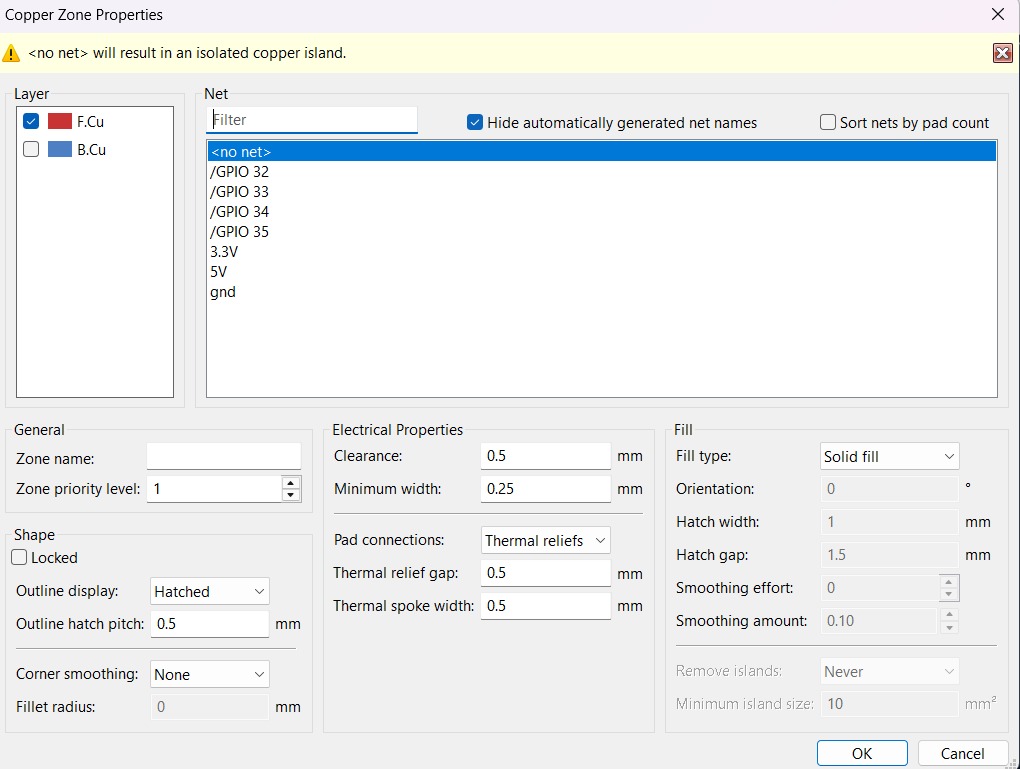
7. Finally we have to add a filled zone. to do that we have to use the tool with that name and draw it inside the PCB, then a window will appear and we'll have to leave it without any net.
PCB Design

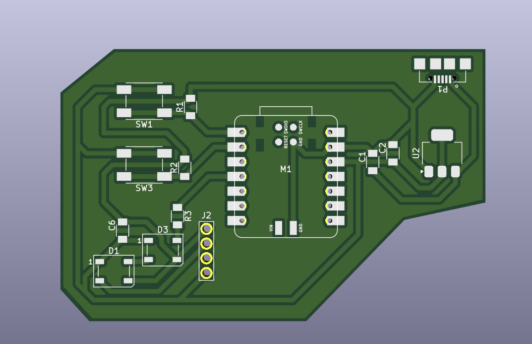
8. see how the PCB will look, we have to use the 3D Viewer.
NI Multisim
NI Multisim
NI Multisim is a powerful industry-standard SPICE simulation and circuit design software developed by National Instruments.

Schematic
1. We have to open NI Multisim and a board will open.
Schematic

2. Above is a bar with components to simulate. We have to click on the symbols to choose thwe type of component we want to use.
Component bar
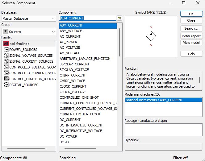
Source. The source components are the ones that power the system. In the left side list we can choose a specific type of component, in the center top we can search for a specific component of the family and in the right side we can see the symbol and place the component in the board. This repeats in each section.
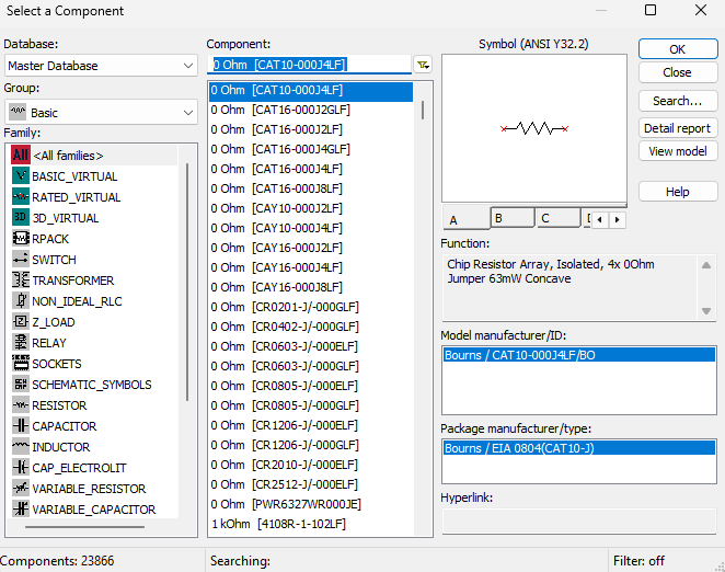
Basic. These are the basic components such as resistors, buttons, capacitors, etc. We can select the specific family in the left list.
Component bar
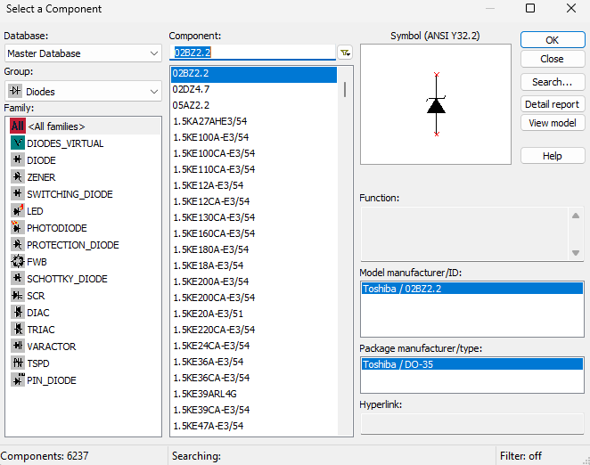
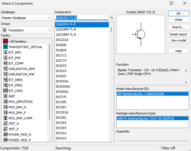
Diodes. A diode is an electronic component that allows current to flow in only one direction, making it essential for various applications in electronics. We can select LEDs, SCRs, FWBs.
Transistors. These are the basic components such as resistors, buttons, capacitors, etc. We can select the specific family in the left list.
Component bar
Diodes. The source components are the ones that power the system. In the left side list we can choose a specific type of component, in the center top we can search for a specific component of the family and in the right side we can see the symbol and place the component in the board. This repeats in each section.
Transistors. A transistor is a semiconductor that amplifies or switches electronic signals. Transistors serve as the basic building blocks of modern electronics.
Component bar
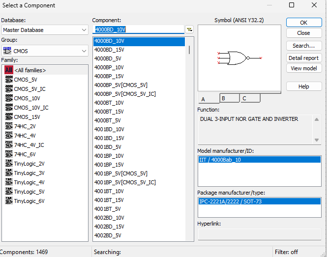
CMOS. Stands for Complementary Metal-Oxide-Semiconductor, a technology used to build low-power, high-efficiency integrated circuits and microchips.
Schematic
3. After understanding where the components can be selected and placed, we must begin with the schematic.
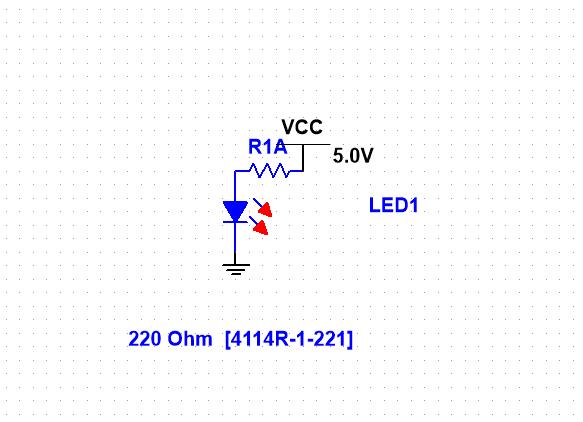
Components for this example:Red LED
220 Ohm resistor
220 Ohm resistor
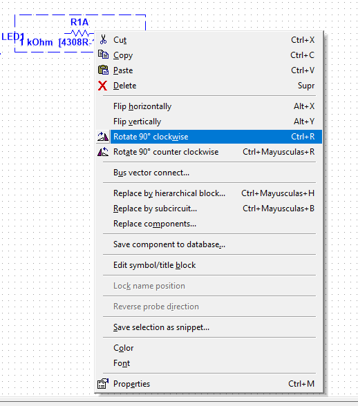
First we have to select the components, then place them in the board and if we want to rotate them we have to click the component and press CTRL + R.
Schematic
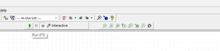
4. Finally we have to press the green triangle to simulate the circuit.
Simulation
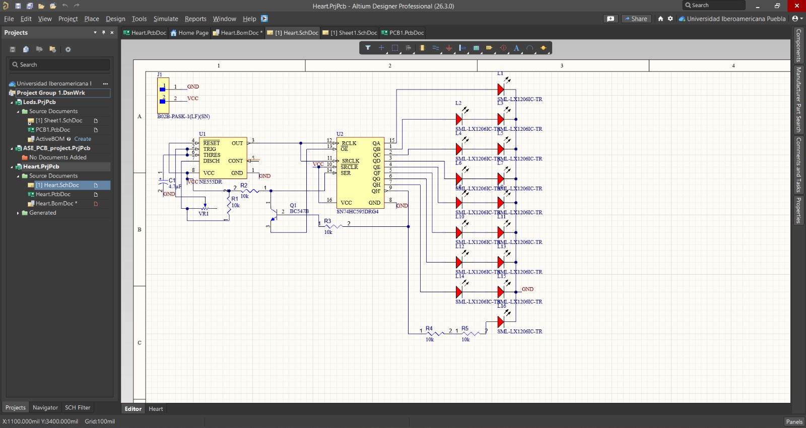
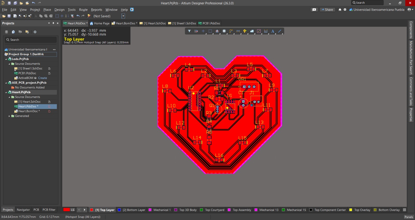
1. To simulate I'll use an ALTIUM Design I made a time ago.
ALTIUM is a comprehensive PCB and electronic design automation software package that allows engineers to design and customize their own circuit boards. It is similar to KiCad, but it isn't free and you can do a lot more things like simulate from there. But this time I'll use NI Multisim.
Learning outcomes
This week I learned a lot about PCB design. I had made printed circuit boards before, but I had never used components like the WS2812B, the microUSB port, or the AMS1117 voltage regulator. I came to understand the importance of capacitors in protecting components and preventing voltage spikes, and above all, the importance of properly arranging components on a board to make it truly efficient.