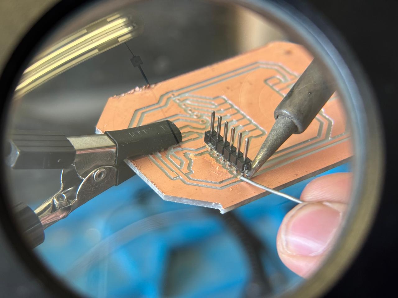
For component soldering,
there is no specific technique that must be followed. However, I recommend soldering from the smallest components to the largest, to avoid collisions or limitations in the working area.
During this week, the design of a PCB board was carried out, it was manufactured and tested to verify the correct procedure involved in PCB creation. Without a doubt, it is important to remember that circuit design was learned for the creation of this board, so this week it is extremely necessary to include this knowledge and apply it in a functional prototype.
During this week, the following phases can be observed:
First, to create the PCB board it is necessary to think about what you want to do and what the purpose of the PCB is. Based on this, I decided that my design should include LEDs, since I consider them to be some of the most basic components that can exist, but that can be used creatively (such as for indicating things). Likewise, my board needed to have pins to connect external elements if needed. Finally, I added a button and the corresponding resistors.
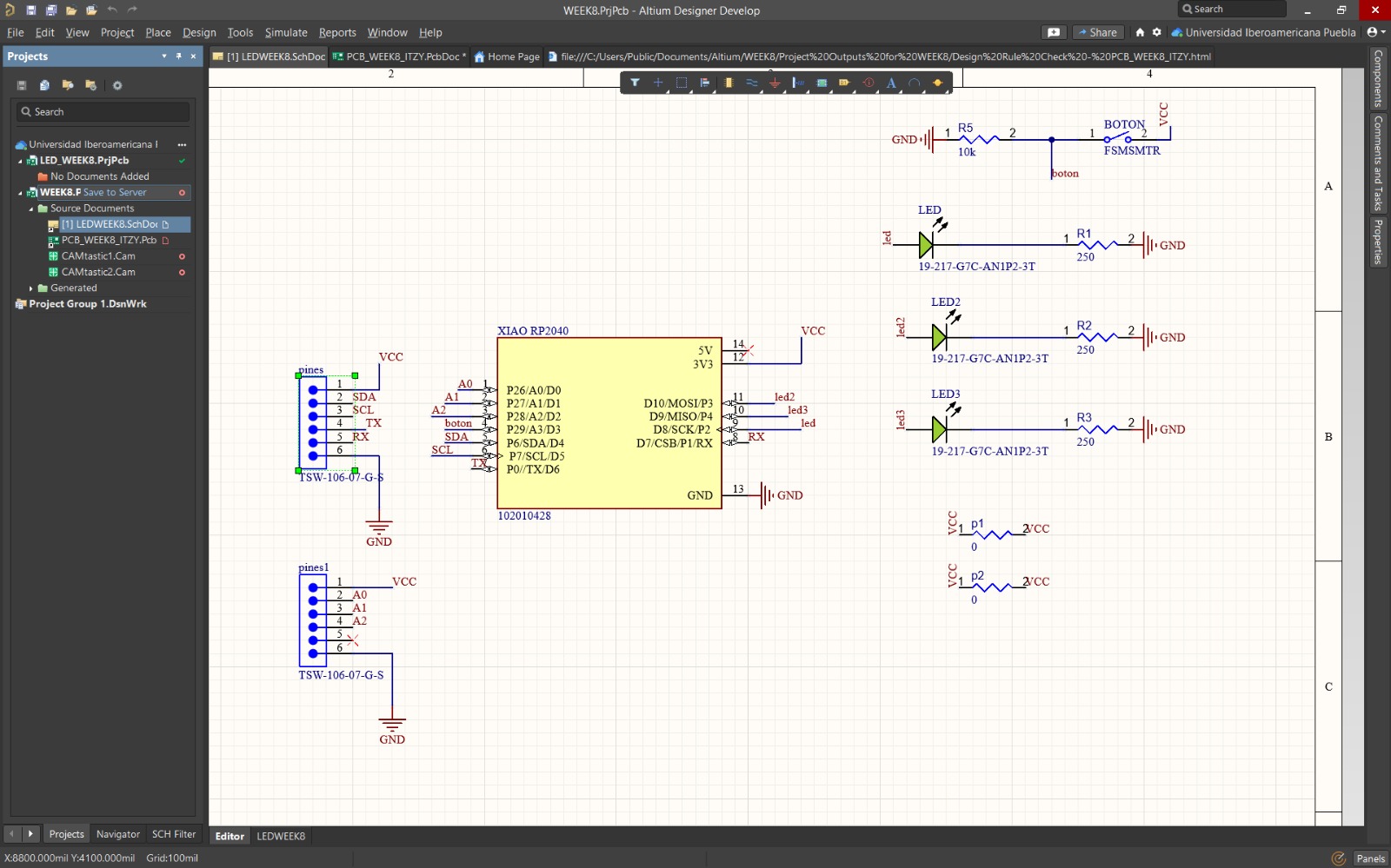
The microcontroller I would use was a XIAO RP2350. From this, considering the pinouts of this microcontroller, I placed them according to what I might need. For this, I considered digital and analog pins, UART, and IIC (using SDA), since they correspond to what I plan to use in the future. Once these were connected, I established the power pin and the pins corresponding to the LEDs that I would integrate. Finally, for both the LEDs and the button, I added their corresponding resistors. In the case of the button, I integrated a pull-up and pull-down system.
They are configurations used in electronics that ensure a defined logic state, which avoids false readings.
Once connected, as learned, I verified that all design rules were met in order to move the circuit to PCB.
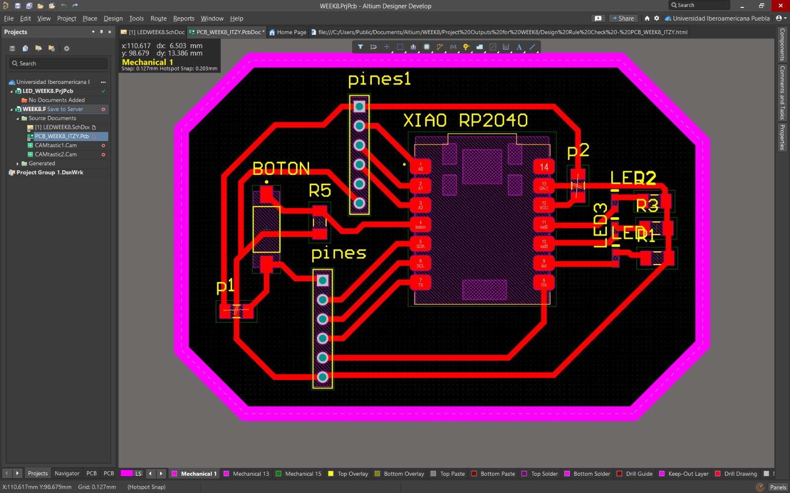
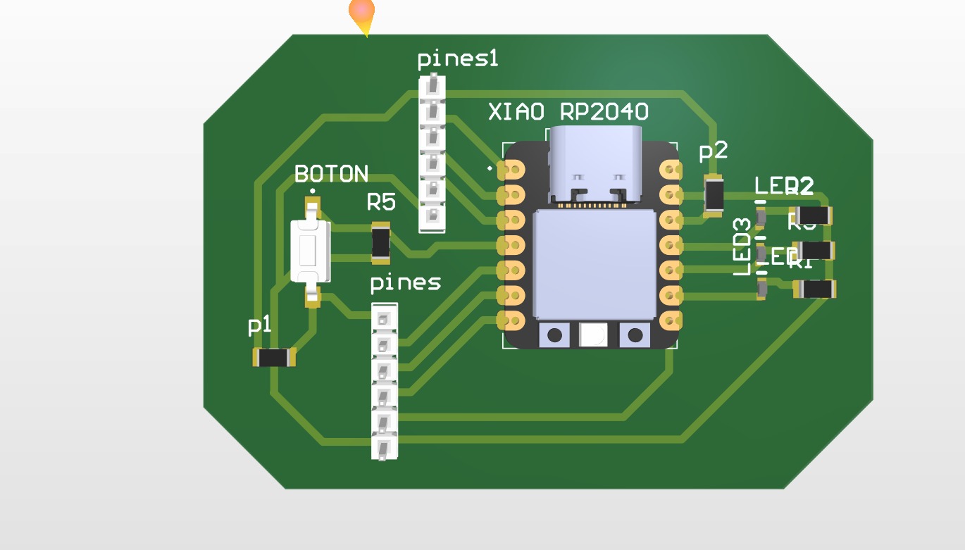
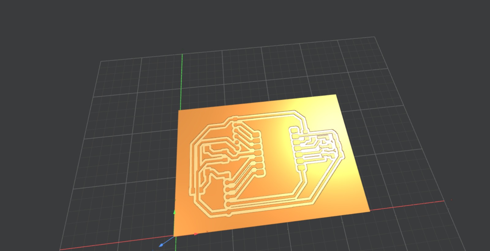
Once the circuit is established, it is transferred to PCB. From there, each component must be arranged. For this, I considered the input port of the microcontroller, as well as placing pins on the sides of the microcontroller to create simpler connections. Finally, I integrated the rest of the components according to spaces that were closer to their corresponding pins.
During this stage, I encountered a detail (easy to solve, fortunately!), in which I could not make connections between pins because they were enclosed by the traces. To solve this, I created a bridge with a zero-ohm resistor in those spaces where I could not complete the remaining connections.
A zero-ohm resistor is used to connect two traces that do not touch. It can be seen as a connecting wire.
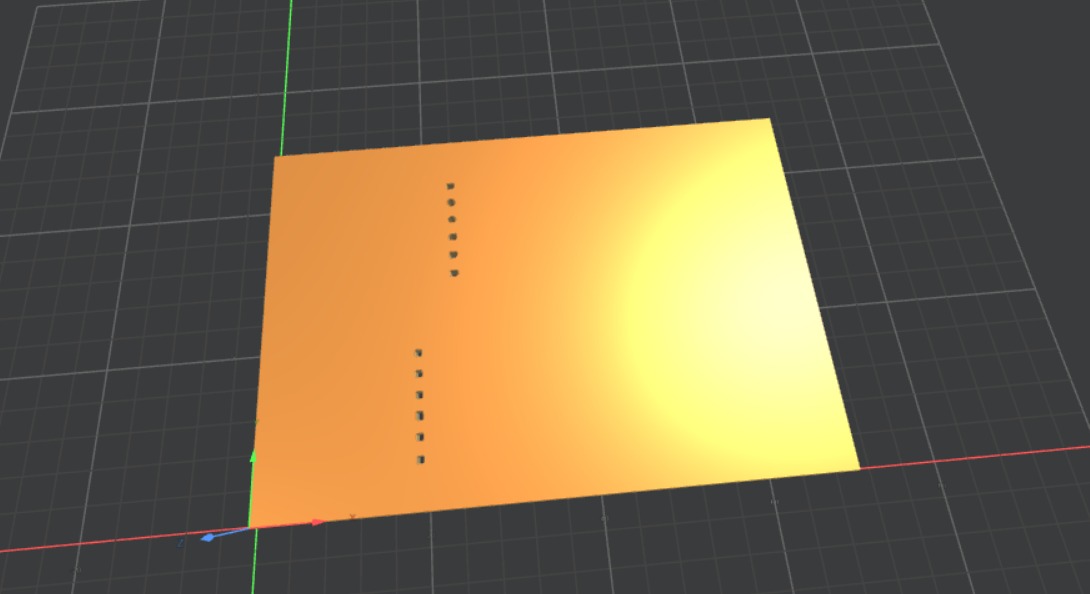
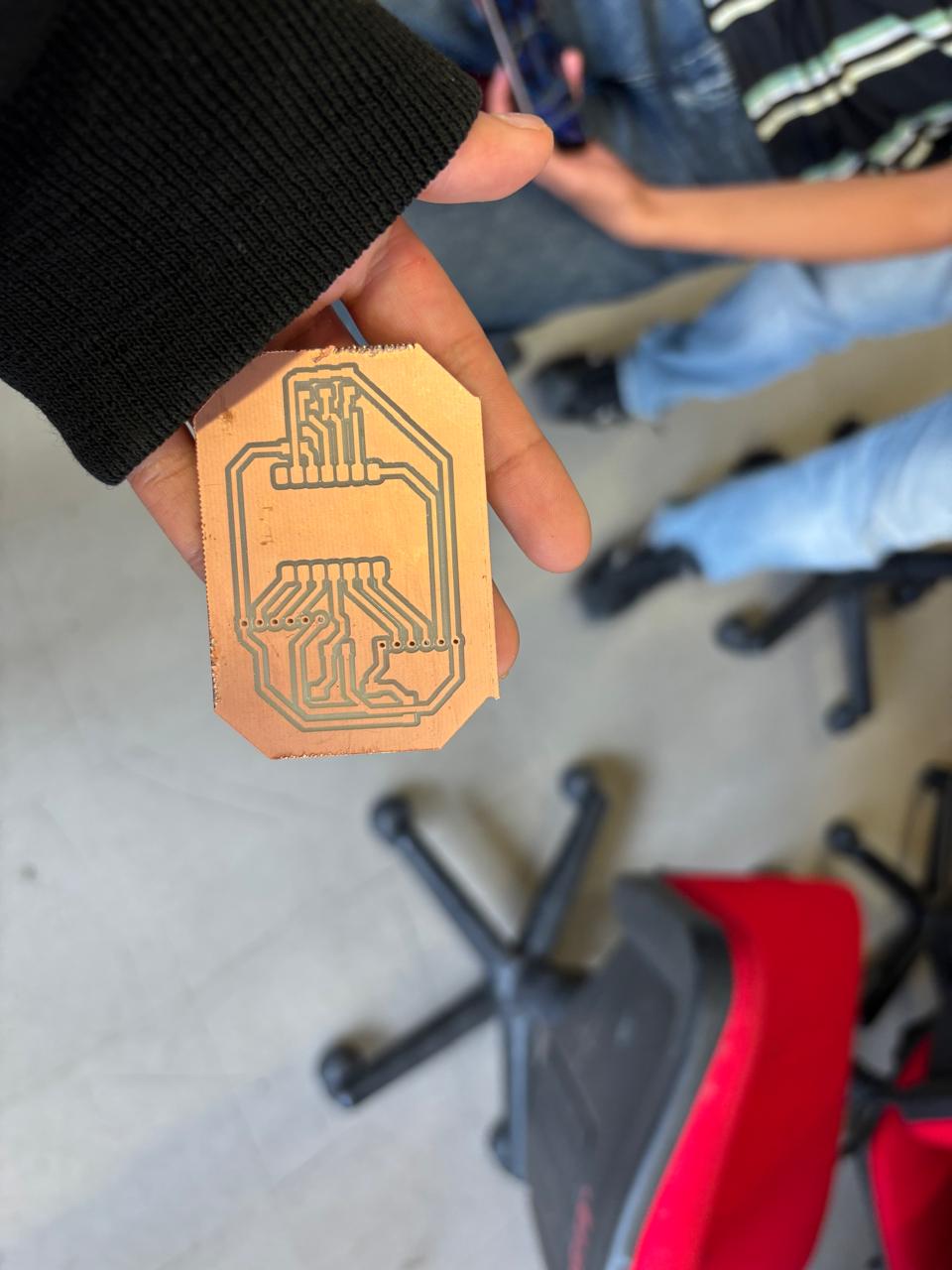
Once the components were arranged and wired, the shape of the board was defined.
To export my files to Gerber (files with specific information layer by layer establishing the traces present in the design), I followed these steps:
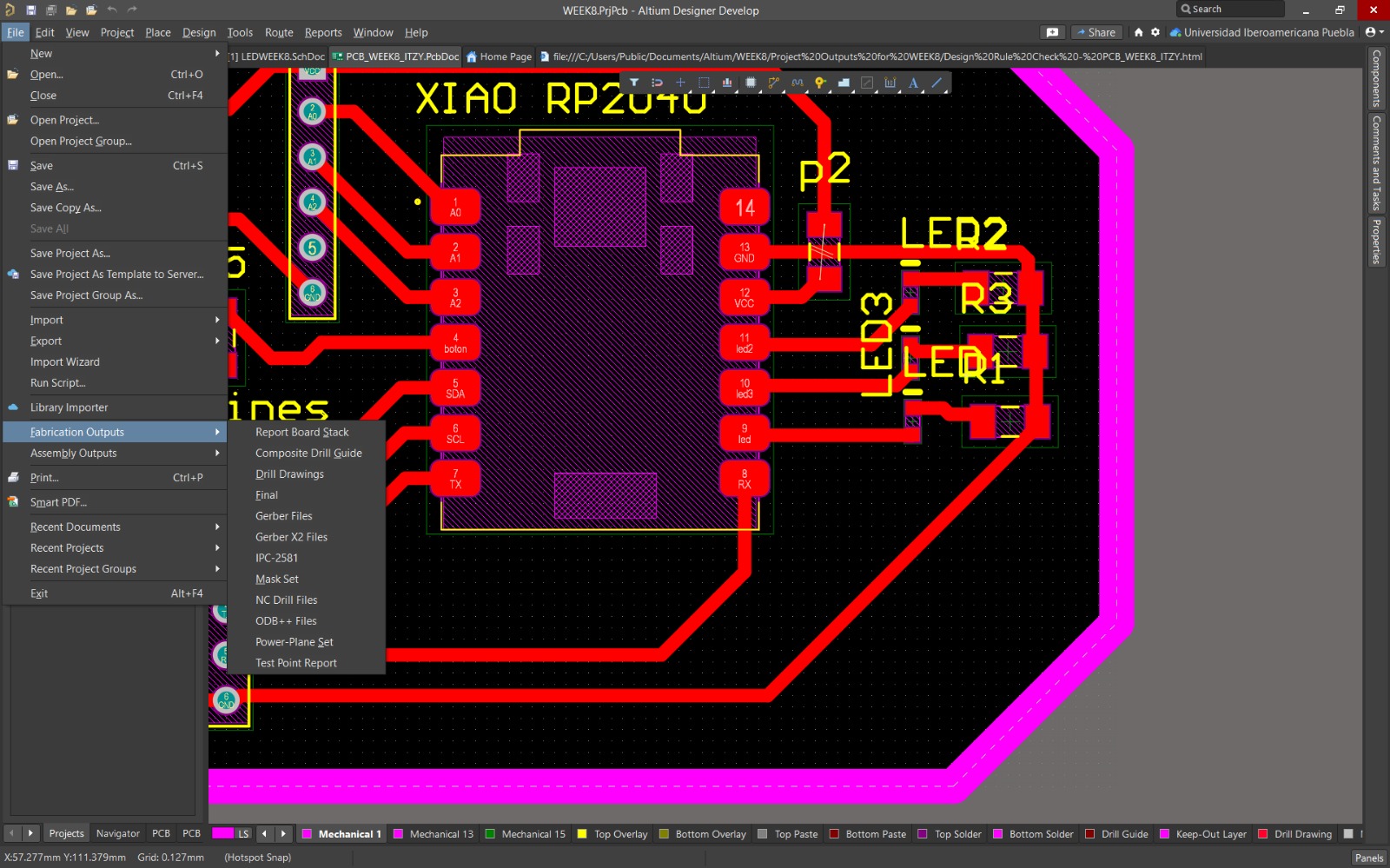
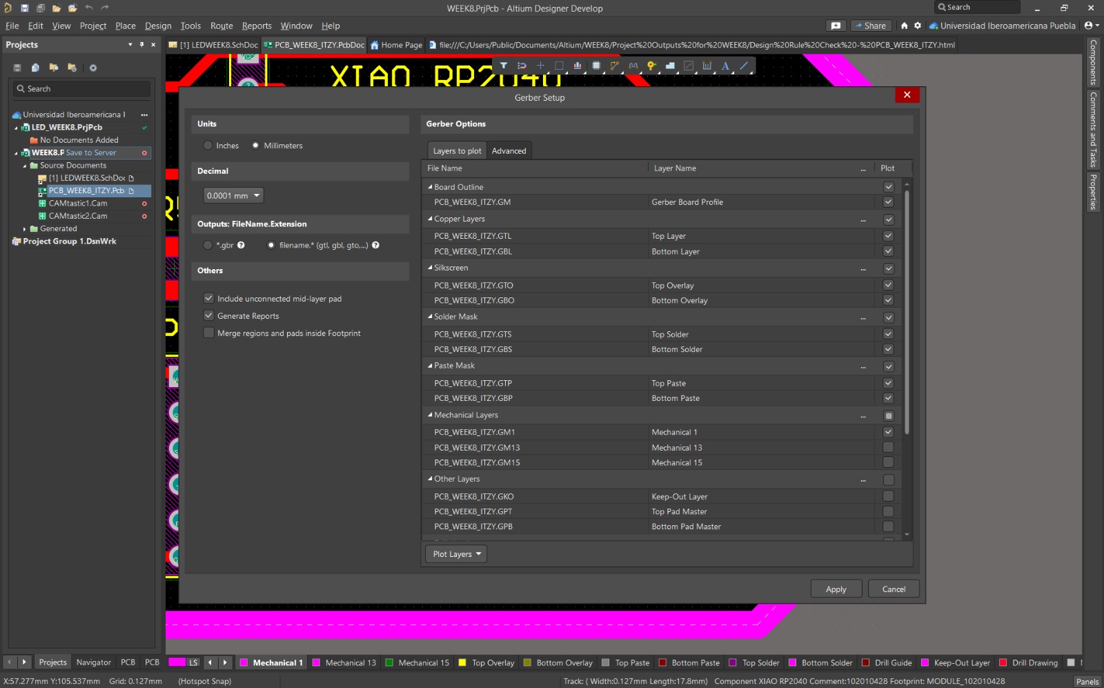
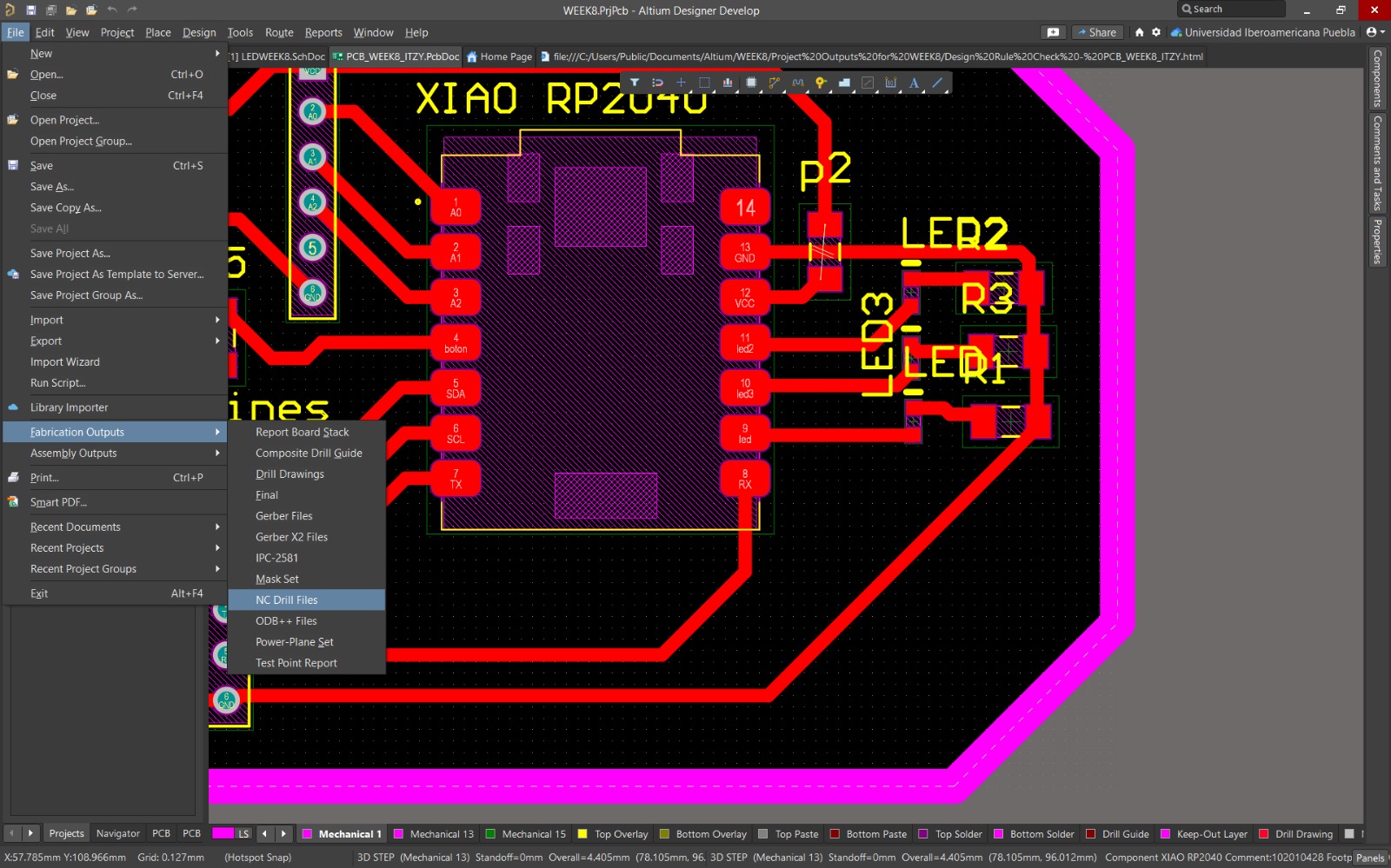
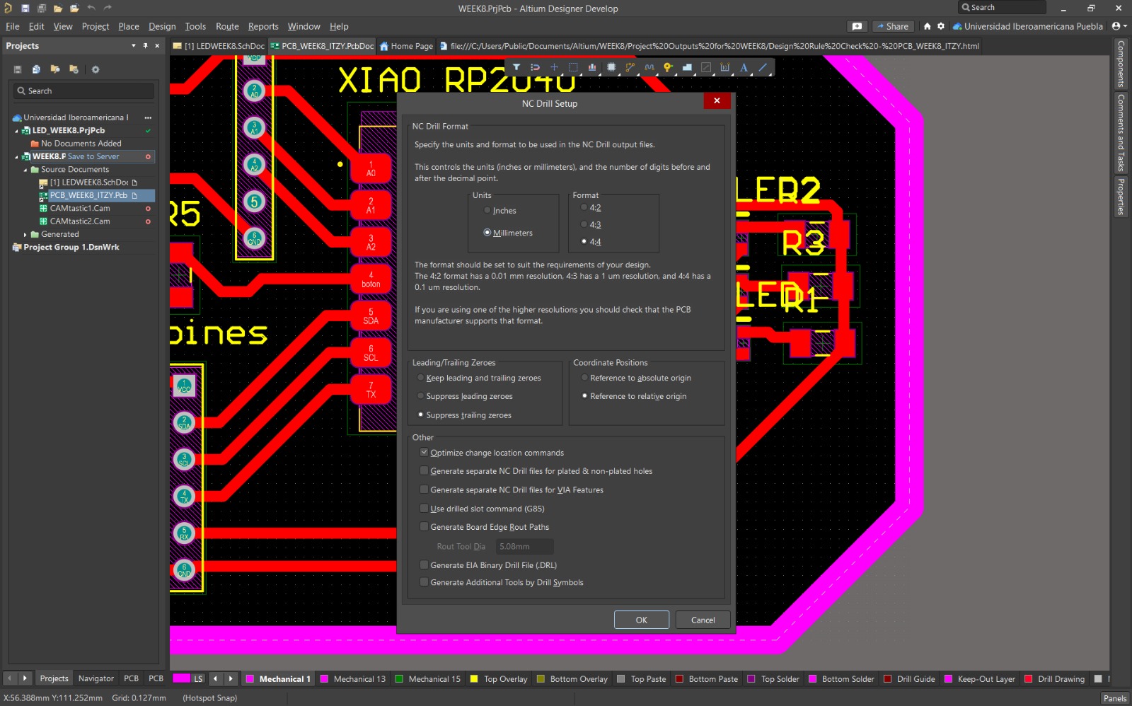
Once these steps are completed, Altium creates a folder where these files are saved, ready to continue with the next steps!
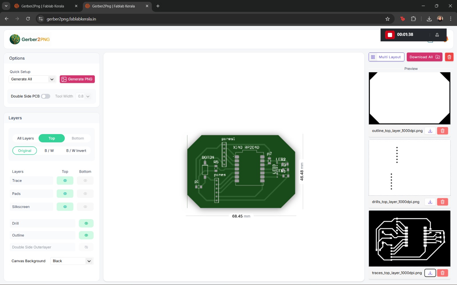
This step was very simple. I accessed the Gerber2png page. Then, from the folder generated by Altium, I selected the files and uploaded them. Immediately, in Quick Setup, the options Top Trace, Top Drill, and Top Cut appeared. I generated the images and then downloaded them. Done!
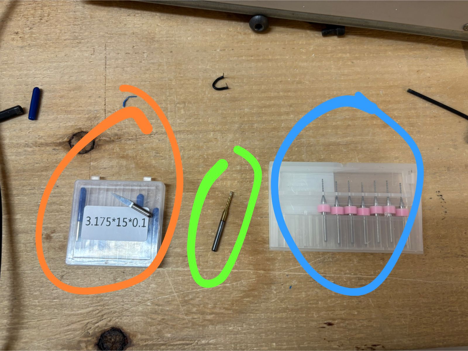
To configure the tool type, speed, and necessary parameters for cutting, I used Mods CE. In this, the required parameters for manufacturing can be defined.
I selected Drill; the general parameters appeared, from there I mainly changed the speed to 0.2 and the origins to 0.
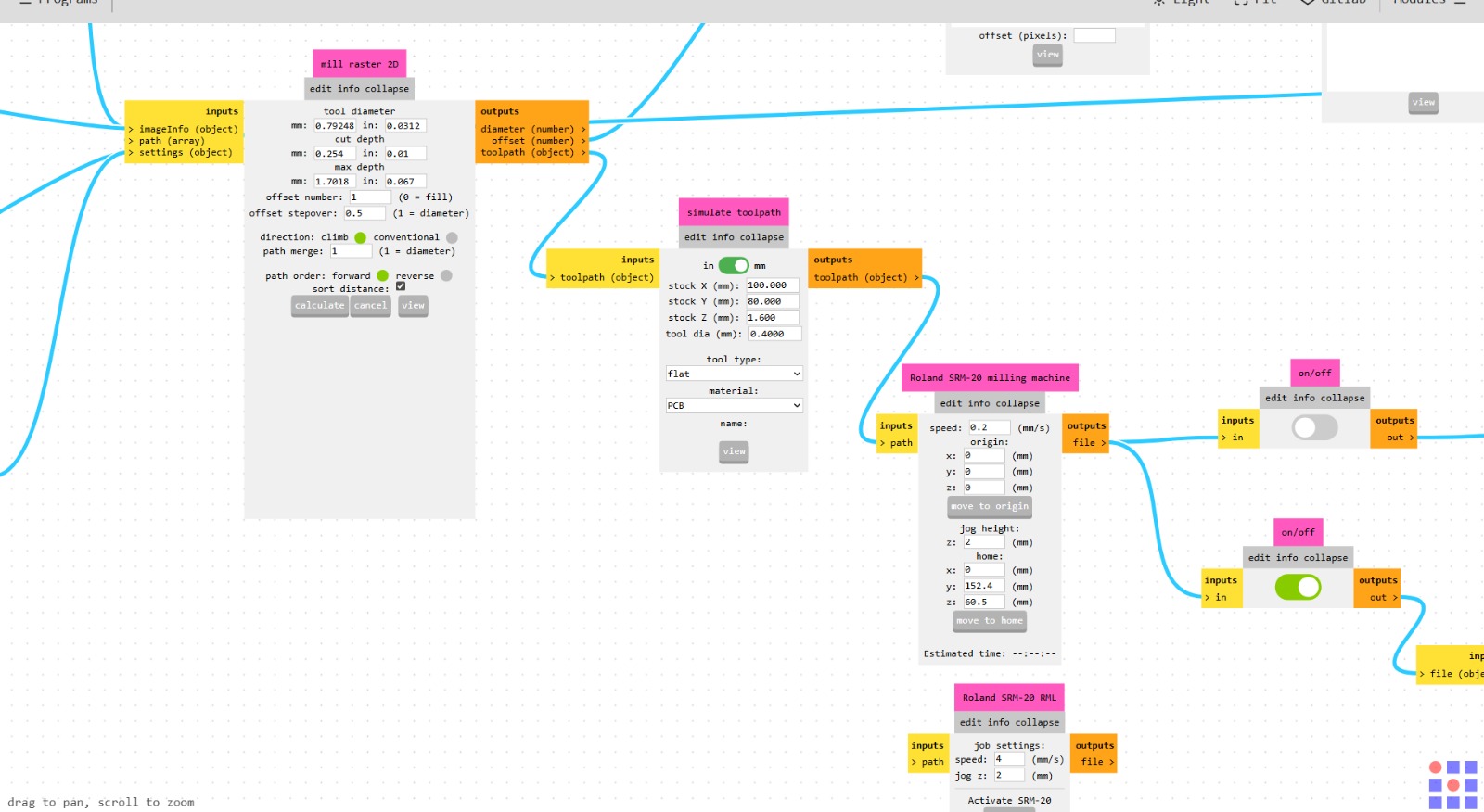
For engraving, these values are used. I also set Traces to 0.40 mm and adjusted the parameters accordingly.
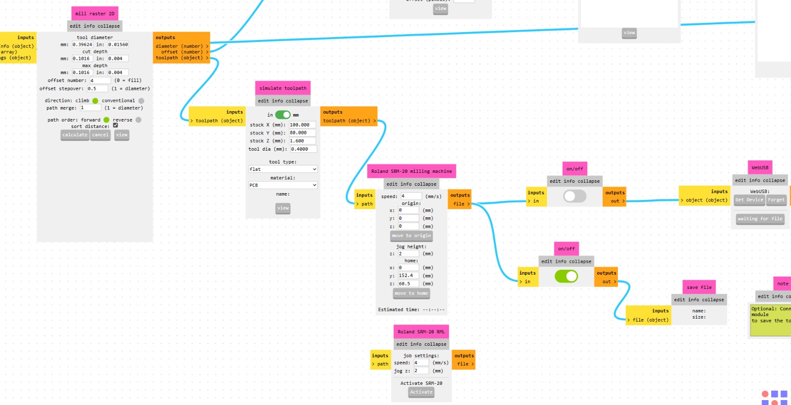
To finish and make the outline, I used Cutcut of 1.59 mm but changed the tool size to 2 mm.
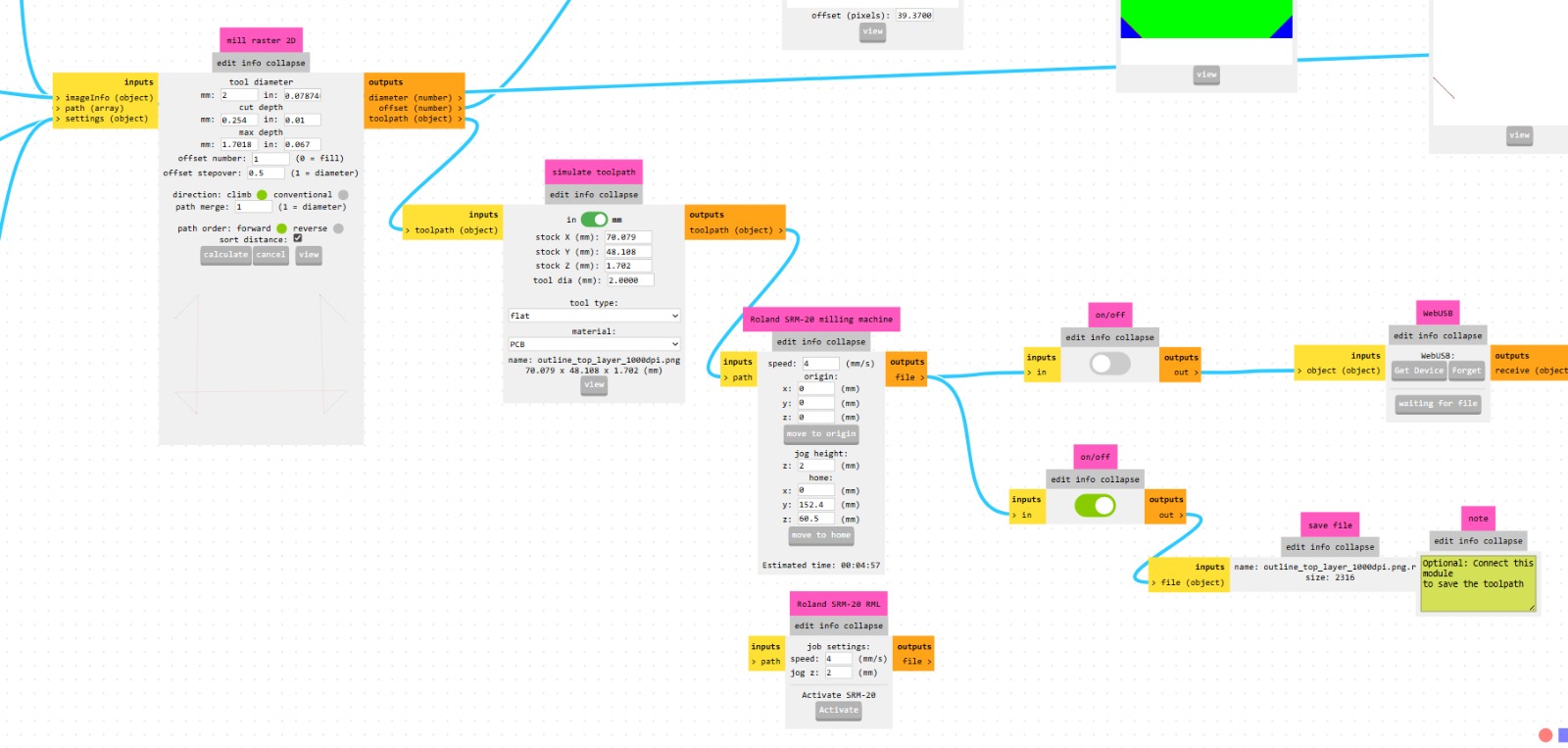
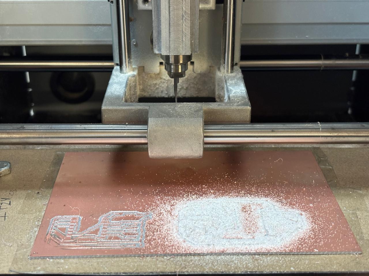
It is important to activate the files option so that the program that the CNC machine will follow is downloaded. At the same time, another window will open showing the simulations of each trace.
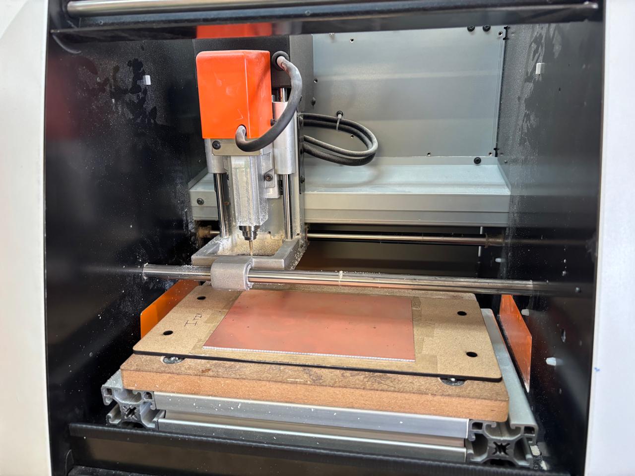
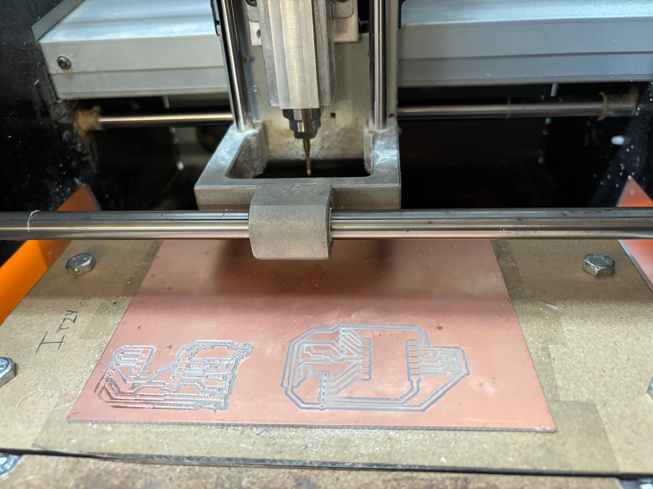
To manufacture the PCB board, an order is followed. First, the holes are made, then the traces, and finally the board is cut. In this way, the following steps were followed:
there is no specific technique that must be followed. However, I recommend soldering from the smallest components to the largest, to avoid collisions or limitations in the working area.
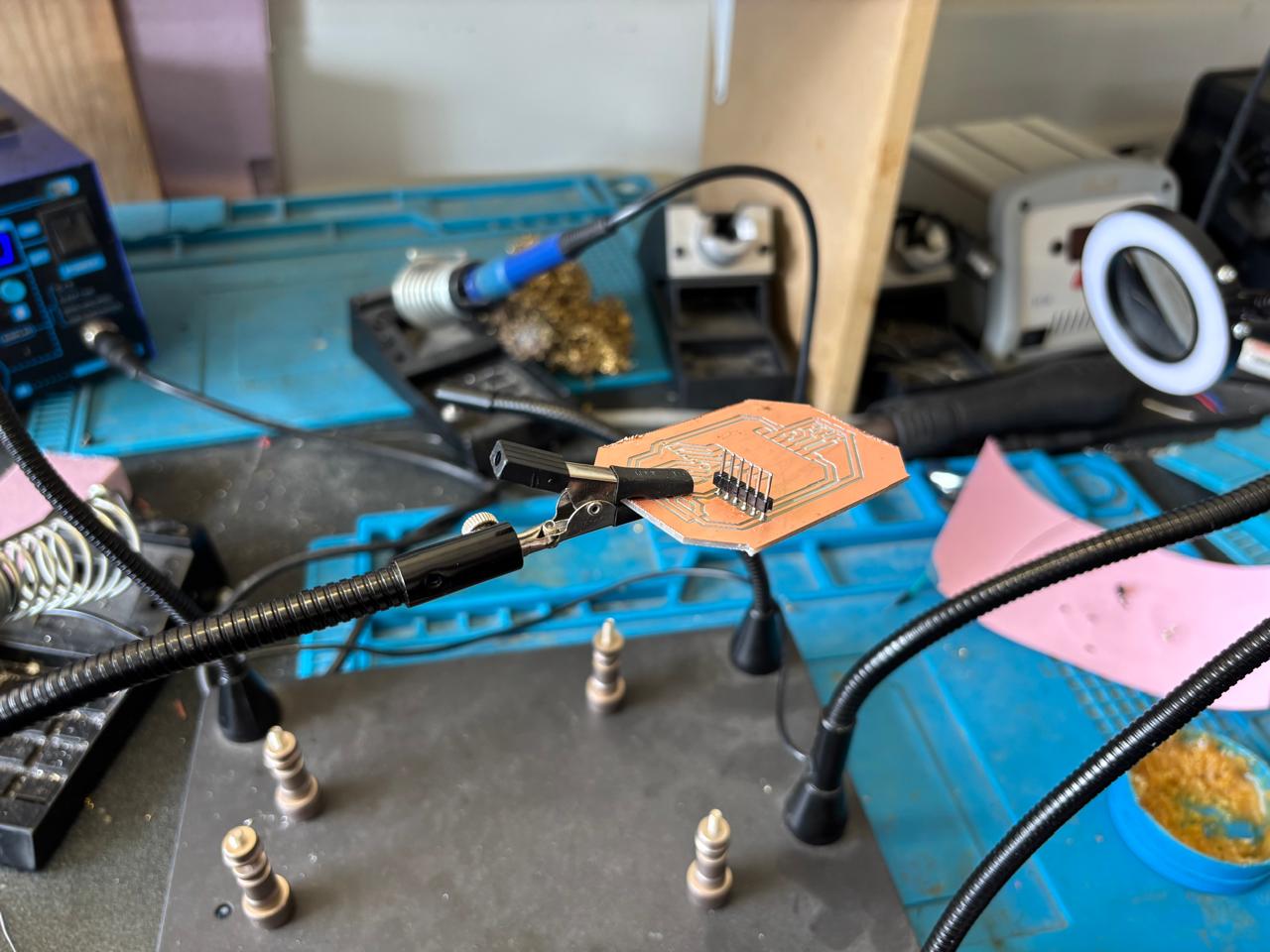
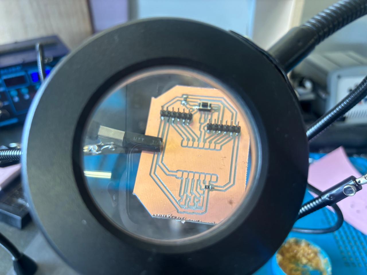
I used a bit of paste, placed it in the area to be soldered, and then used the soldering iron and solder to complete the joint. Regarding the soldering iron temperature, I allowed it to heat up to 270°. Usually, the range for soldering is between 290° and 300°, however, since it was my first time, I used a lower temperature.
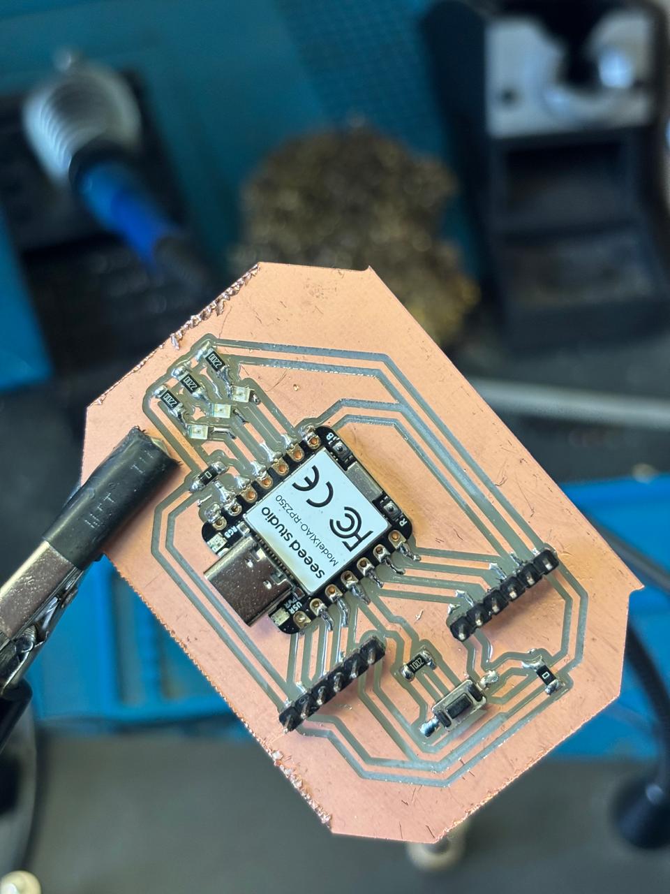
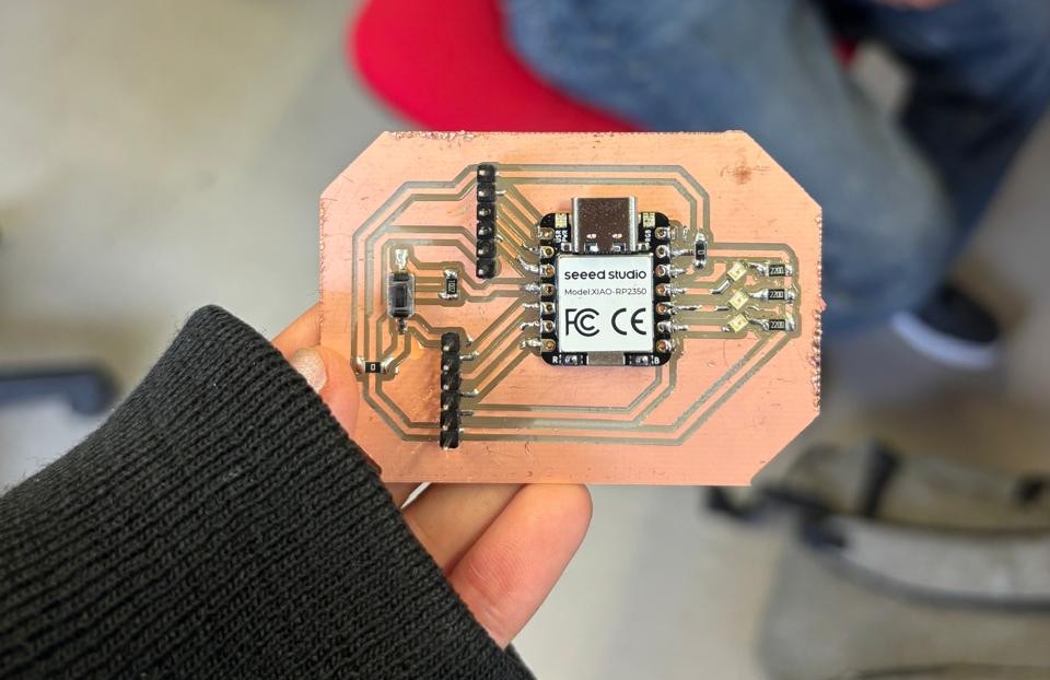
I soldered all my components. Once finished, I used a voltmeter to check that no connections were made between traces.
Once the board was finished, I connected the microcontroller to my laptop using a Type-C cable. To program the board, I downloaded Arduino IDE. Then, I added the library for this type of board.
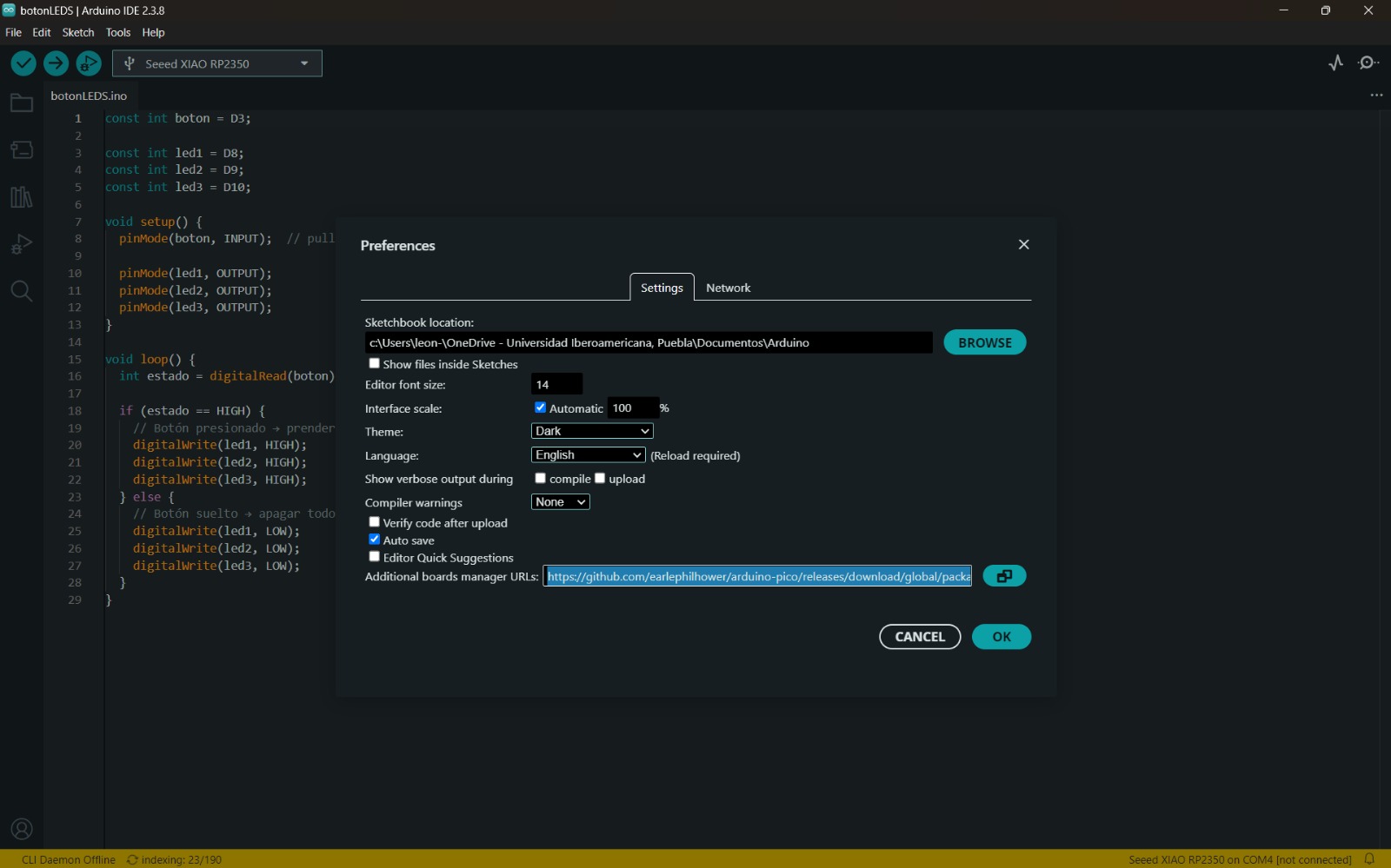
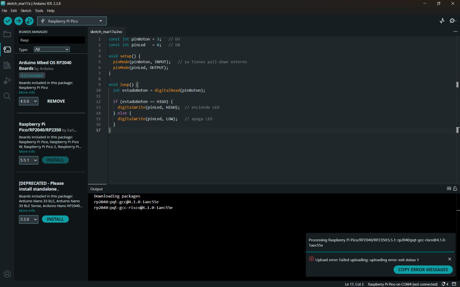
Finally, I performed a very simple test where I turned on the three LEDs to verify that everything worked correctly, and another test where the button could be used to turn them on. The codes used were:
                    void setup() {
                        pinMode(D8, OUTPUT);
                        pinMode(D9, OUTPUT);
                        pinMode(D10, OUTPUT);
                    }

                    void loop() {
                        // Encender todos
                        digitalWrite(D8, HIGH);
                        digitalWrite(D9, HIGH);
                        digitalWrite(D10, HIGH);
                        delay(1000);

                    // Apagar todos
                        digitalWrite(D8, LOW);
                        digitalWrite(D9, LOW);
                        digitalWrite(D10, LOW);
                        delay(1000);
                    }
                    const int boton = D3;
                    const int led1 = D8;
                    const int led2 = D9;
                    const int led3 = D10;

                    void setup() {
                      pinMode(boton, INPUT);

                      pinMode(led1, OUTPUT);
                      pinMode(led2, OUTPUT);
                      pinMode(led3, OUTPUT);
                    }

                    void loop() {
                      int estado = digitalRead(boton);

                      if (estado == HIGH) {
                      // Botón presionado → prender todos
                      digitalWrite(led1, HIGH);
                      digitalWrite(led2, HIGH);
                      digitalWrite(led3, HIGH);
                    } else {
                      // Botón suelto → apagar todos
                      digitalWrite(led1, LOW);
                      digitalWrite(led2, LOW);
                      digitalWrite(led3, LOW);
                    }
                }
In this way, I managed to manufacture a PCB board using a XIAO RP2350 microcontroller.
It is necessary to understand the operation of the design of an electronic system, since this is basically the brain of many projects. For me, it was important to learn and manufacture a PCB board, since acquiring this knowledge is enriching. PCB boards are extremely necessary for current technologies. Therefore, without a doubt, this week allowed me to learn how to manufacture boards and not only stay at their design, since these are skills that I will apply in the future for the construction of my final project.
If you want to access to my work from this week, please click here to download!
Finally, for the group assignment for this week, you can find the information here