Use the test equipment in your lab to observe the operation of a microcontroller circuit board (as a minimum, you should demonstrate the use of a logic analyzer)
Document your work on the group work page and reflect what you learned on your individual page
Individual assignments
Use an EDA tool to design a development board that uses parts from the inventory to interact and communicate with an embedded microcontroller
What is Electronics Design?
Electronics design is the process of creating and developing electronic circuits or systems. It is widely applied in different areas of technology. It is necessary to understand the fundamentals of electronics, the function of electronic components, and their operating principles. Particularly for this week, the objective is to design a printed circuit board (PCB).
The design must go through verification and simulation stages, which help guarantee the reliability of the board. Likewise, it is necessary to understand and comply with design standards.
Fundamentals of Electronics
There are fundamental principles that must be considered when designing a circuit. For me, it was also important to become familiar with the electronic components that are most frequently used. It is necessary to understand Ohm’s Law, electric power, circuit analysis, and related concepts.
Regarding components, the most commonly used ones include resistors, which are used to limit electric current; capacitors, which store electric charge; diodes, which allow current to flow in one direction; and transistors, which act as switches.
What programs can you use?
There are several programs that can be used for circuit design. I mainly used two programs that I found intuitive, easy to use, and simple to understand. Since I had never had any previous experience designing circuits or PCB boards, it was challenging for me to adapt to these software tools. However, I consider both KiCAD and Altium to have interfaces that are easy to understand.
KiCAD
KiCAD is open-source software for electronic design automation. It allows users to create electrical schematics, printed circuit boards, and more. It can be installed on Windows, Linux, and macOS.
It includes a schematic editor, PCB editor, and 3D viewer. It also allows multilayer designs, design rule verification, and simulation.
How to Use KiCAD
Schematic Design
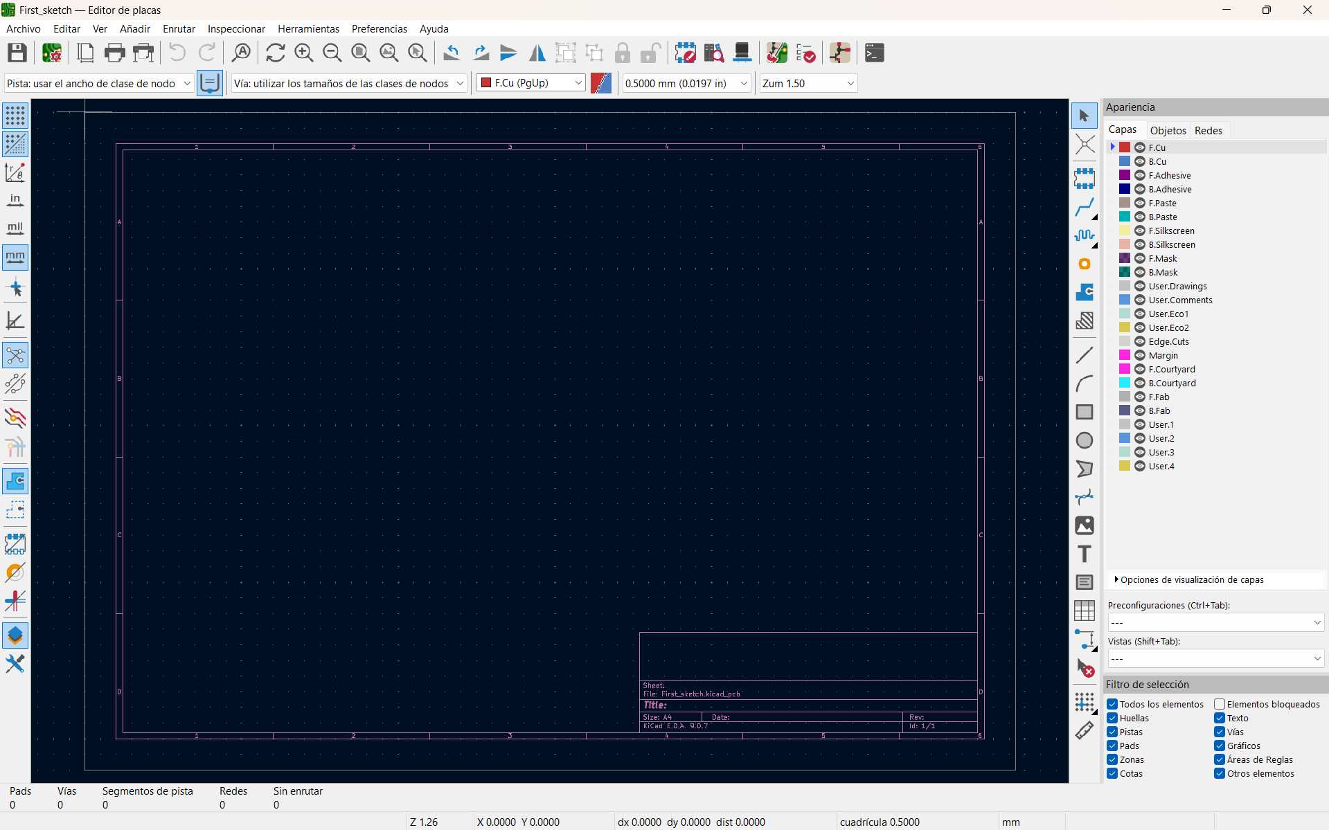
KiCAD is a free program, so you can download it from its official website. After downloading and installing it, when you open the program, you will see the main interface. It provides a wide variety of tools such as the Schematic Editor, Symbol Editor, PCB Editor, and calculation tools.
To begin the schematic design, select File → New Project. This option will open a window where you can save your project. Once you assign a name, the program will generate two files: one for the schematic (saved in .sch format) and another for the PCB (saved in .pcb format). Select the .sch file.
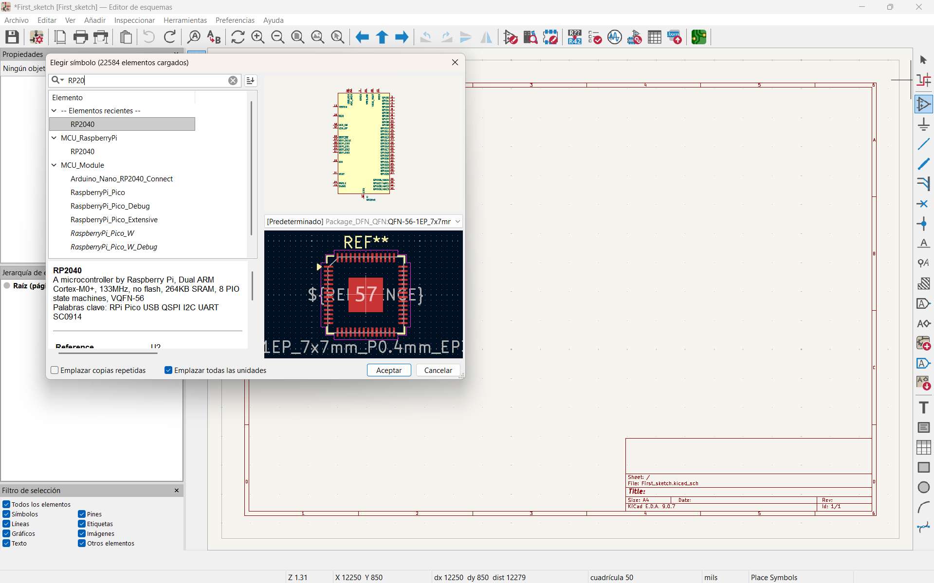
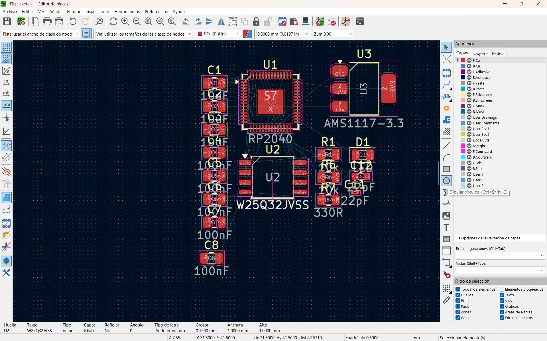
To add components, you can search for them using the symbol that looks like a triangle located on the right toolbar. In my case, I searched for an RP2040 microcontroller.
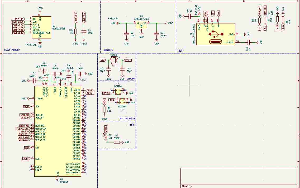
Then, I continued adding components according to my circuit design.
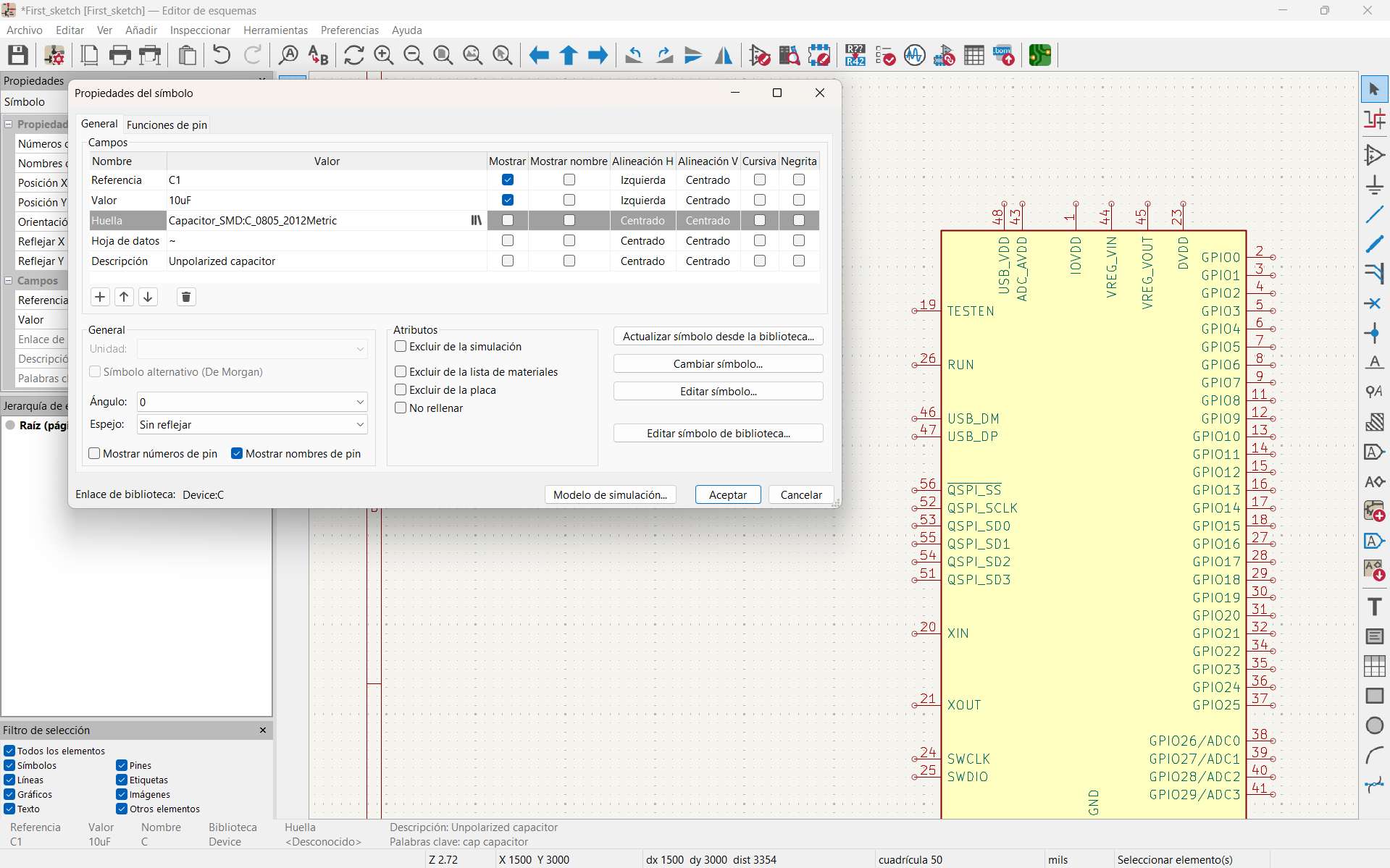
To assign footprints to the components, open the symbol properties (double-click on the component). In the footprint section, a symbol will allow you to search for footprints that KiCAD provides automatically.
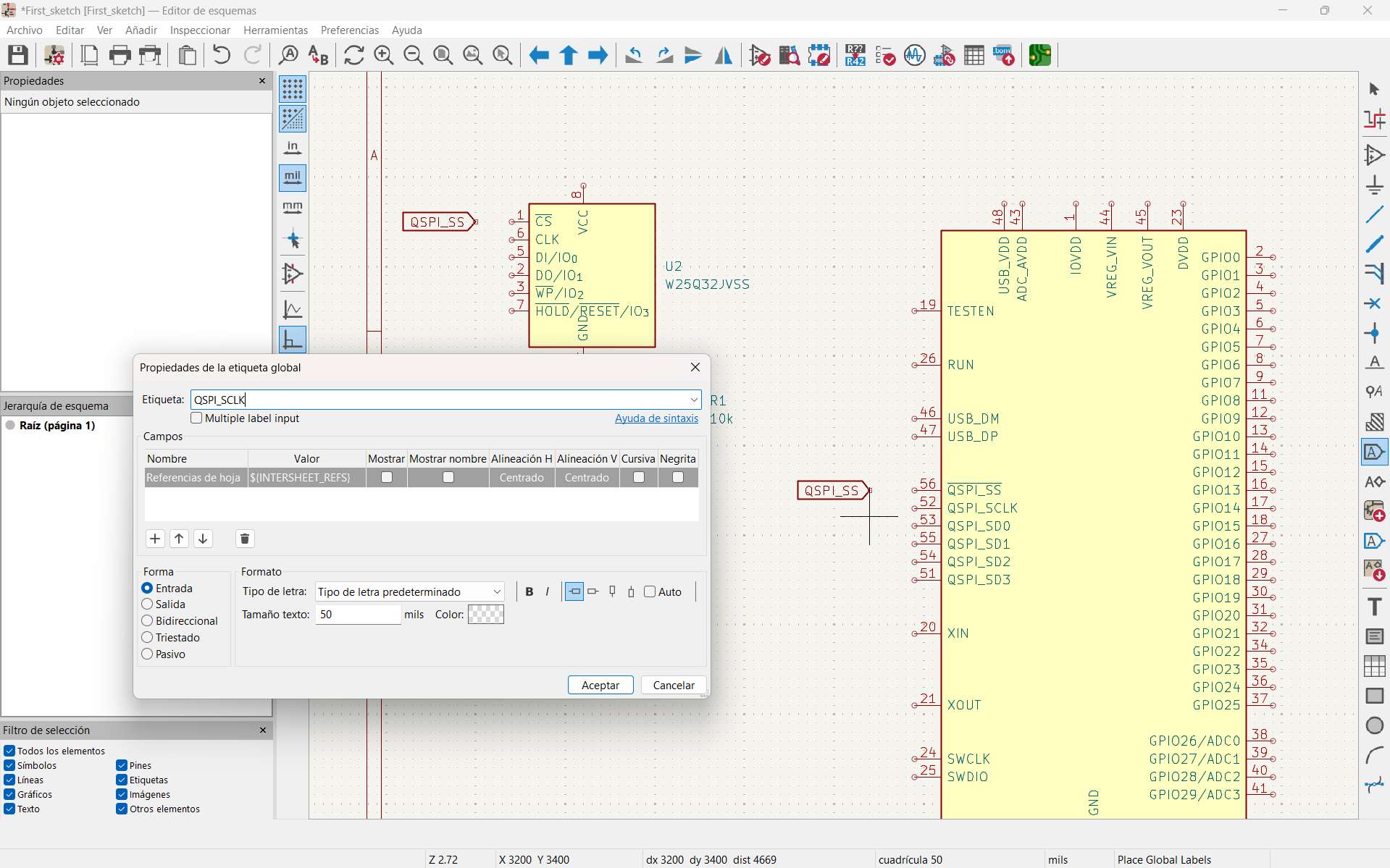
Components can be connected in two ways. The first is by directly drawing wires (press W). The second is by adding labels. Labels can be placed using Ctrl + L or by selecting the symbol with the letter “A.” For connections to work correctly, the connection names must be exactly the same.
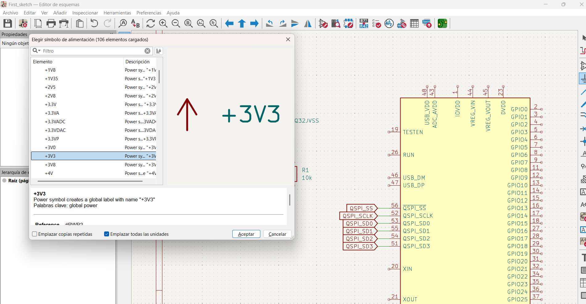
To add power symbols, press the letter P. A window will automatically open where you can select and place the corresponding power symbols.
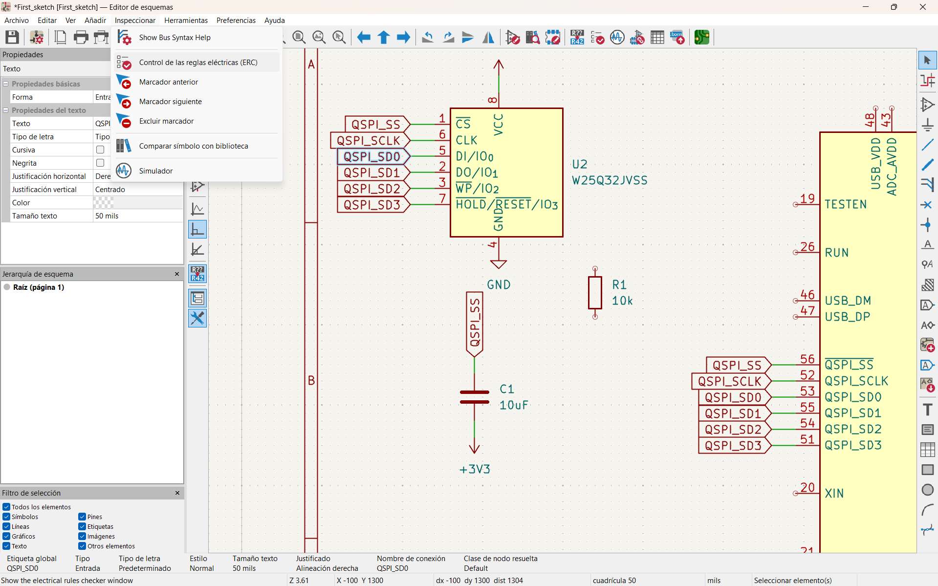
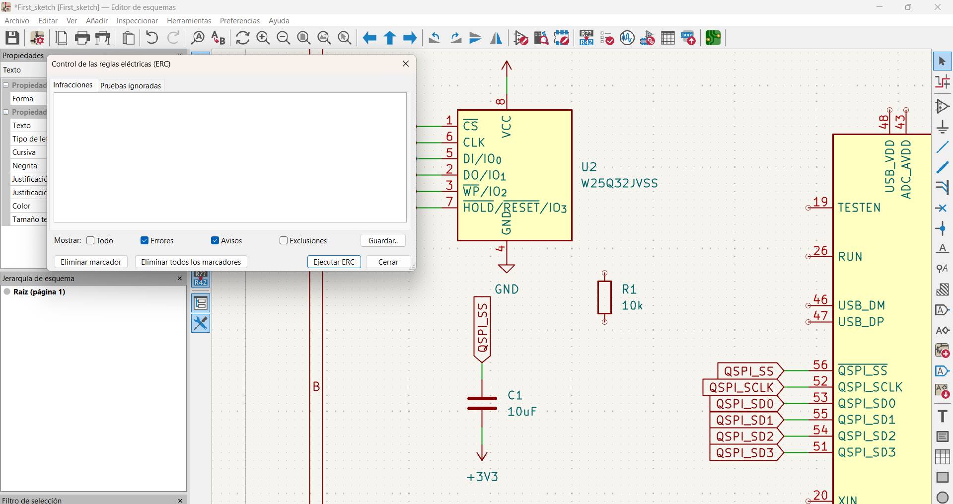
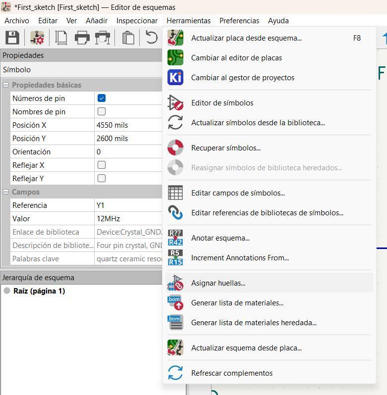
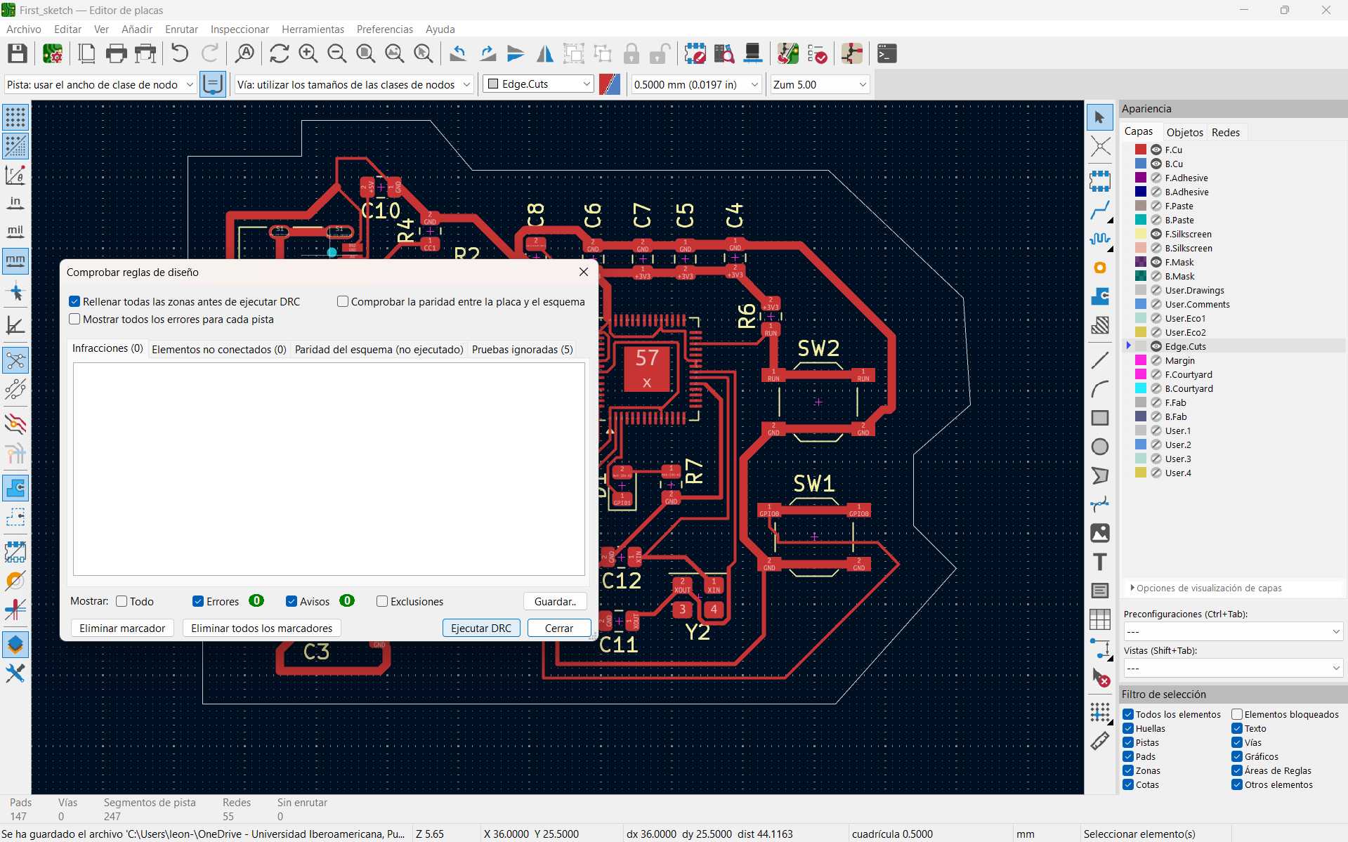
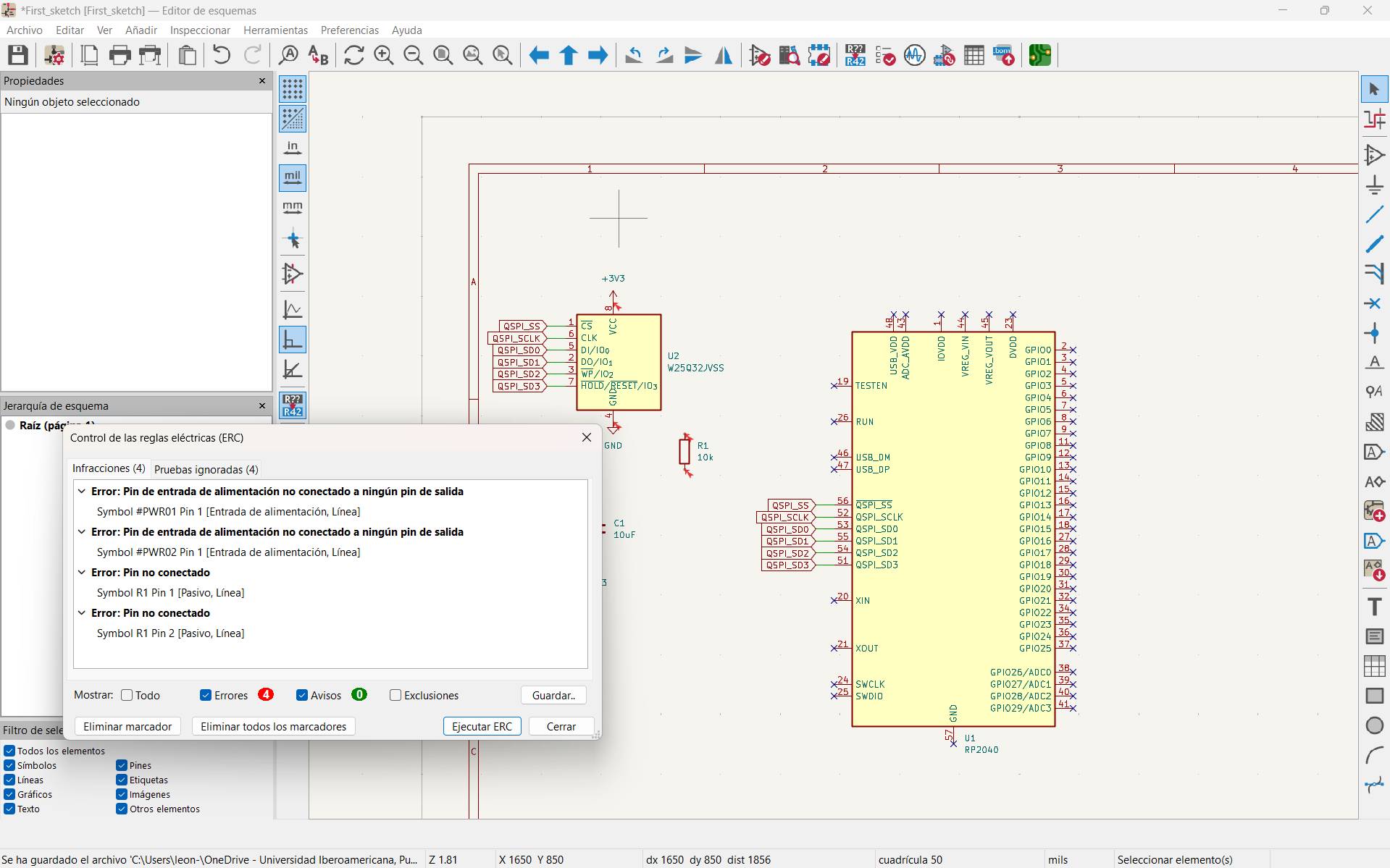
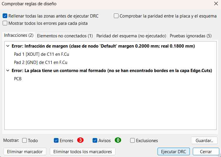
Once you finish assembling your circuit, you must verify that the rules are properly satisfied. To do this, select Inspect → Electrical Rules Checker (ERC) → Run ERC. Errors in your circuit will appear here so you can correct them before moving on to the PCB stage.
PCB Design
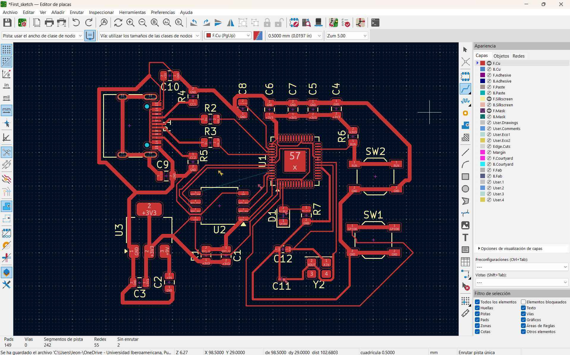
Once the circuit is complete, select Tools → Switch to PCB Editor. This will automatically open the PCB file.
To import the components, press F8 or go to Tools → Update PCB from Schematic. A window will open. Select the parameters you consider appropriate, accept, and close the window. Your components will immediately appear.
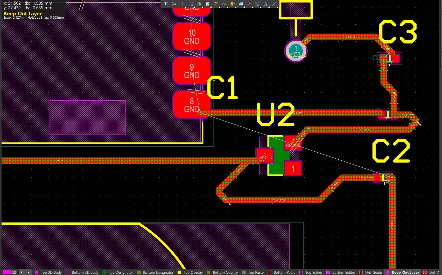
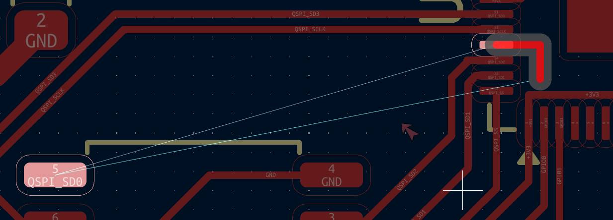
Begin by organizing your components. Once arranged, start routing the connections. Usually, the program indicates which components must be connected by showing lines between them.
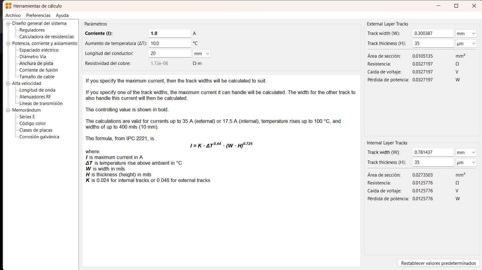
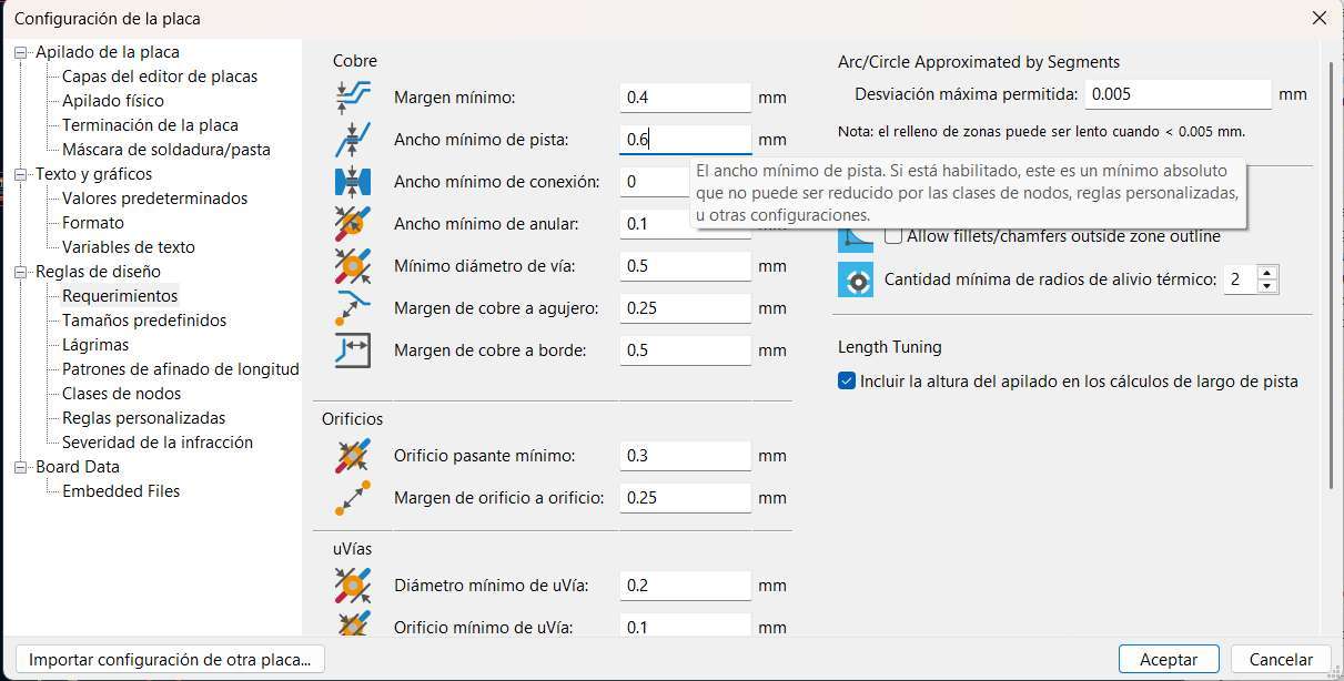
To determine the minimum trace width required, you can use KiCAD’s calculator. Go to Power, Current and Isolation → Track Width. There, you can enter the current your circuit will carry and the allowed temperature rise. On the right side, the minimum required trace width will be displayed.
To modify the trace width, go to Board Setup → Design Rules → Constraints. Here, you can modify the minimum clearance and minimum track width according to your needs.
After finishing the routing, use the Draw Polygons tool (Ctrl + Shift + P) to draw the board outline and define its limits.
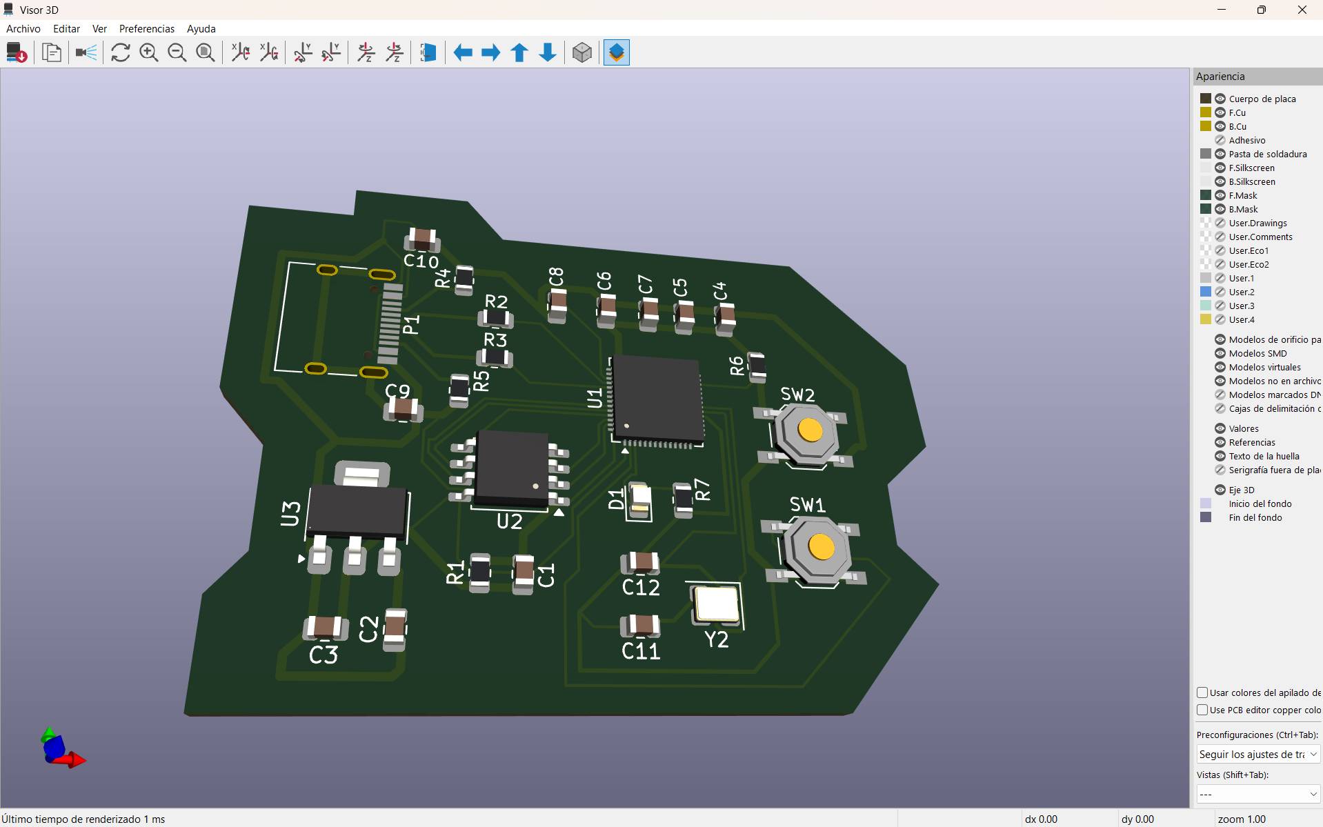
To visualize the board in 3D, select View → 3D Viewer or press Alt + 3.
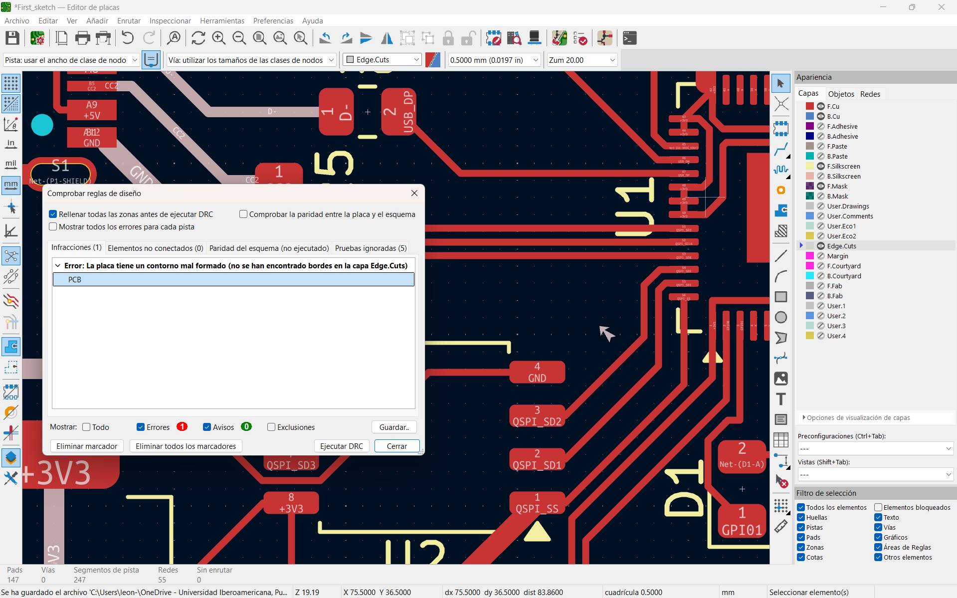
Finally, run the design rule check again to ensure everything is correct.
Altium
Like KiCAD, Altium is a program used for professional printed circuit board design. It allows the creation of schematics, circuit simulations, PCB layouts, and more. It requires a license to use.
How to Use Altium
Schematic Design
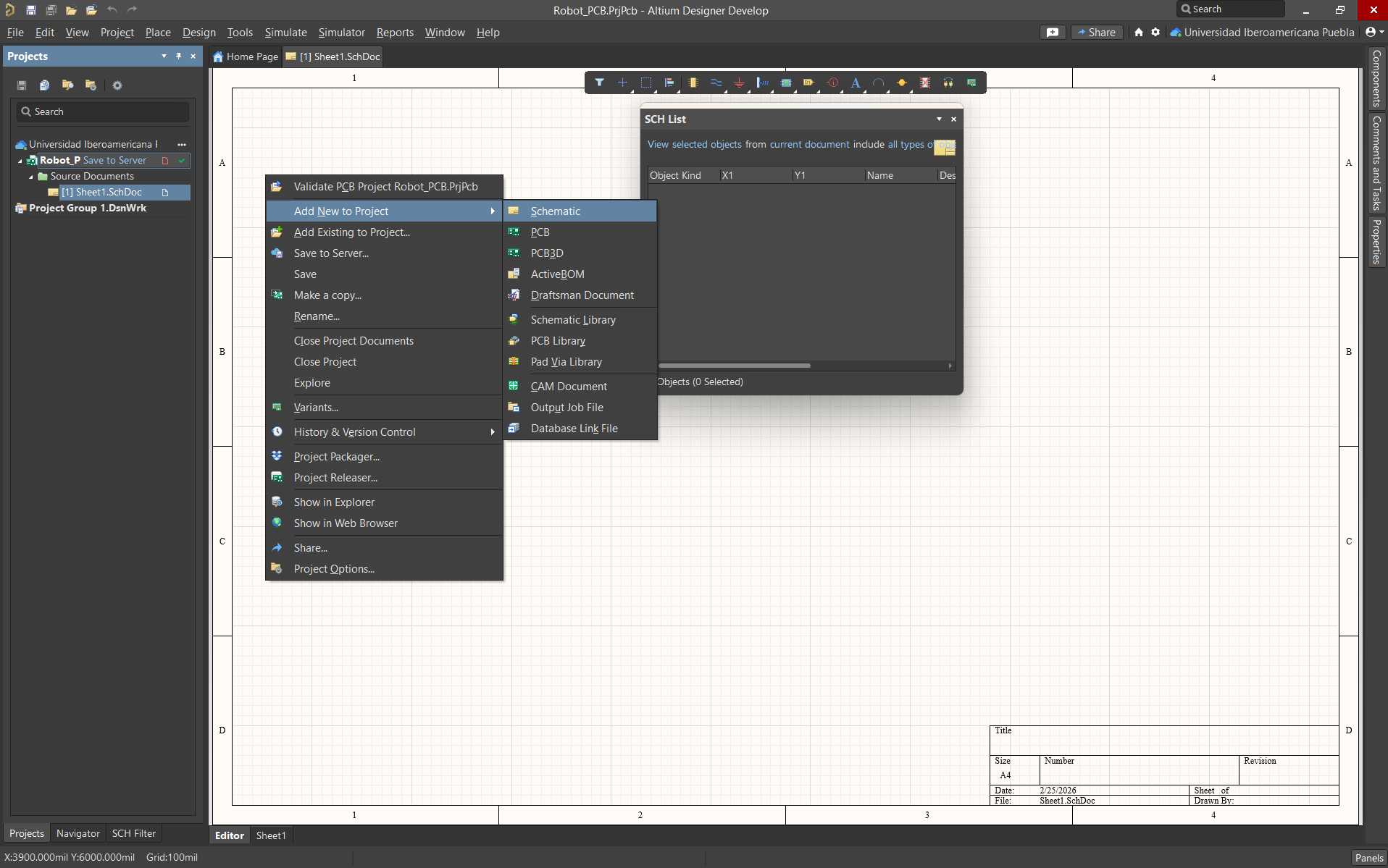
Open the program. You will start at the welcome interface. To create a new project, select File → New → Project.
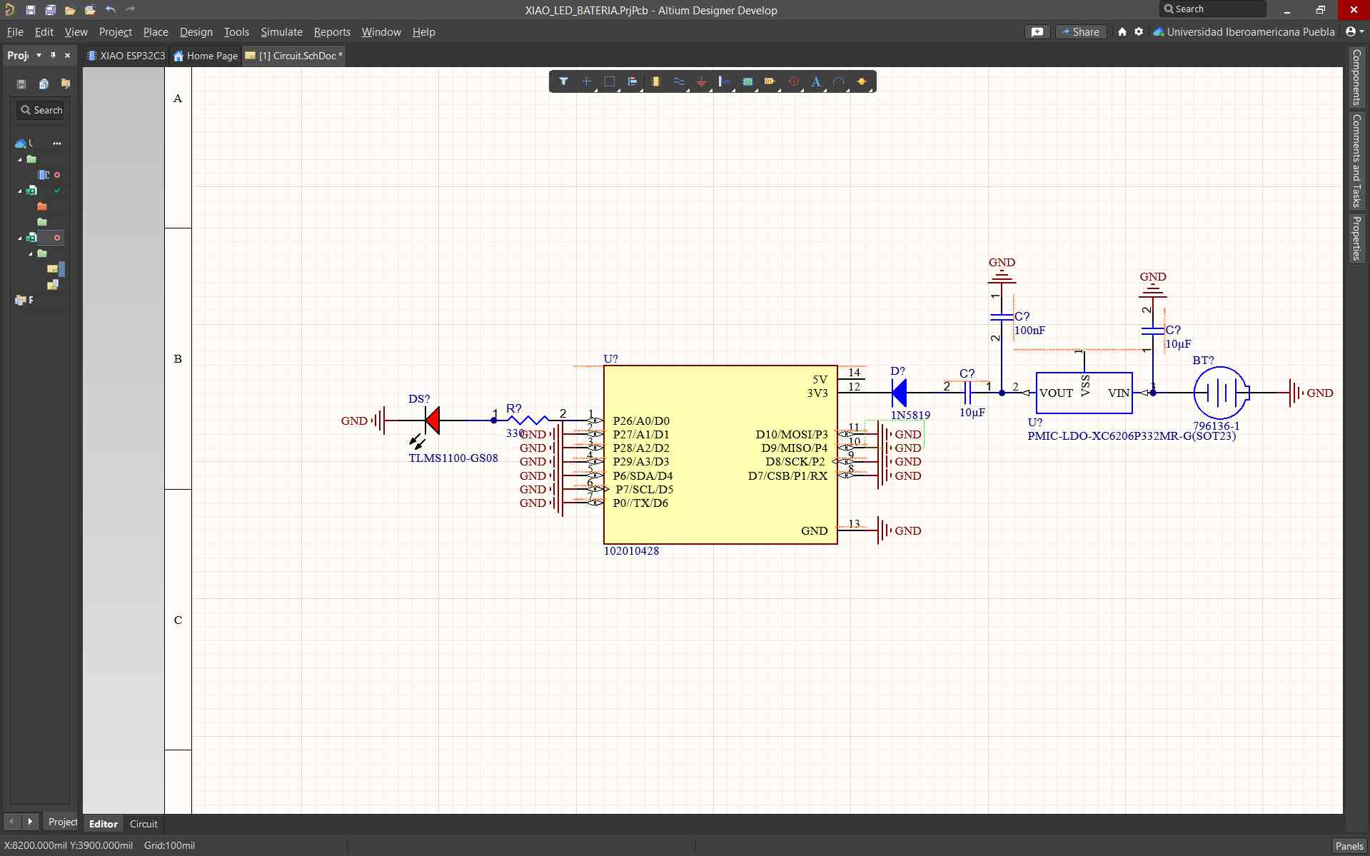
Once the project is saved, right-click on the project name. A list of options will appear. First, you need to create a schematic where the main circuit drawings are made. Select Right-click → Add New to Project → Schematic. A new schematic sheet will open.
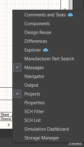
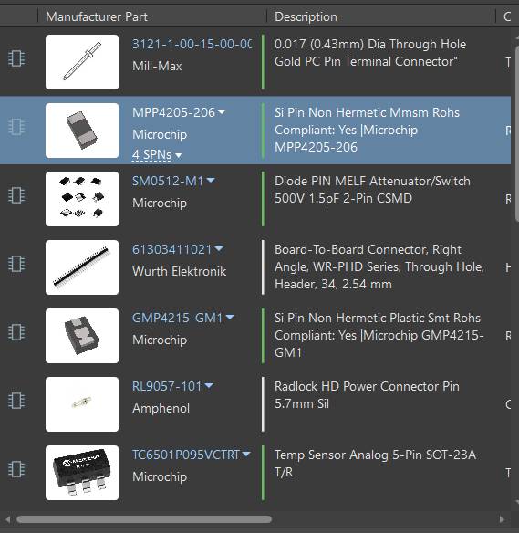
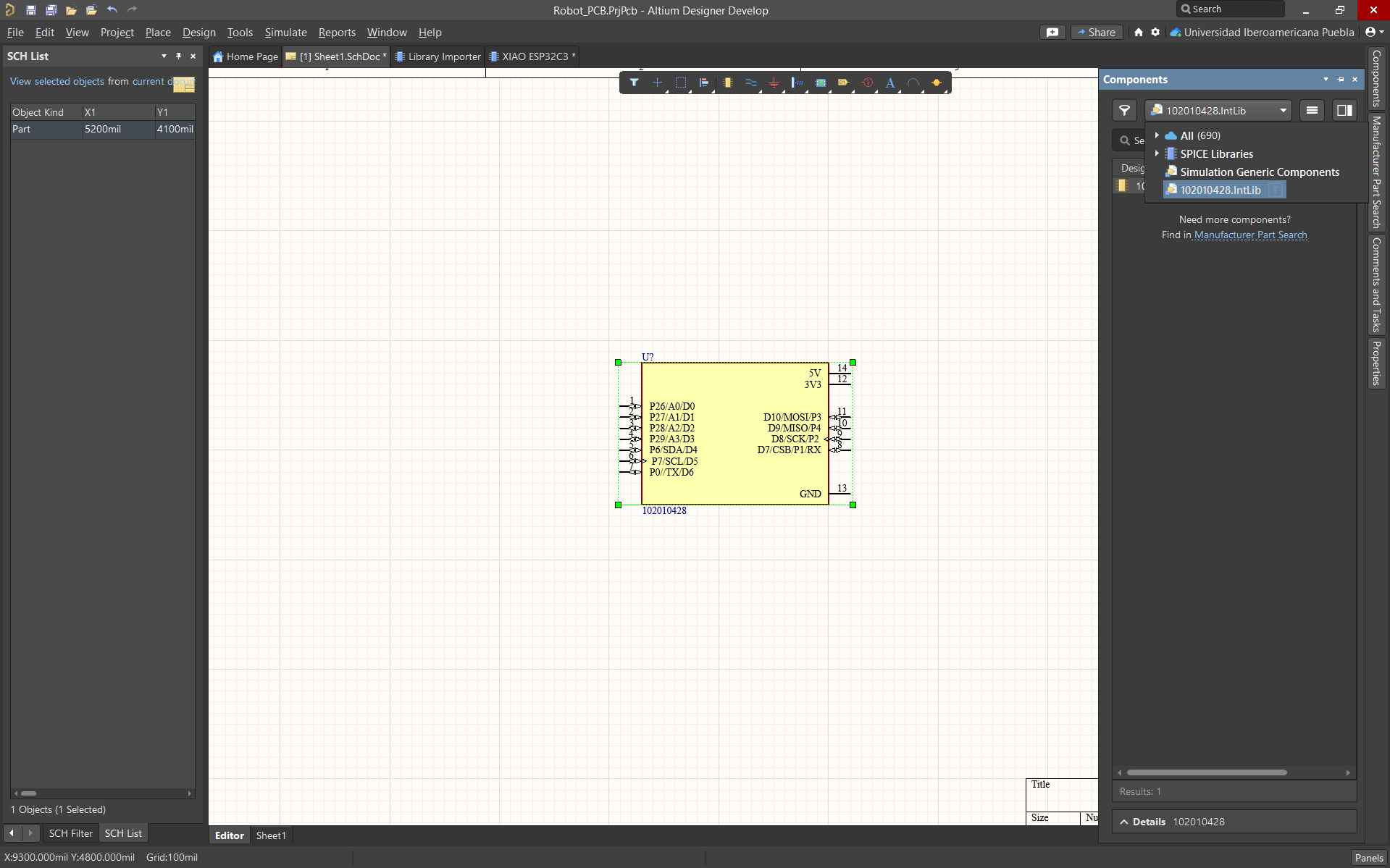
In the lower right corner, there is a Panels tab. This allows you to activate additional windows while drawing. For me, it was important to activate Components and Manufacturer Part Search, since I use them frequently to search for and add components to my schematic.
Before creating my schematic, it was important for me to define the list of components I would use and determine their function. This made it easier to understand their use and application in the circuit.
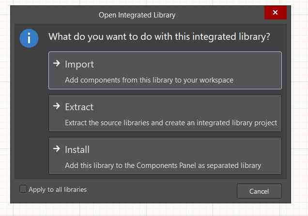
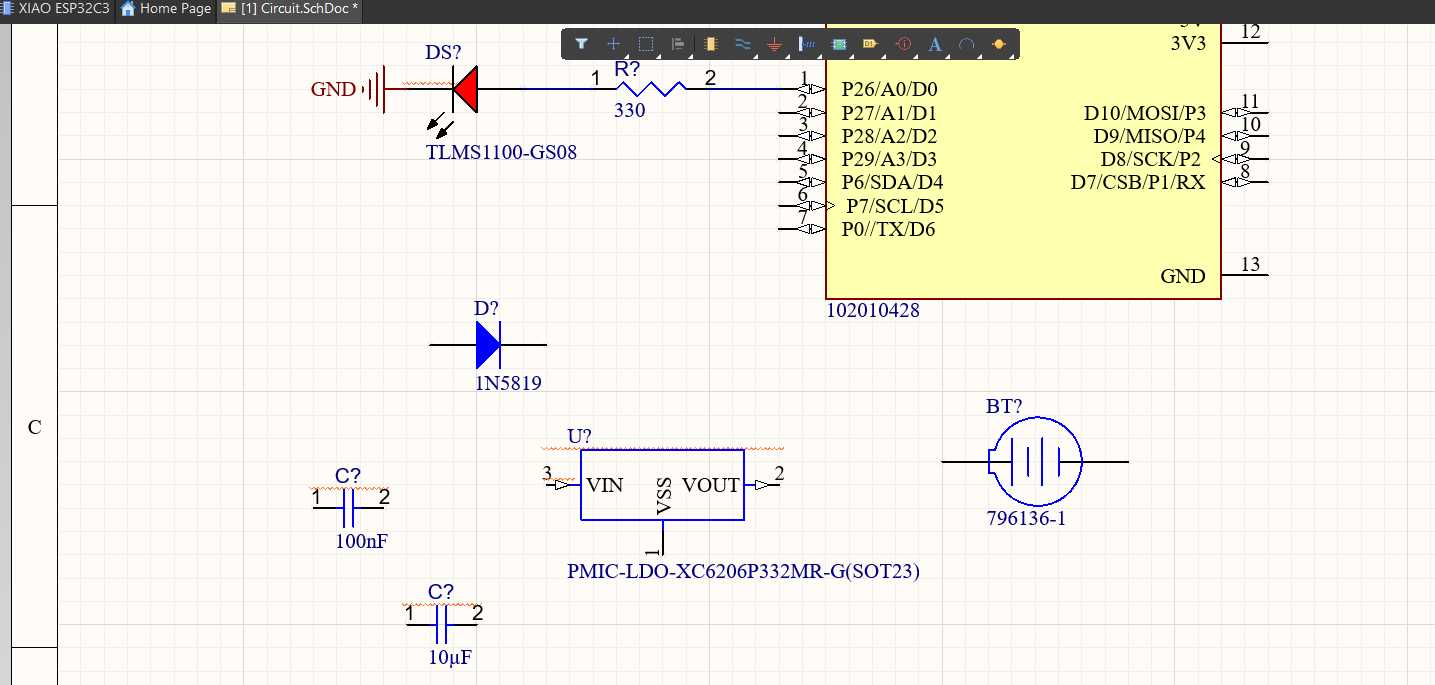
The microcontroller I used was a XIAO RP2040. To obtain the component, I used SnapMagic to search for it. I searched for the component with its footprint and downloaded the version compatible with Altium. It is important to log in before downloading components.
What is a footprint?
A footprint is the physical and graphical representation of pads and holes on a printed circuit board. Footprints are essential in CAD-based circuit design because they ensure precise assembly in production machines.
After downloading the component, I dragged it from the folder into the schematic and installed it. To place it, I searched for it in the Components panel, right-clicked, and selected Place.
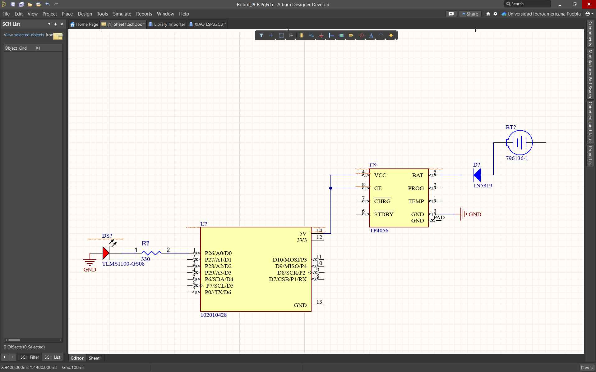
I began by placing an LED and a resistor. Then, I connected them to the microcontroller.
How to know which components to use?
For the calculation of resistances, Ohm's Law is used, which specifies: Resistance is equal to the source voltage minus the voltage drop divided by the current desired in the circuit. To determine the value needed for the capacitor, it must be known whether it is for signal filtering or smoothing, using the formula fc=1/2pi*R*C. .Whereas if it is for charging or discharging, the formula tau = R*C is used.
Next, I created a voltage regulator circuit using a diode, a battery, and two capacitors. I connected them to form the regulator circuit, which was then connected to the microcontroller.
Finally, I obtained a circuit where the battery voltage is regulated and an LED can be activated.
Design Rule Validation
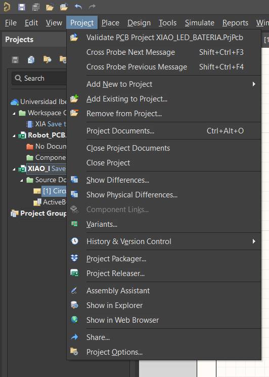
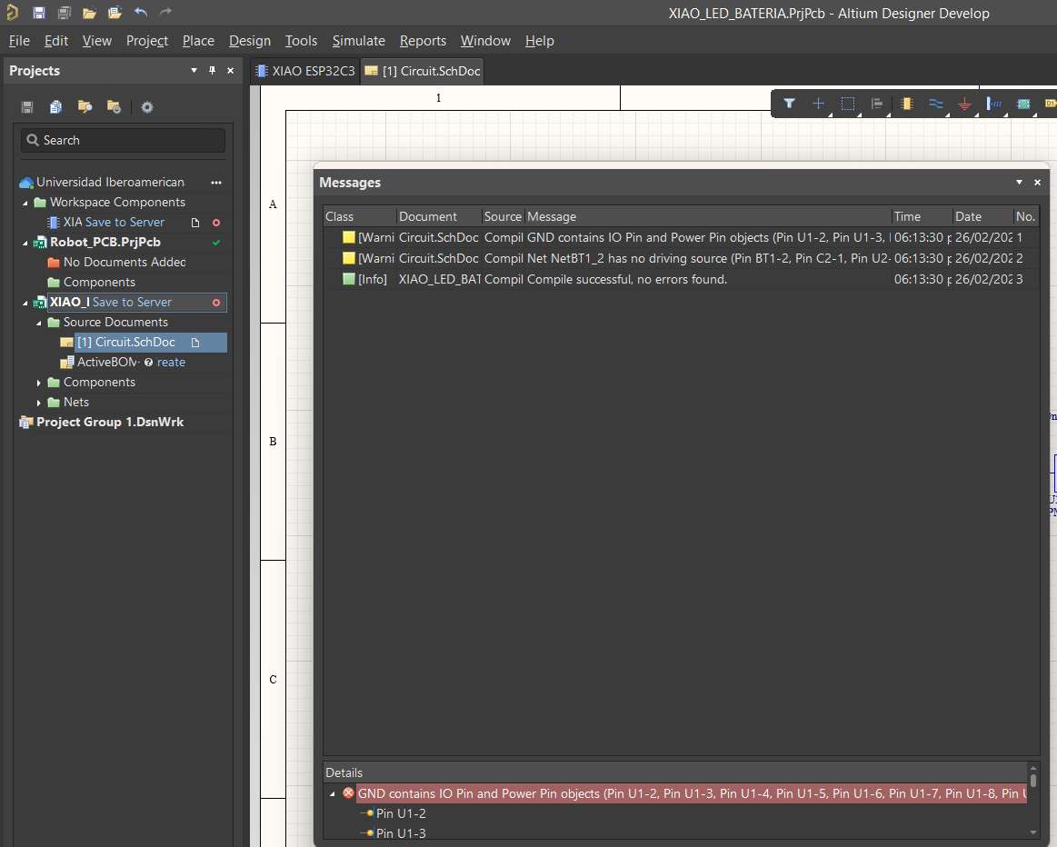
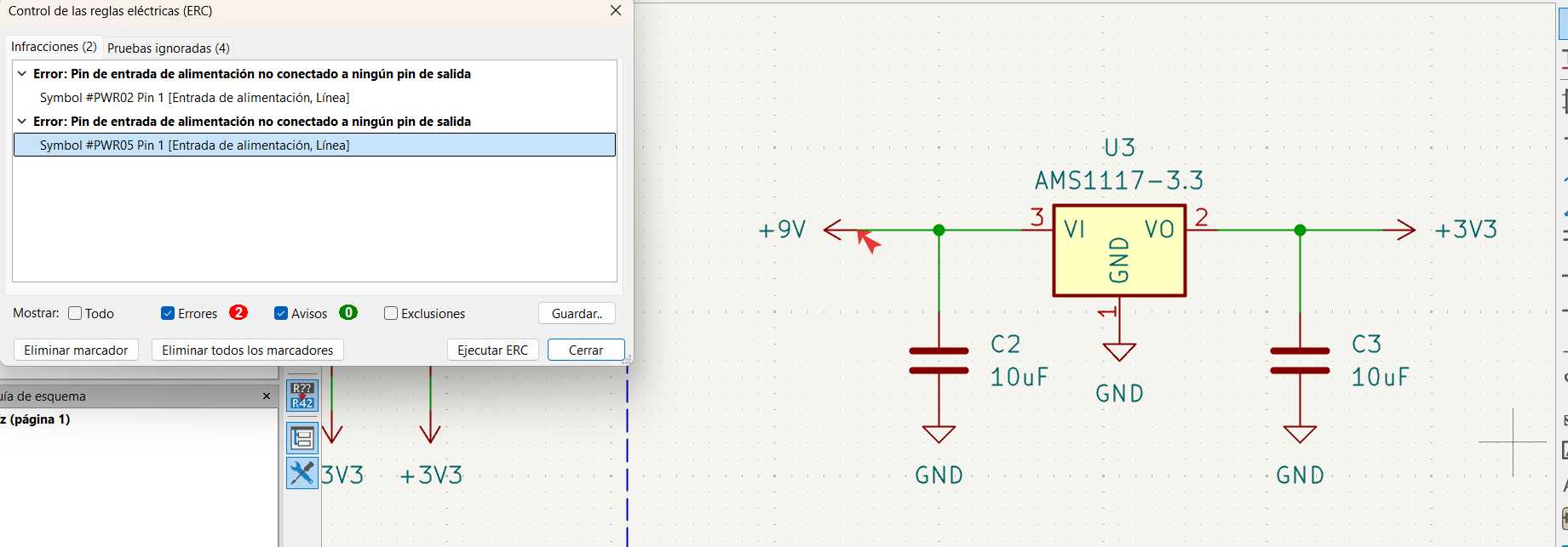
To verify that your design is correct, Altium provides a rule validation function. Select Project → Validate (Project Name), or right-click the project name and choose the same option.
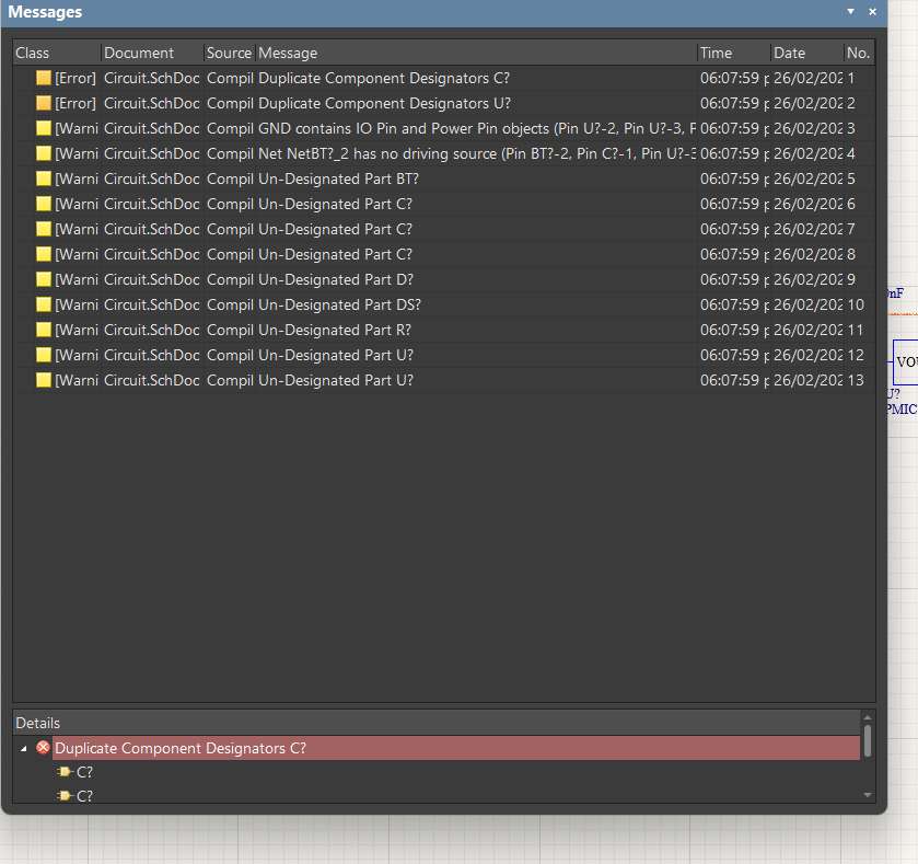
The Messages window will open, where you can see all the errors in your circuit. By selecting one of them, the program will take you directly to the schematic to visualize the issue.
Correct all errors until the project compiles successfully without any detected issues.
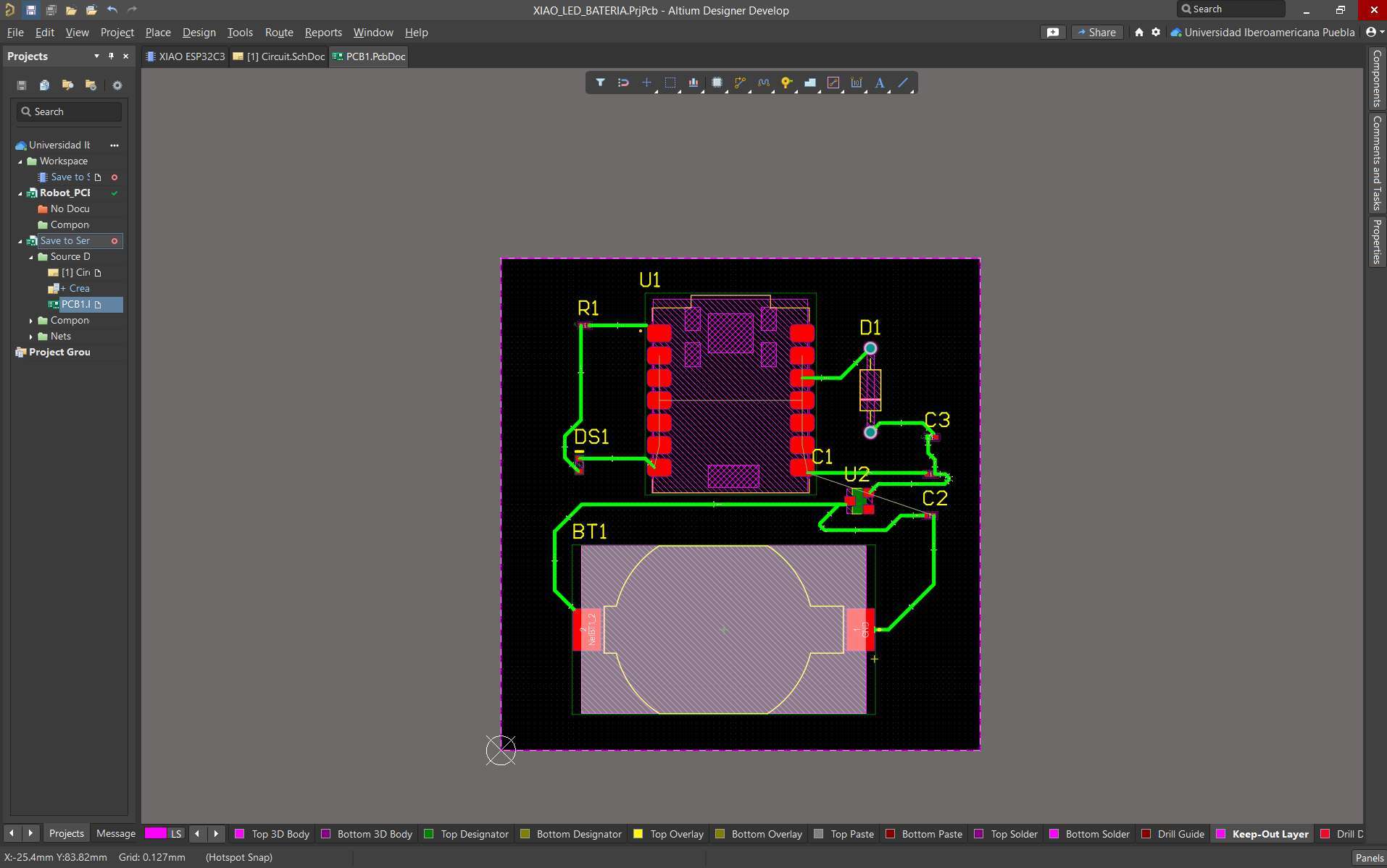
PCB Design
To convert the schematic into a PCB, first add a PCB document to the project and save it.
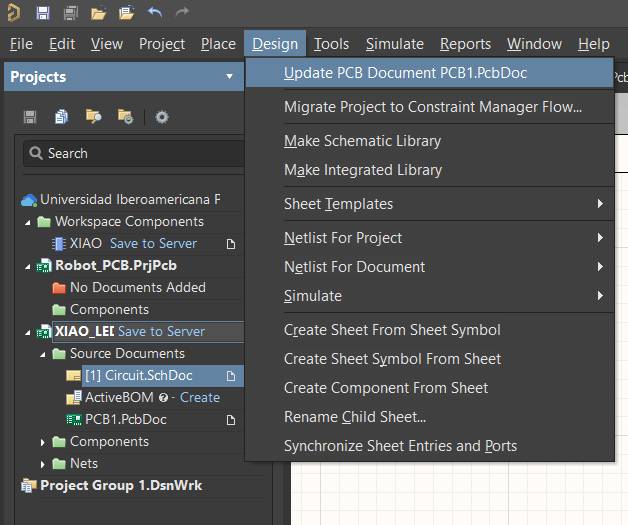
From the schematic, go to Design → Update PCB Document. A window will open where you must select Validate Changes, then Execute Changes. This will transfer the schematic to the PCB layout.
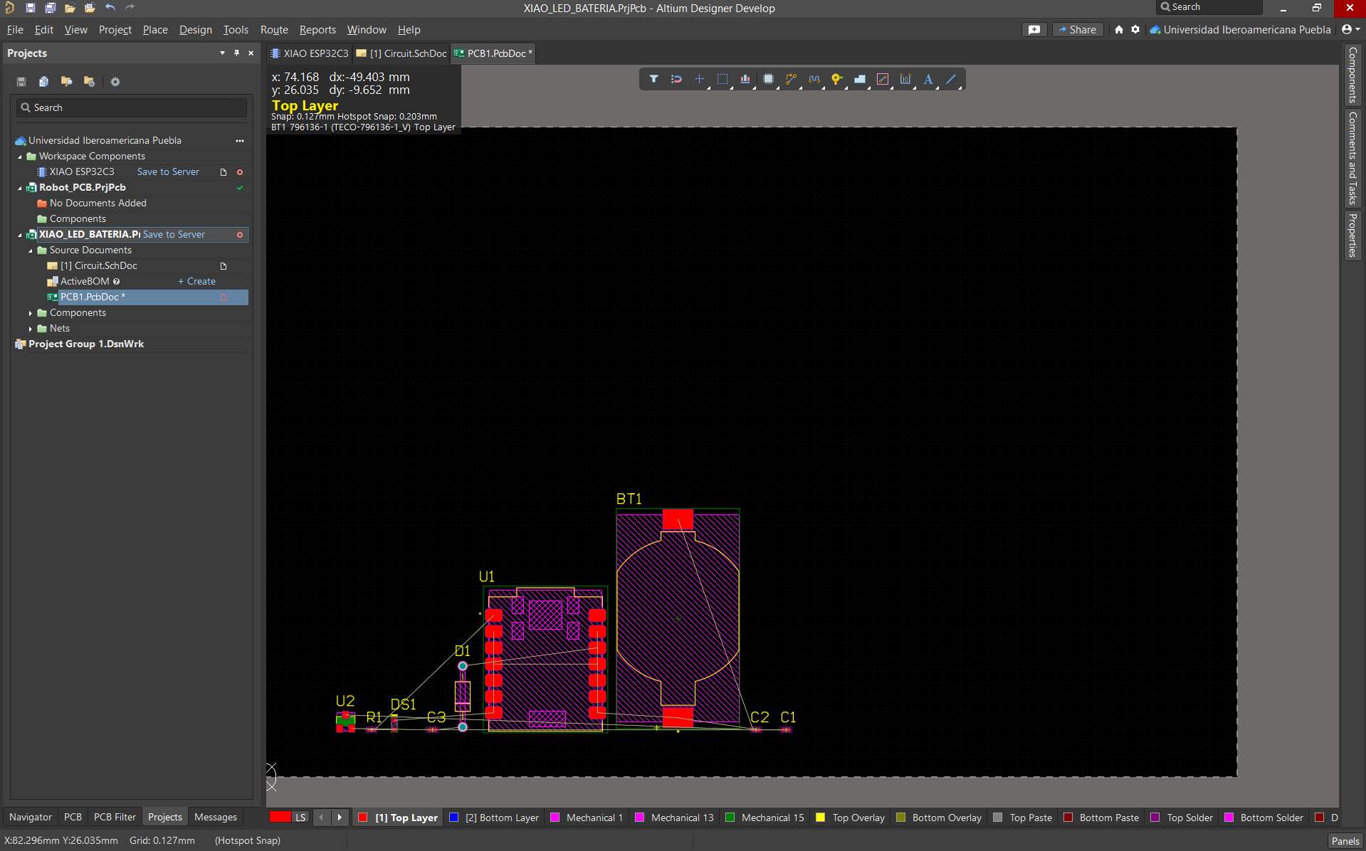
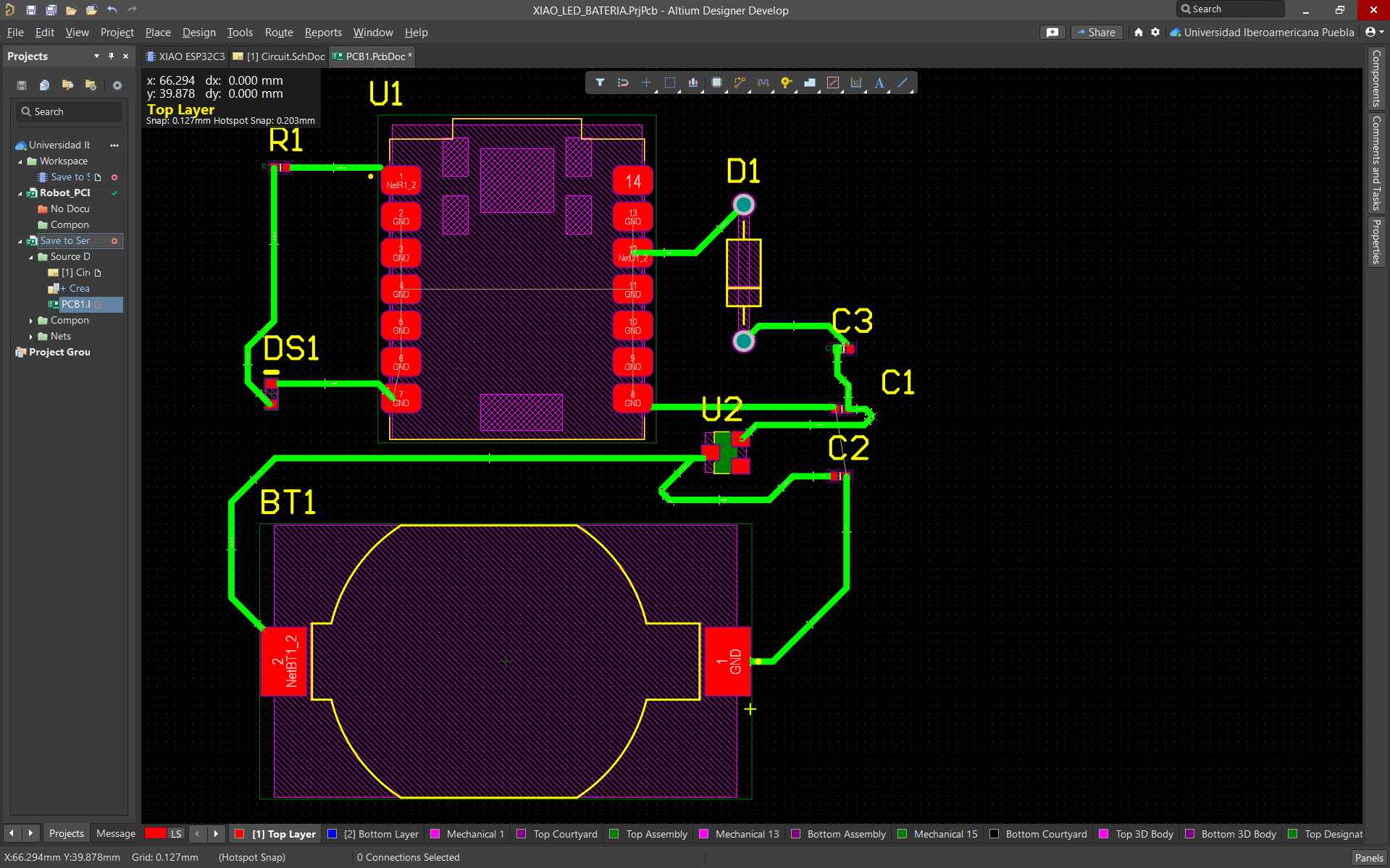
Arrange your components appropriately before starting the routing process.
To route connections, press Ctrl + W to activate the routing tool.
After completing the connections, use the line tool to mark the perimeter of the board. Then go to Design → Board Shape to define and trim the board to the specified area.
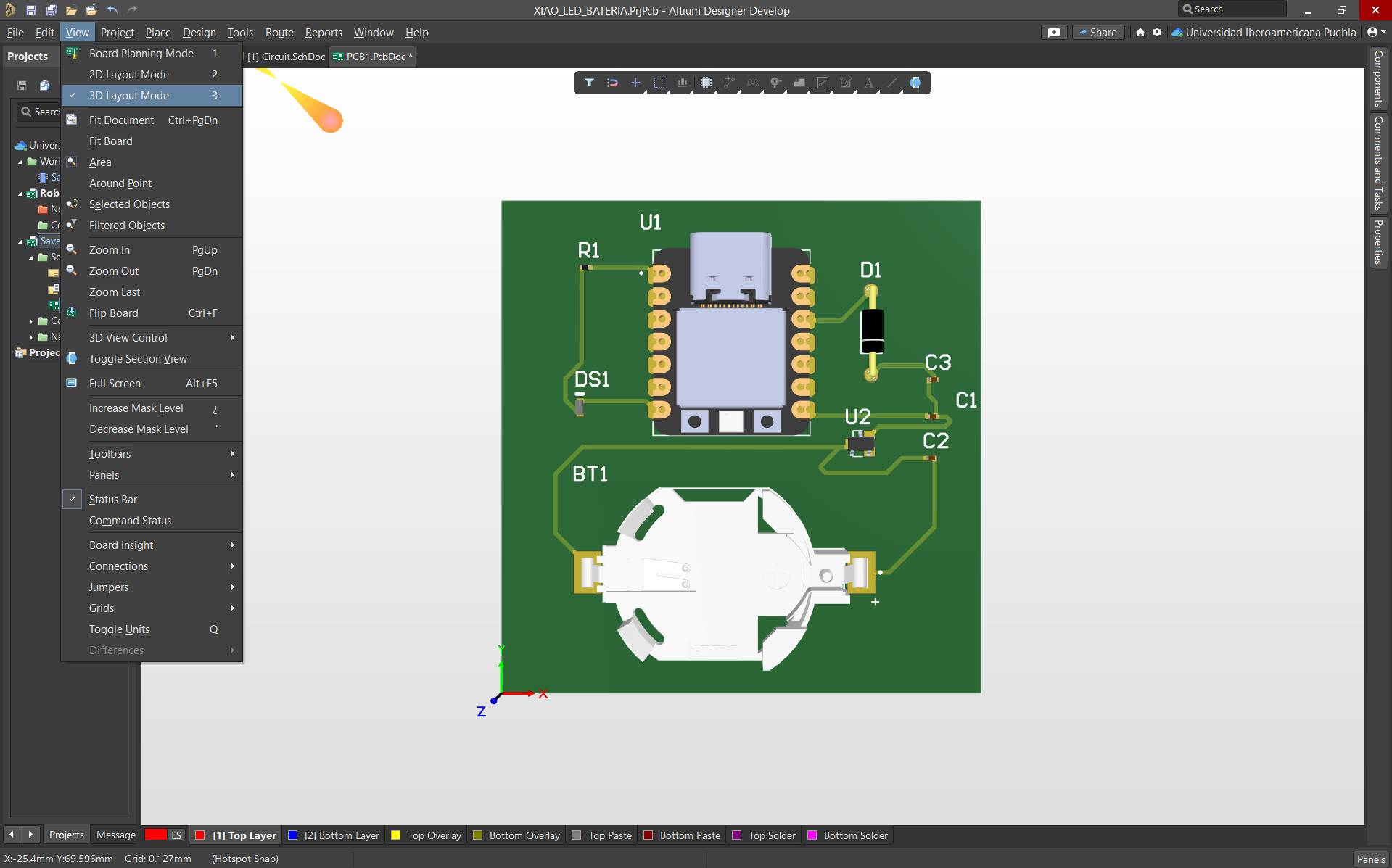
To activate the 3D viewer, press 3 or go to View → 3D Layout Mode.
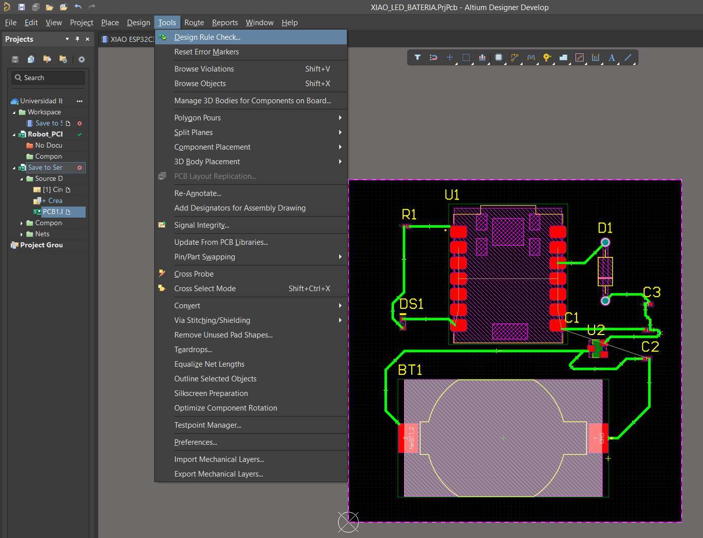
Design Rule Check
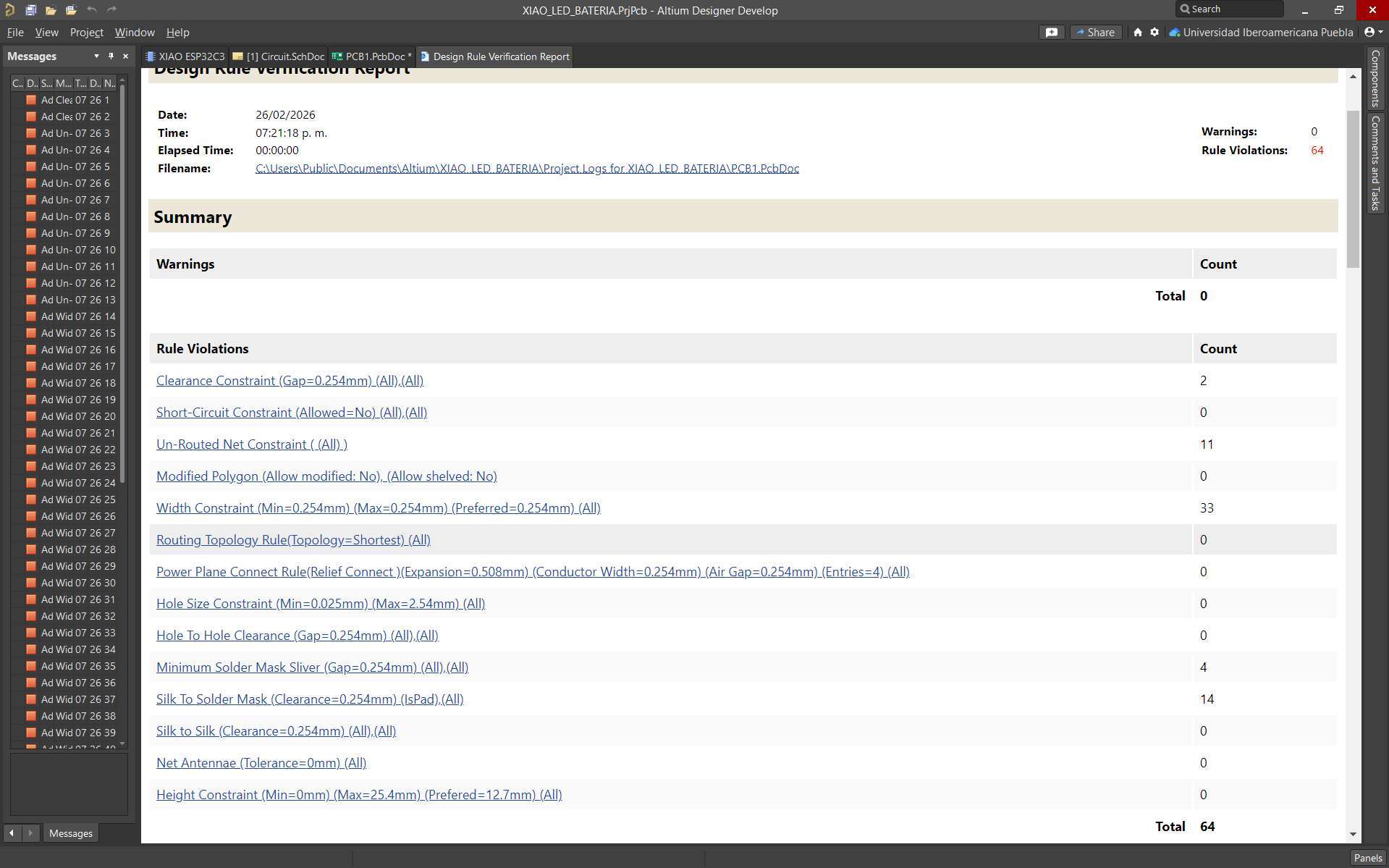
To verify that everything is correct, select Tools → Design Rule Check…. A window will appear. In the lower-left corner, select Run Design Rule Check…. The results will display the errors found.
To resolve them, select the rule that is not satisfied, and the program will take you directly to the PCB layout to better visualize the issue.
How to perform the simulation step by step?
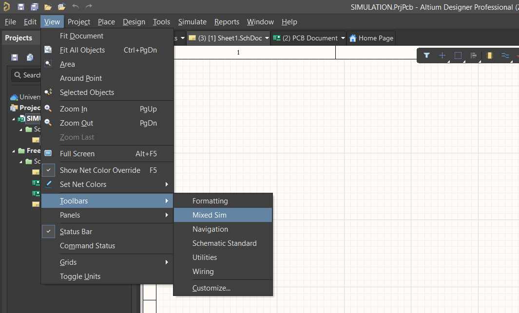
First, it must be ensured that the simulation extension is correctly installed.
After that, it was verified that the Mixed Sim tab was active. This can be activated by selecting View → Toolbars → Mixed Sim.
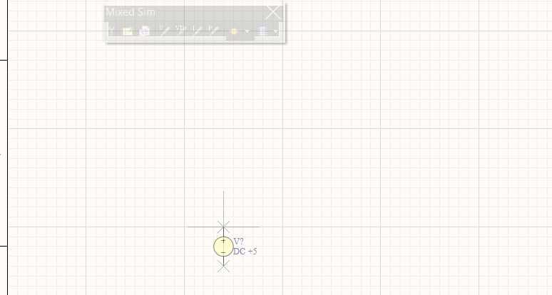
Subsequently, for this case, I created a new project where I could make a fairly simple simulation to demonstrate the steps that must be followed, where a new schematic was created.
A source was added for the simulation, where the resistors were connected. The wiring was carried out as previously explained.
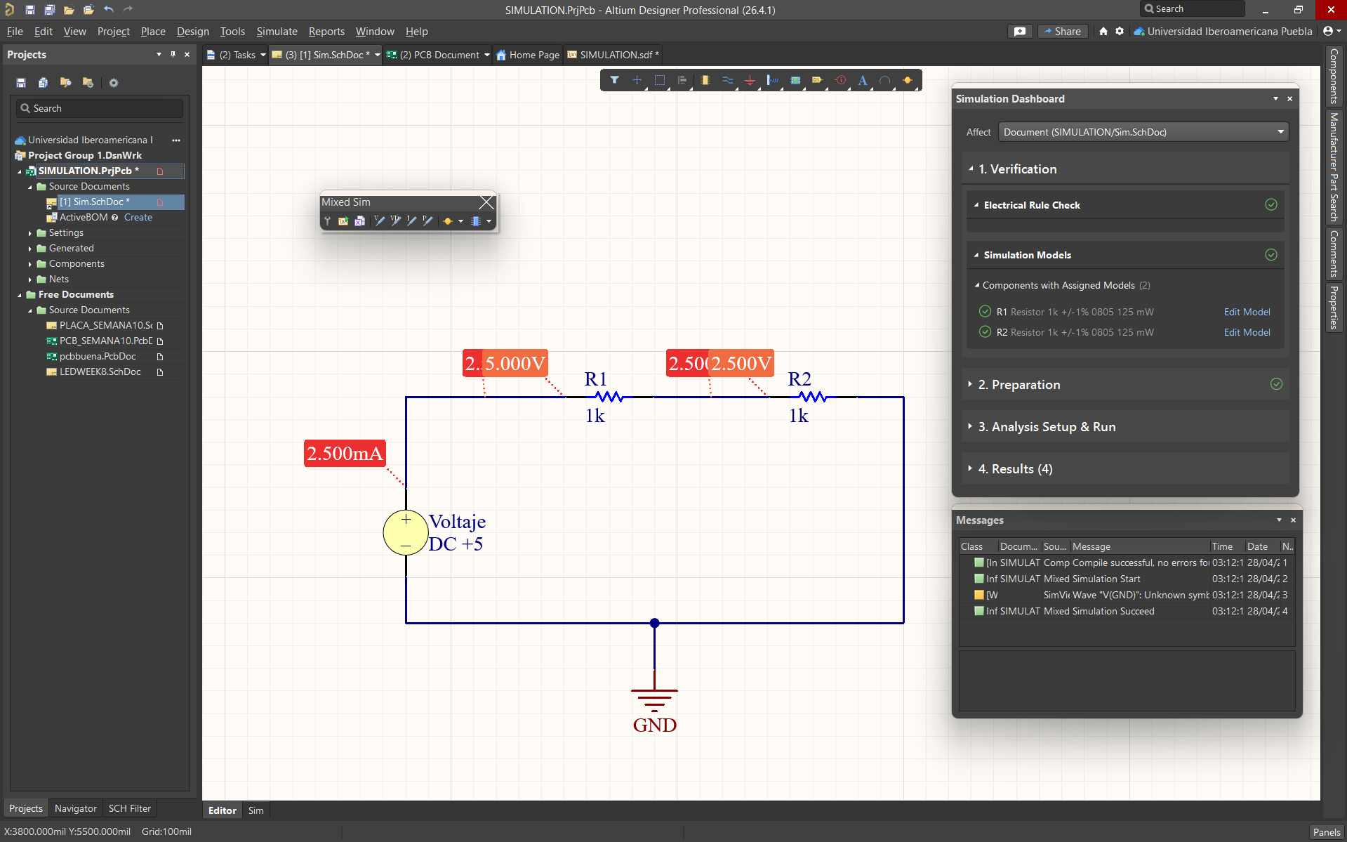
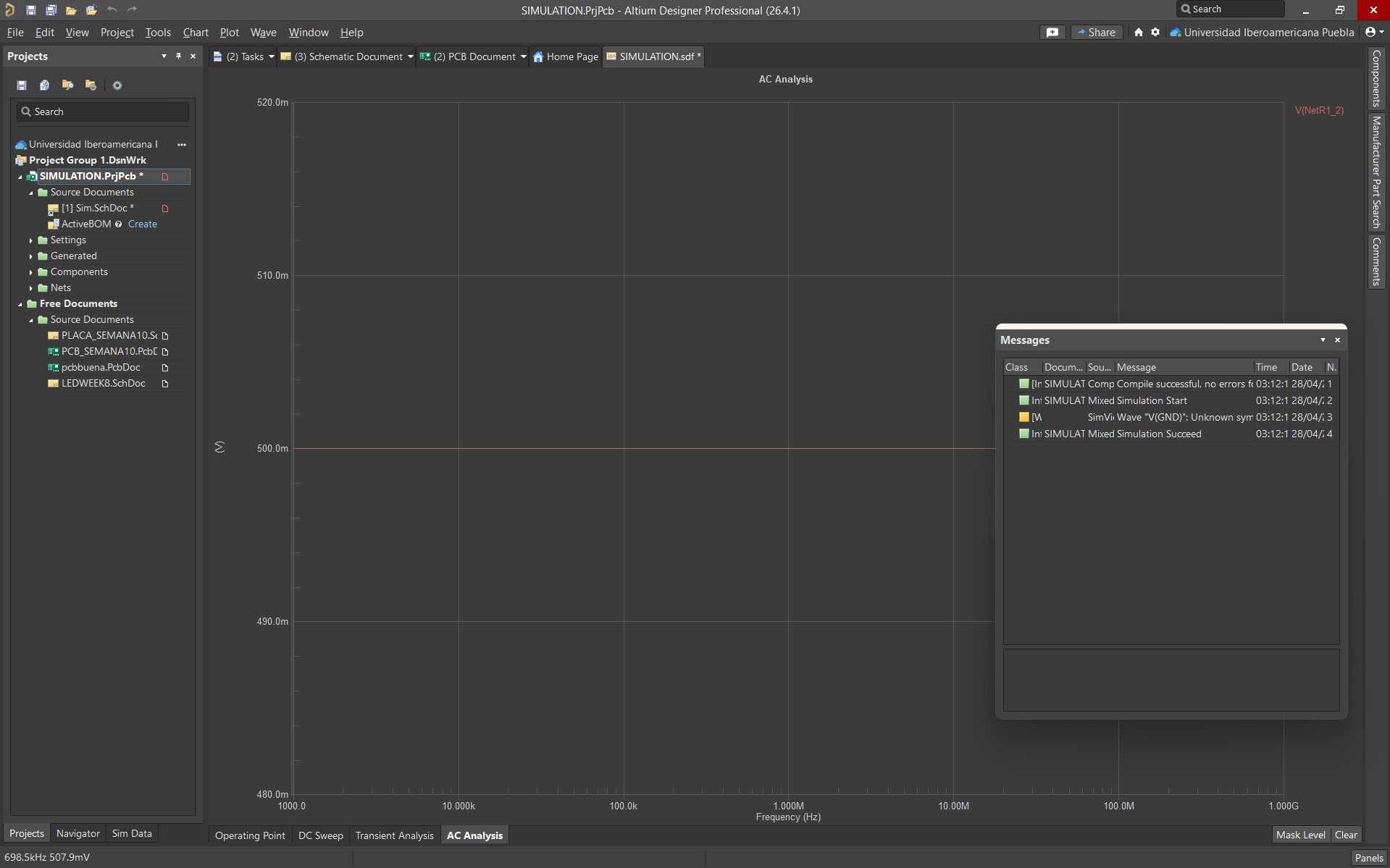
The icon to start the simulation is selected. This opens a window called Simulation Dashboard, where a series of steps to correctly perform the simulation are shown.
Finally, if everything is correct, you select start simulation again and this allows you to see the voltage values (in my case, what I selected) and a graph of it. Note: The graph shown is linear because the values are the same throughout the circuit.
Problems Encountered
KiCAD Schematic
Power input pin not connected to any output pin
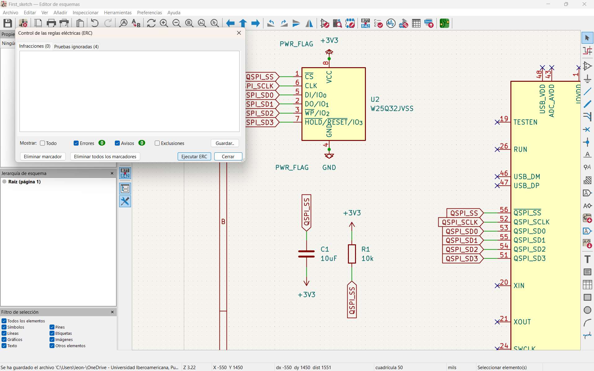
This occurs because the program does not recognize where the main voltage source is located. To solve this, press P and add a PWR_FLAG to the required inputs. This is a special symbol that tells the ERC where power originates.
Unconnected pin
It is important to know which pins you will use and ensure that all necessary pins are connected. If you want to indicate that a specific pin will not be used, press Q to add a no-connect flag.
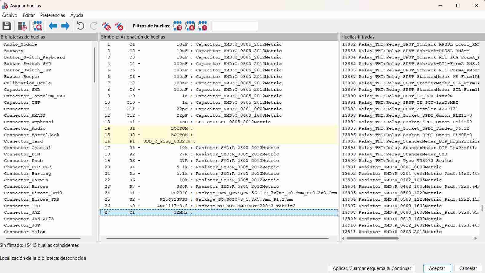
Footprint assignment
This is one of the most common errors. It can be resolved by selecting Tools → Assign Footprints. A window will open showing the components and their corresponding footprints. You can assign missing footprints there. Another method is to assign footprints component by component.
KiCAD PCB
Error due to unconnected components
I had a particular issue where I could not route a component because the software did not allow me to move in a certain direction. I solved it by reorganizing the upper traces, since their shape prevented the program from routing the remaining connections.
Board outline incorrectly defined
In my case, this occurred because I had not drawn the board outline. It was solved once I defined it properly.
Altium Schematic
Duplicate Component Designators
This is a common mistake when you are just starting. It usually occurs when components are copied and pasted without changing their names. The solution is to assign a unique name to each component. My solution was to open the Schematic Annotation Configuration panel, select Update Changes List, and allow the program to assign different numbers to the components. Then select Accept Changes (Create ECO), choose Validate Changes, and finally Execute Changes.
Messages tab not visible
This is easy to solve. In the lower right corner, select Panels and activate the Messages window from the list.
Altium PCB
Un-Routed Net Constraint (All)
This error appears when not all connections have been completed. Some components remain unconnected. The solution is to review which components show this error and complete their connections. Usually, a guiding line indicates which components should be connected.
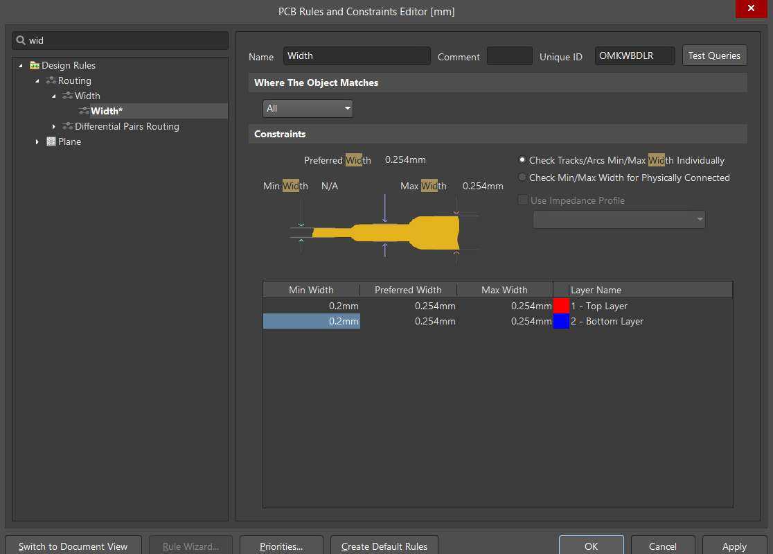
Width Constraint
This rule refers to the specified size of the traces. To modify it, go to Design → Rules… → PCB Rules and Constraints Editor → Width. There, you can change the values of your trace widths. It is important to define these values according to the manufacturing tools available.
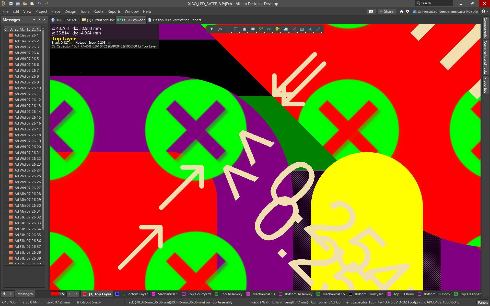
Minimum Solder Mask Sliver and Silk to Solder Mask
These warnings indicate that text is too close to or overlapping a copper pad. The Minimum Solder Mask Sliver warning appears when components have very closely spaced pins, resulting in a very thin solder mask between them. This means there could be a solder bridge if proper care is not taken during soldering. This rule can be disabled if necessary, as it is more related to PCB fabrication constraints.
Conclusions
This week allowed me to learn how to use two design programs to create electronic circuits. For me, completing this design was quite complex since I had no previous experience. However, it was extremely enriching to learn both programs. I felt more comfortable using KiCAD, and I preferred its interface because I consider it easier to understand when you are just beginning to design circuits. Nevertheless, Altium provides a large component library that is very useful during the design process. Both programs offer excellent tools for professionally designing electronic circuits.
If you want to access to my work from this week, please clickhere to download!
Finally, for the group assignment for this week, you can find the information here
 Finally, run the design rule check again to ensure everything is correct.
.png)
.png)