Week 09: Input devices
This week we were introduced to the concept of input devices in the context of microcontrollers, and, accordingly, this week's individual assignment required designing the PCB for an input device and interfacing it with the microcontroller PCB we manufactured the week prior in order to measure something. As part of this week's group assignment, the analog levels and digital signals of different input devices were tested. Click here to check on this week's group assignment page.
Work log
Completed tasks
- Designed a PCB for an input device.
- Interfaced the input PCB with the microcontroller PCB.
- Documented any problems encountered and how they were resolved.
1.What is an input device?
In the field of microcontrollers and embedded systems, input devices are hardware components that collect information regarding the environment, controller states, and user interactions. This data is subsequently converted into electrical signals that the system can utilize for further processing, data logging, and decision-making. For example, a microcontroller can receive input from:
| Input device | What it tells the microcontroller |
|---|---|
| Push button | Whether it is pressed or not |
| Potentiometer | The resistance value (voltage) |
| Temperature sensor | Heat at one location or element |
| Light sensor | Amount of illumination brightening an area |
| Ultrasonic sensor | Distance to an object |
| Encoder | Speed, position, or direction of rotation |
| Limit switch | Physical contact or absence of contact |
| Intertial Measurement Unit | Acceleration, rotation and position of an object |
Microcontrollers usually receive signals from input devices through input pins. These signals can be:
- Digital signals: Can either be HIGH or LOW, such as when a button is pressed or not pressed. Currently, a HIGH logic signal is typically around 3.3 volts, which is becoming the standard operating voltage for microcontrollers. However, 5-volt microcontrollers can still interpret both 3.3-volt and 5-volt signals.
- Analog signals: Analog signals can vary across a range of voltages, such as those produced by a potentiometer or light sensor. Similar to digital signals, the values of analog signals fall within specific voltage ranges, typically between 0 and 3.3 volts or 0 and 5 volts, depending on the microcontroller used.
Some input devices also communicate using protocols like I2C, SPI, UART, or CAN because they do more than just send a simple HIGH, LOW, or analog voltage. Many sensors contain their own internal electronics, which require a structured way to exchange data with a microcontroller.
2.Which input device did I choose to work with for this assignment?
As part of my robot modifications, I plan to implement several enhancements. I want to enable my transformable wheel legs to adopt intermediate poses, rather than only fully opening or closing. Currently, my setup uses linear actuators connected to each of the four individual wheel legs. Each actuator has two limit switches that detect when the wheel legs are fully opened or closed, which restricts the system to these two states.
My existing linear actuators consist of micrometal gear motors with a worm drive. I initially considered adding an encoder to each motor to track the number of spins needed to reach specific positions. However, my instructor advised against this approach, noting that a quadrature encoder would add unnecessary bulk to the overall design.
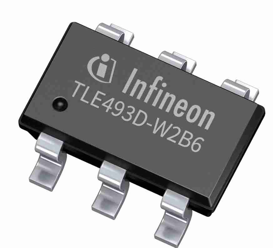
Instead, he recommended exploring the TLE493D sensor, a 3D magnetic sensor produced by Infineon Technologies. Incorporating this sensor into my design would necessitate adding a small magnet to the nut of my linear actuators. Before getting caught up in how to integrate it, I needed to ensure it would function correctly. I'd like to give a quick rundown of this sensor before talking about my progress this week.
The TLE493D sensor measures the three components of a magnetic field—Bx, By, and Bz—simultaneously. These measurements provide a complete vector representation of the magnetic field at the sensor's location, enabling a clear understanding of both the strength and direction of the field in three-dimensional space. It features a resolution of 12 bits per axis and offers a measurement range of up to ±160 mT, depending on the specific variant. This sensor is ideal for applications such as joystick position detection, knob rotation, linear position sensing, and current sensing through the magnetic field produced by a conductor.
The core of the sensor consists of Hall effect elements, which are thin semiconductor structures typically made of doped silicon. A bias current flows through these elements. When a magnetic field is present, the Lorentz force acts on the charge carriers, causing them to be deflected sideways. This deflection generates a small voltage that is perpendicular to both the current and the magnetic field. This voltage is referred to as the Hall voltage.
The TLE493D is regarded as a true 3D sensor because its Hall elements are arranged in three perpendicular planes. It features one horizontal element for measuring the Bz component and two vertical Hall elements that utilize a technique known as "spinning current" or "flux concentrators" for measuring the Bx and By components. However, measuring the lateral field components (Bx, By) with a flat silicon die presents challenges. To address this, Infineon employs integrated magnetic flux concentrators made of soft ferromagnetic material, which are deposited on top of the die to redirect the horizontal field lines downward into the vertical Hall element.
The TLE493D measures temperature in addition to magnetic fields. This measurement is primarily for magnetic compensation rather than environmental monitoring. Magnetic materials can change their field strength with temperature; for example, a permanent magnet weakens as it heats up. By monitoring the die temperature, the system can apply a correction factor to the Bx, By, and Bz readings, compensating for this drift and maintaining accurate magnetic measurements across a broad temperature range. Consequently, the temperature accuracy is specified as ±10°; it does not need to be highly precise, just sufficient to track trends. This function serves as an internal diagnostic tool integrated into the silicon, which is why it measures the chip's own die temperature instead of the ambient temperature.
The Hall voltages generated from measuring a magnetic field are in the microvolt range, making them barely perceptible to most commercial microcontrollers. Therefore, these signals are first processed through a low-noise instrumentation amplifier. Once amplified, the signal is then digitized using a 12-bit successive approximation analog-to-digital converter (ADC). This ADC is multiplexed across all three axes as well as the temperature sensor, which is why the four measurements occur sequentially in one conversion cycle rather than simultaneously.
The TLE493D is designed for low-pin-count embedded systems, which allows it to share data with a microcontroller via the I2C protocol. This sensor requires only four pins: VCC, GND, SDA, and SCL. The SDA and SCL pins are part of the I2C bus, enabling the connection of multiple sensors with different addresses for redundant sensing applications. While I2C is slower than SPI, this tradeoff is acceptable for a magnetic sensor that samples at a few hundred Hz.
After gaining a deeper understanding of the selected sensor, I designed a printed circuit board (PCB) for it and developed code to interface with it using a microcontroller.
If you wish to know more about this particular sensor, you can check its datasheet by clicking here.
3.PCB design
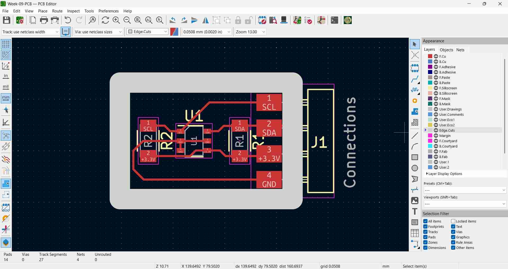
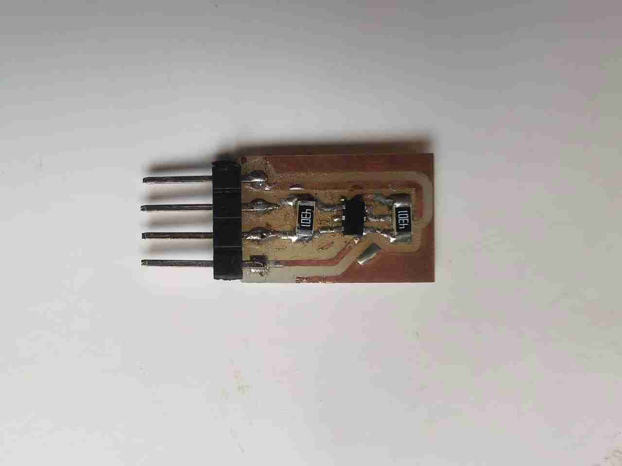
As with other electronics-related assignments, I designed this week's PCB using KiCAD. I based my design on the TLE493D footprint included in the fab library. I included two resistors for I2C, as specified in the datasheet. The datasheet recommends using 1.2 kilohm resistors; however, the lowest resistor value available at my fab lab when I designed and manufactured this PCB was 4.3 kilohms. I later determined that the change did not affect the performance or readings. Other elements present in the PCB schematic are four pin headers for connecting the VCC, GND, SDA, and SCL to the terminals.
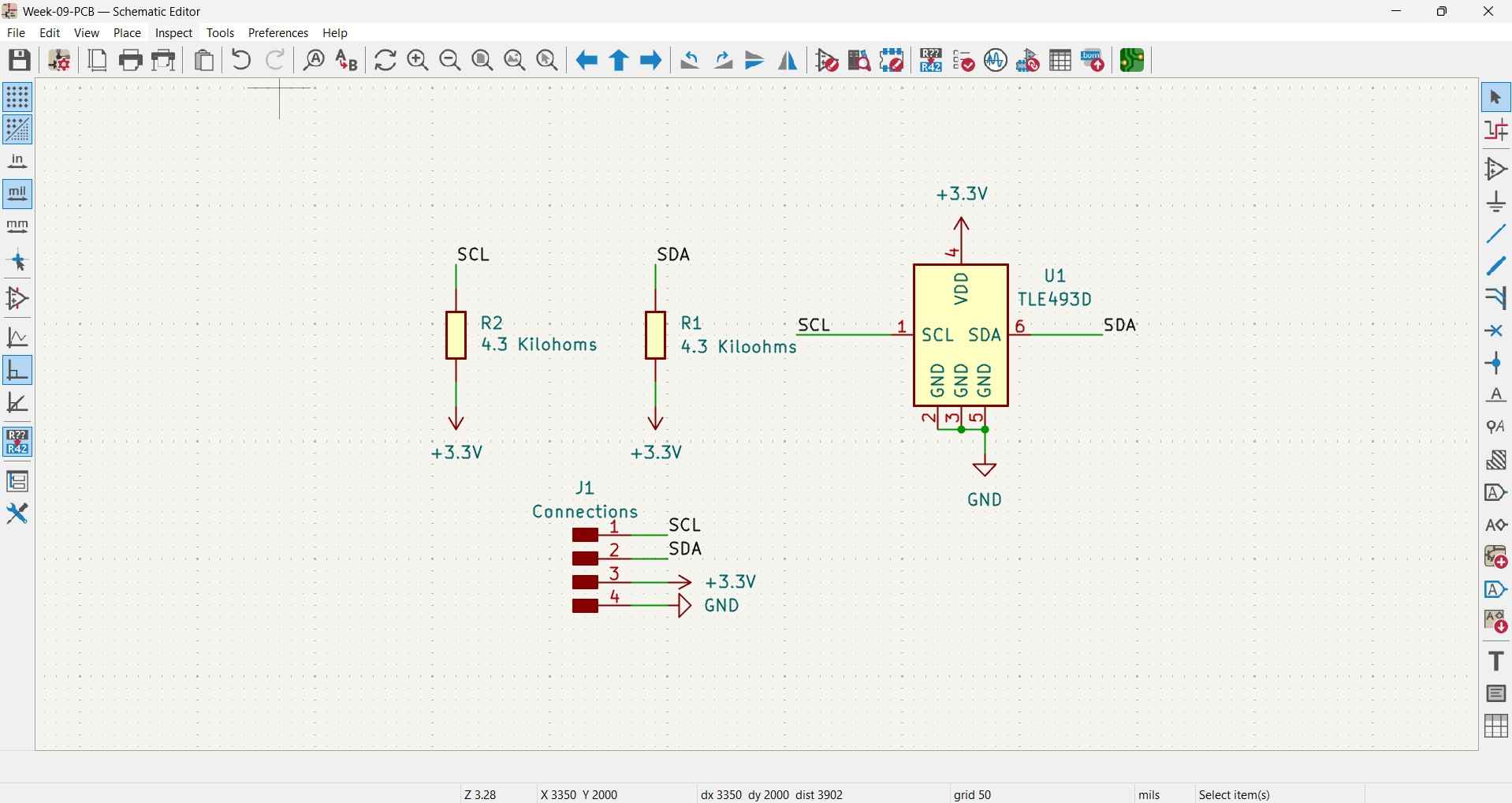
In an I2C bus, both SDA and SCL are open-drain lines, meaning that every device on the bus can only pull the line LOW, connecting it to GND through an internal transistor. No device actively drives the line HIGH; instead, the line goes HIGH passively through a pull-up resistor connected to VCC. Although communication is not the focus of this week's assignment, it is important to note that I2C communication allows for multiple devices, referred to as "targets," to receive commands and send data to a device known as the host. These terms were previously known as "slave" and "master," respectively. In an I2C bus, only target devices have an established address, which host devices use to identify each of their underlings and send commands.
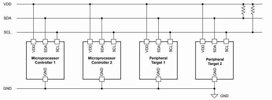
When there is no data exchange, all transistors are off, and the resistor pulls the line to 3.3V, indicating a logic HIGH. When a device wants to send a 0, it activates its internal transistor, pulling the line to GND, which represents a logic LOW. Once the device releases the transistor, the resistor restores the line to a HIGH state. If resistors were connected between two modules, this setup would not function properly because there would be no voltage source to pull the line HIGH. The resistor requires a reference voltage to pull toward it. Without VDD, when both devices let go of the line, it floats at an unknown voltage. This means that the bus would never get a clean logic HIGH, making communication completely unreliable. The pull-up resistor's role is specifically to source current from VDD into the bus line to return it to a known HIGH state after any device releases it. It does not filter noise or limit current between devices; rather, it actively defines the idle state of the bus.
The layout for the PCB was designed using the same rules and constraints mentioned in the Week 8 assignment , as the PCB would be manufactured using the Roland MonoFab machine.
The PCB's components were soldered using a soldering iron, again as described in the Week 8 assignment.
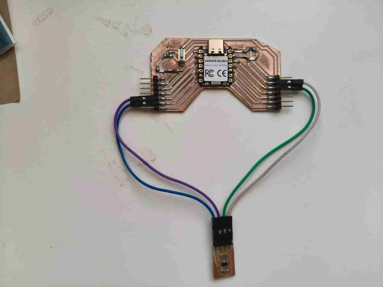
As I mentioned in the Week 4 assignment, I plan to use a Raspberry Pi Pico 2W board to control the motors of my robot. This means that both the encoders and TLE493D sensors will need to be connected to this board. Unlike the encoders, the I2C communication protocol will enable my design to consolidate sensor signals into just two traces. To test this sensor with the RP2350 chip found in the Pi Pico 2 and to avoid manufacturing a PCB for that specific board at this stage, I decided to use my Xiao RP2350 board, which I created for the Week 8 assignment.
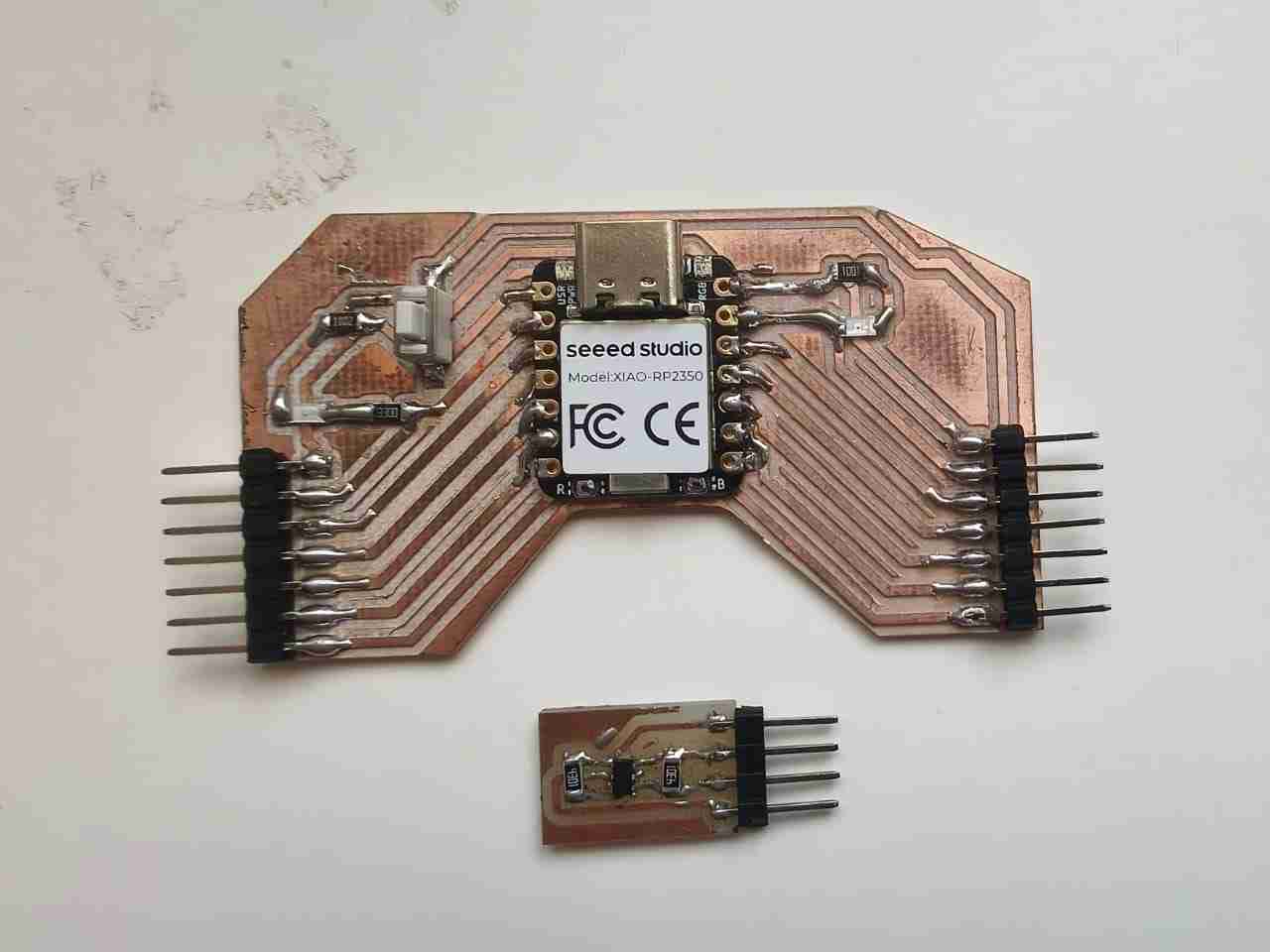
I want to highlight that the design of this PCB was not intentional; I did not realize that by connecting both PCBs with Dupont wires, the assembled circuit would adopt a heart-shaped appearance. I find that interesting.
4.Coding
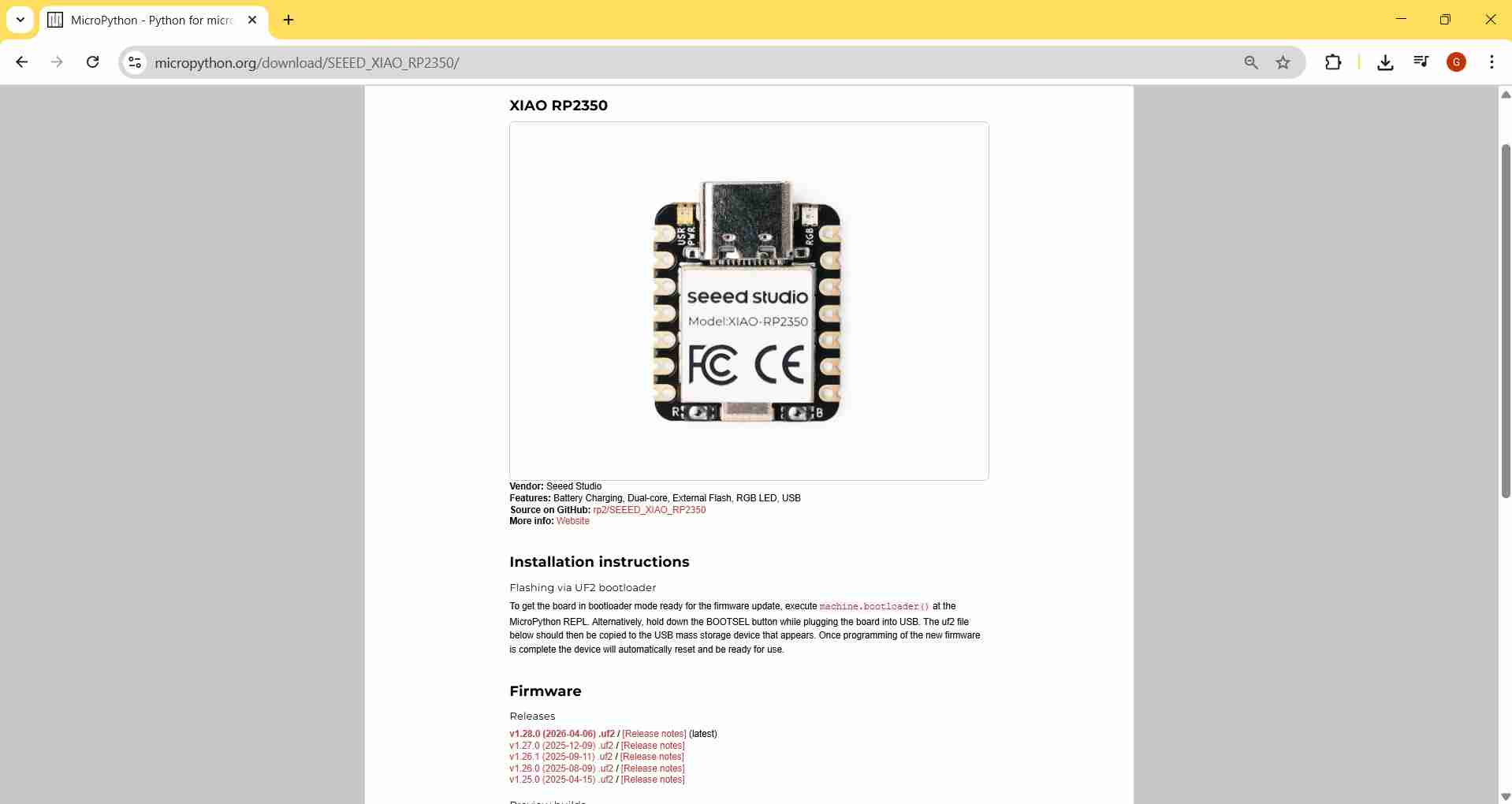
At first, my instructor advised me to write the code for my sensor using Thonny, as I wanted to gain more experience with the RP2350 running Python scripts. I did not object. Initially, I attempted to replicate the steps I had taken during my Week 4 assignment for my physical circuit, but unfortunately, it did not yield any results. I then visited the MicroPython website and realized that I needed to flash the Xiao RP2350 with its specific UF2 file, which I could download from the same website. I installed it using the same steps as during Week 4, but with this new file.
As I was becoming familiar with MicroPython, I utilized the Sonnet 4.6 model from Clause.ai for assistance. Although I am not particularly fond of vibe coding, I believe that using LLMs to learn how to code in various languages is a powerful educational tool.
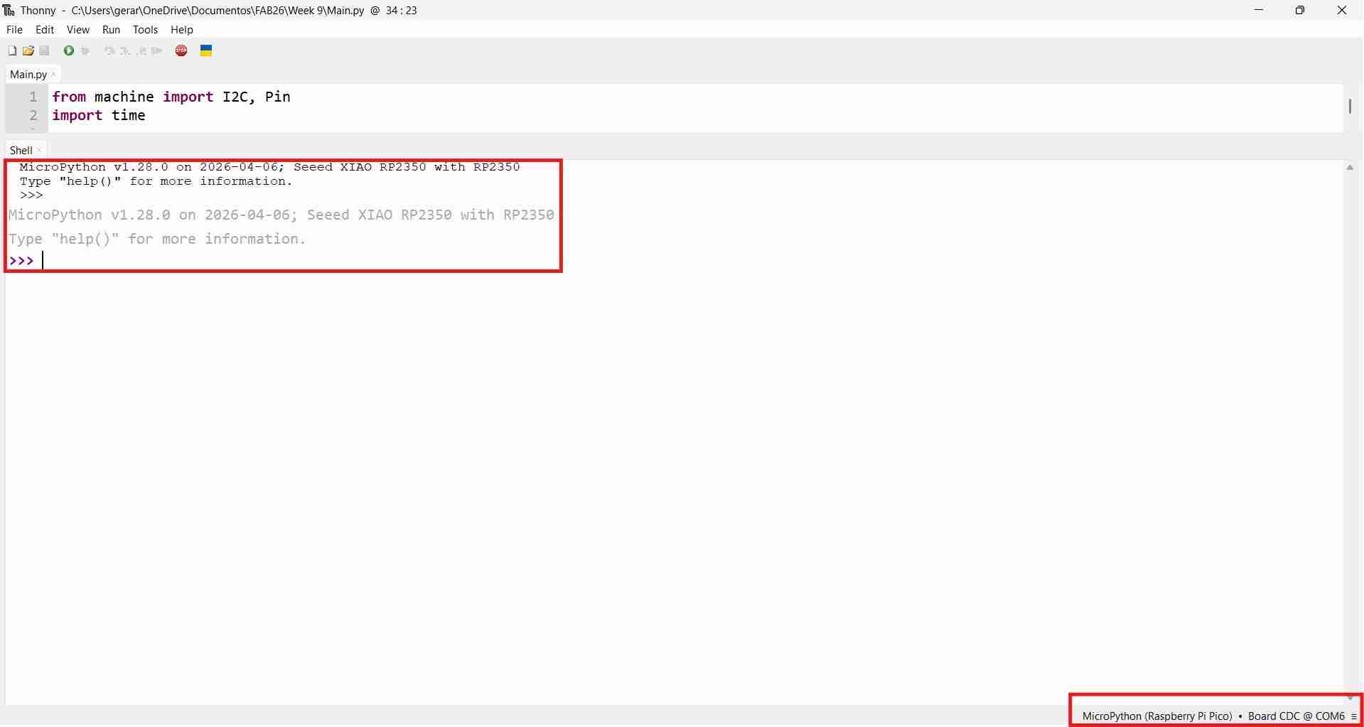
To ensure my PCB would function correctly, the first step was to verify that the I2C bus was operational. The Xiao RP2350, by default, exposes the Wire1/I2C (1) pins, which must be explicitly defined in the code. If I did not set SDA(6)/SCL(7) or define SDA as Pin(6) and SCL as Pin(7), the bus would fail to initialize properly. The following code confirmed that the actual I2C address for the sensor was 0×35.
          # MicroPython - First successful scan
          from machine import I2C, Pin
          i2c = I2C(1, sda=Pin(6), scl=Pin(7), freq=100000)
          print("Scan:", [hex(d) for d in i2c.scan()])
          # Output: ['0x35']
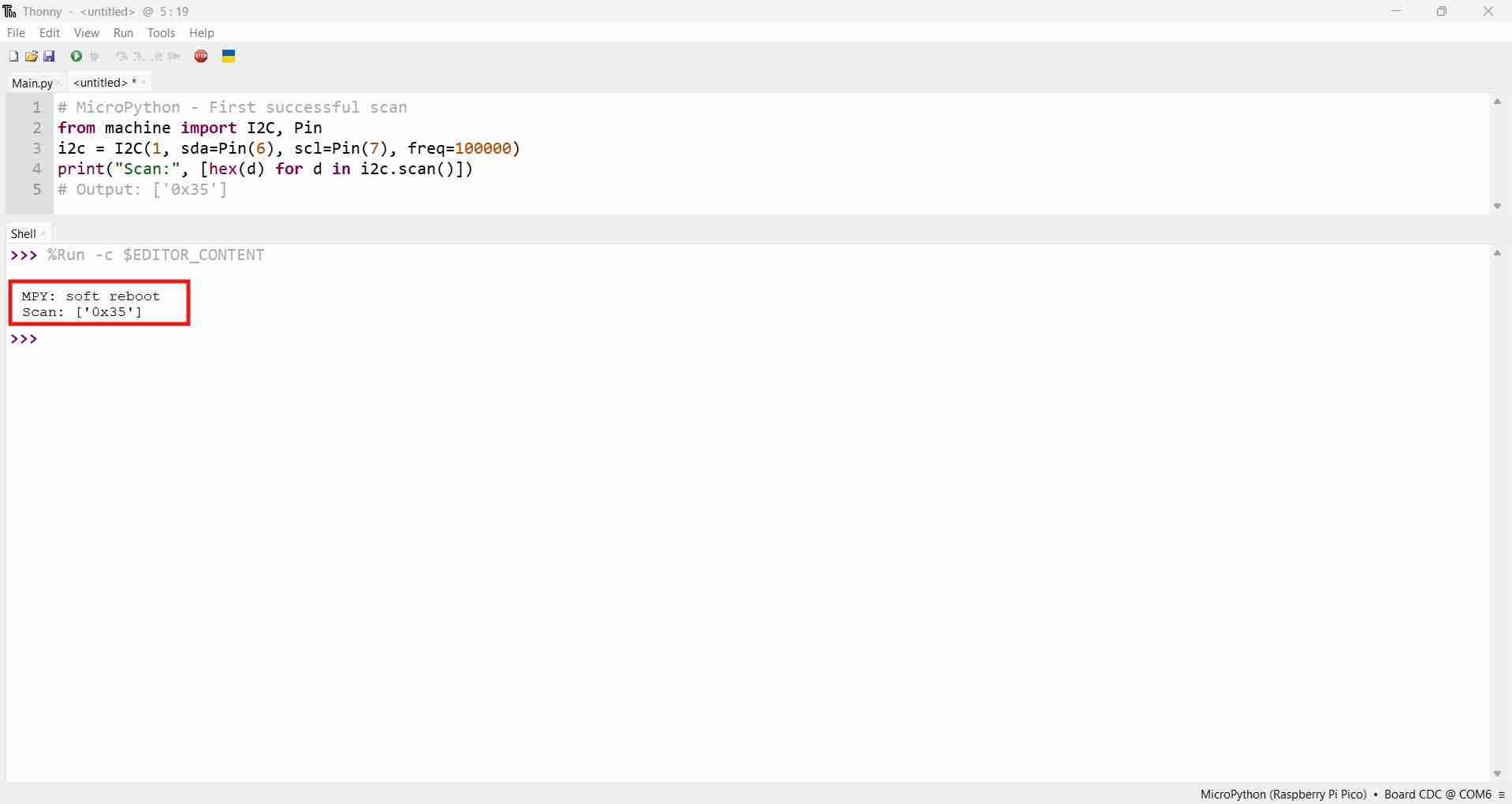
However, after comparing the 0x35 direction with those outlined in the datasheet, I realized that the direction displayed on the scanner didn't match any of the directions provided in the datasheet.
It took me some time to realize that the scanner was likely displaying a 7-bit address. According to the I2C standard, the first byte on the bus is structured as 7 address bits plus 1 R/W bit. Consequently, every I2C scanner reports 7-bit addresses, as the first byte is considered the actual device address by the protocol. However, some manufacturers express addresses in 8-bit format, which includes the full byte transmitted over the wire, along with the R/W bit.
| Bit | 7 | 6 | 5 | 4 | 3 | 2 | 1 | 0 |
|---|---|---|---|---|---|---|---|---|
| Field | A6 | A5 | A4 | A3 | A2 | A1 | A0 | R/W |
A 7-bit address can represent values from 0x00 to 0x7F (0 to 127 in decimal), while an 8-bit address can represent values from 0x00 to 0xFF (0 to 255). The address 0x35, which equals 53 in decimal, fits within the 7-bit range. Similarly, 0x6A, which equals 106 in decimal, also fits within 7 bits. Therefore, I could not verify the conclusion solely by the numbers, as both addresses could technically fit within the 7-bit limitation; I needed additional context.
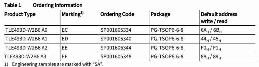
The datasheet explicitly shows pairs of 6AH/6BH, indicating that the pattern follows the 8-bit convention, where bit 0 serves as the R/W flag. A 7-bit address does not include a read/write variant; it represents only a single value. Typically, when datasheets provide two addresses for the same device—one for writing and one for reading—these are 8-bit values. The actual 7-bit address is obtained by shifting the write address right by 1. The following tables illustrate the conversion from 0×6A/0×6B to 0×35. Both conversions from the datasheet are represented in hexadecimal and binary. The blue cell in the shift row indicates the new bit 7, which is set to 0 during the right shift. The final bit of each original address (0 for writing, 1 for reading) is discarded, resulting in both addresses converging at 0x35 once the 7-bit address is expressed in binary.
| Step | 7 | 6 | 5 | 4 | 3 | 2 | 1 | 0 |
|---|---|---|---|---|---|---|---|---|
| 0x6A (write) | 0 | 1 | 1 | 0 | 1 | 0 | 1 | 0 |
| >> 1 (discard bit 0) | 0 | 0 | 1 | 1 | 0 | 1 | 0 | 1 |
| 0x35 (7-bit) | 0 | 0 | 1 | 1 | 0 | 1 | 0 | 1 |
| Step | 7 | 6 | 5 | 4 | 3 | 2 | 1 | 0 |
|---|---|---|---|---|---|---|---|---|
| 0x6B (read) | 0 | 1 | 1 | 0 | 1 | 0 | 1 | 1 |
| >> 1 (discard bit 0) | 0 | 0 | 1 | 1 | 0 | 1 | 0 | 1 |
| 0x35 (7-bit) | 0 | 0 | 1 | 1 | 0 | 1 | 0 | 1 |
After my initial attempt, I discovered that the 0×35 address corresponded to the 6AH and 6BH addresses from the A0 variant of the TLE493D-W2B6. This confirmed that the scanner was functioning properly and that I could effectively communicate with my sensor. I decided to convert the remaining addresses from the datasheet. If I was able to do it for one variant, why not continue with the others?
| Variant | Write (8-bit) | Read (8-bit) | Binary (write) | Shift right 1 | 7-bit (scanner) |
|---|---|---|---|---|---|
| A0 | 0x6A | 0x6B | 0b 0110 1010 | 0b 0011 0101 | 0x35 |
| A1 | 0x44 | 0x45 | 0b 0100 0100 | 0b 0010 0010 | 0x22 |
| A2 | 0xF0 | 0xF1 | 0b 1111 0000 | 0b 0111 1000 | 0x78 |
| A3 | 0x88 | 0x89 | 0b 1000 1000 | 0b 0100 0100 | 0x44 |
After confirming 0x35, the natural next step was to read the sensor's registers. This was the code:
          from machine import I2C, Pin
          import time

          i2c = I2C(1, sda=Pin(6), scl=Pin(7), freq=100000)
          addr = 0x35

          data = i2c.readfrom(addr, 10)
          for i, b in enumerate(data):
              print(f"Reg[0x0{i:X}] = 0x{b:02X}")
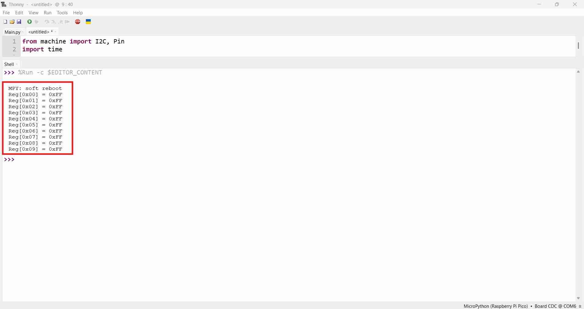
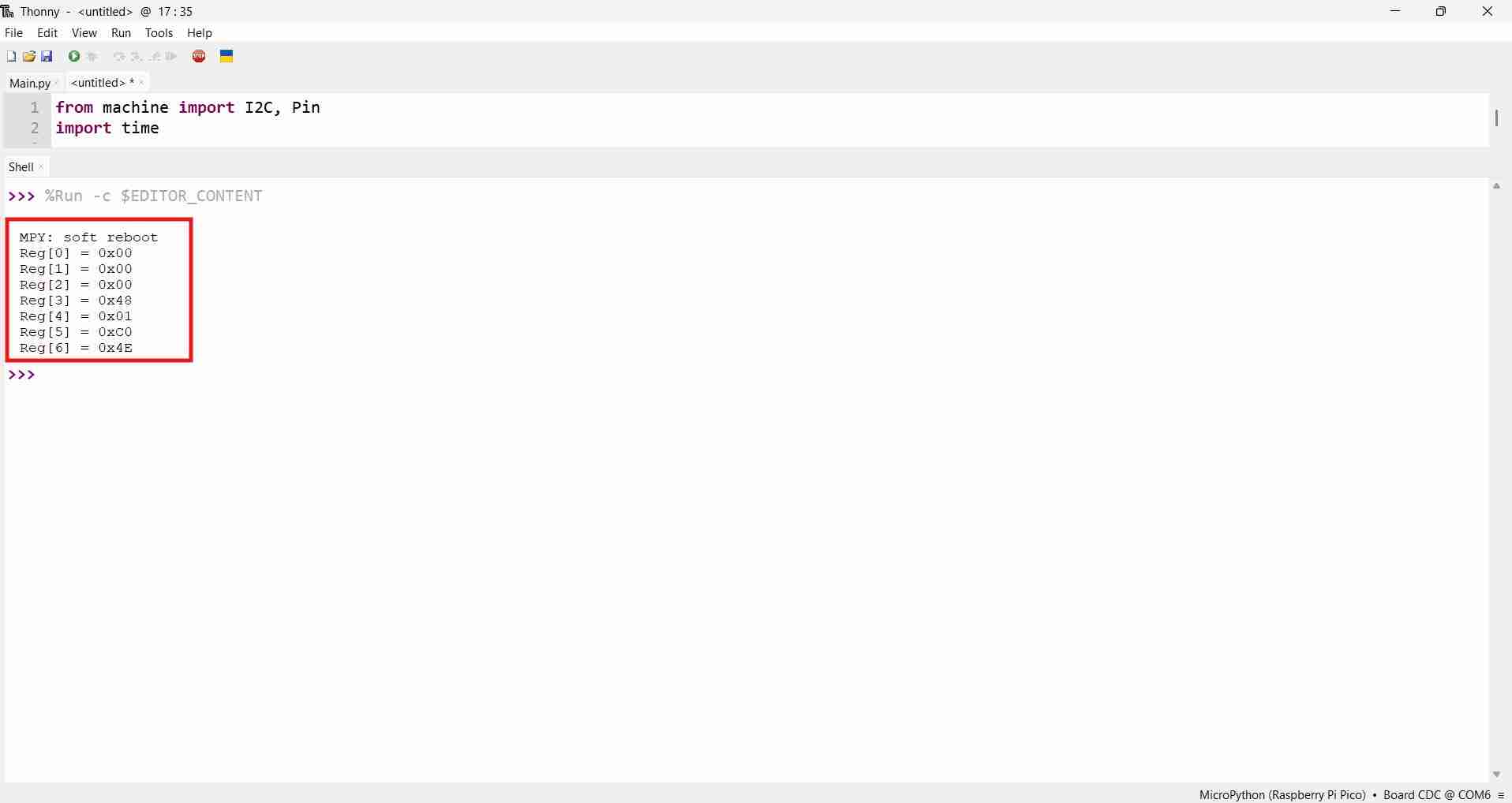
With this code, every register returned 0xFF. The sensor was physically present and acknowledged on the bus but did not deliver real data. Receiving 0xFF on every register is the I2C equivalent of a device holding SDA high permanently, meaning the sensor was receiving read requests but was unable to respond with actual data. At this point, I suspected hardware issues, including a damaged sensor, incorrect pull-up resistor values, and wrong voltage levels, and I spent a considerable amount of time ruling these out.
I connected the sensor PCB to a Raspberry Pi Pico 2W to determine whether the issue originated from the XIAO RP2350 or if it was something more serious. The Pico 2 produced the same results, indicating that the issue was not board-specific. The tests led me to conclude that the issue likely stemmed from the fundamental communication method I used with the sensor.
At this point, I decided to take a logical step: I delved deeper into the datasheet. This decision proved beneficial, as I discovered two crucial details. First, the minimum operating frequency for the sensor was 400 kHz, while I had been operating at 100 kHz. Consequently, I updated the frequency. Further investigation revealed the root issue: the TLE493D generates interrupt signals on the SCL line immediately upon power-on, even before any configuration is sent. These interrupts interfere with the I2C bus, causing every read to return 0xFF. The solution involved writing two configuration registers prior to attempting any reads.
          from machine import I2C, Pin
          import time

          # Corrected for XIAO RP2350
          i2c = I2C(1, sda=Pin(6), scl=Pin(7), freq=400000)
          time.sleep_ms(50)

          addr = 0x35

          i2c.writeto_mem(addr, 0x11, bytes([0x15]))
          time.sleep_ms(10)
          i2c.writeto_mem(addr, 0x10, bytes([0x20]))
          time.sleep_ms(50)

          data = i2c.readfrom(addr, 7)
          for i, b in enumerate(data):
              print(f"Reg[{i}] = 0x{b:02X}")
The initialization sequence was a game changer, as it allowed the microcontroller to access the register from the sensor and receive values other than 0xFF. This fact confirmed that the sensor requires explicit configuration before it delivers data. Without disabling the interrupt output, the sensor holds SCL low between conversions, which the I2C controller interprets as bus contention and fills the read buffer with 0xFF.
What each register does:
| Register | Address | Value | Effect |
|---|---|---|---|
| MOD1 | 0x11 | 0x15 | Switches to Master Controlled Mode and disables the INT pin that was blocking SCL |
| CONFIG | 0x10 | 0x20 | Tells the sensor to trigger an ADC conversion every time the controller initiates a read |
With the sensor now responding adequately, it was now time for reading actual data; the datasheet register map indicated how the 7 bytes were structured. The magnetic values are 12-bit integers split across multiple registers. The code for reading magnetic and temperature values is the following:
        from machine import I2C, Pin
        import time

        i2c = I2C(1, sda=Pin(6), scl=Pin(7), freq=400000)
        time.sleep_ms(50)

        addr = 0x35

        # Mandatory initialization
        i2c.writeto_mem(addr, 0x11, bytes([0x15]))
        time.sleep_ms(10)
        i2c.writeto_mem(addr, 0x10, bytes([0x20]))
        time.sleep_ms(50)

        while True:
            data = i2c.readfrom(addr, 7)

            # Reconstruct 12-bit values from split registers
            # Bx: upper 8 bits in data[0], lower 4 bits in upper nibble of data[4]
            Bx = (data[0] << 4) | (data[4] >> 4)
            # By: upper 8 bits in data[1], lower 4 bits in lower nibble of data[4]
            By = (data[1] << 4) | (data[4] & 0x0F)
            # Bz: upper 8 bits in data[2], lower 4 bits in lower nibble of data[5]
            Bz = (data[2] << 4) | (data[5] & 0x0F)

            # Two's complement sign extension: if bit 11 is set, value is negative
            if Bx & 0x800: Bx -= 4096
            if By & 0x800: By -= 4096
            if Bz & 0x800: Bz -= 4096

            # Temperature: 10-bit value scaled to 12-bit range
            temp_raw = (data[3] << 2) | (data[6] >> 6)
            temp_c = (temp_raw * 4 - 1180) * 0.24 + 25

            print(f"Bx={Bx:5d}  By={By:5d}  Bz={Bz:5d}  Temp={temp_c:.1f}C")
            time.sleep_ms(200)
What each decoding step does:
| Value | Registers used | Operation | Reason |
|---|---|---|---|
| Bx | data[0], data[4] | (data[0] << 4) | (data[4] >> 4) | MSB in full byte, LSB in upper nibble of shared register |
| By | data[1], data[4] | (data[1] << 4) | (data[4] & 0x0F) | MSB in full byte, LSB in lower nibble of shared register |
| Bz | data[2], data[5] | (data[2] << 4) | (data[5] & 0x0F) | MSB in full byte, LSB in lower nibble of status register |
| Temperature | data[3], data[6] | (data[3] << 2) | (data[6] >> 6) | 10-bit value split across two registers |
| Sign extension | — | if value & 0x800: value -= 4096 | Converts unsigned 12-bit to signed (two's complement) |
| Temp formula | — | (raw × 4 − 1180) × 0.24 + 25 | Scales raw ADC value to degrees Celsius per datasheet coefficients |
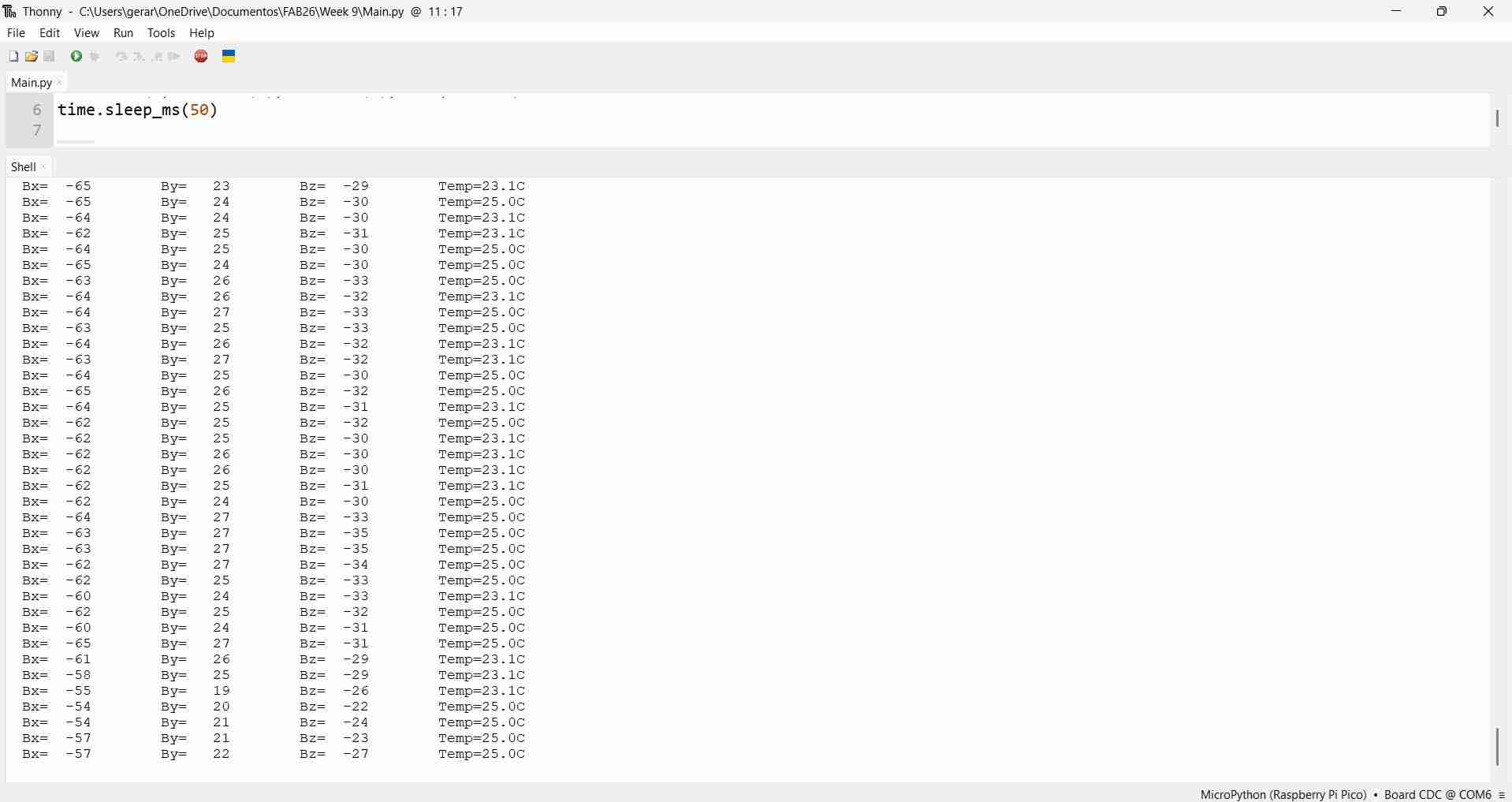
After the microcontroller could process data from the sensor, I decided to test if the readings could respond to changes in the magnetic field. So I decied to test two stacks of magnets.
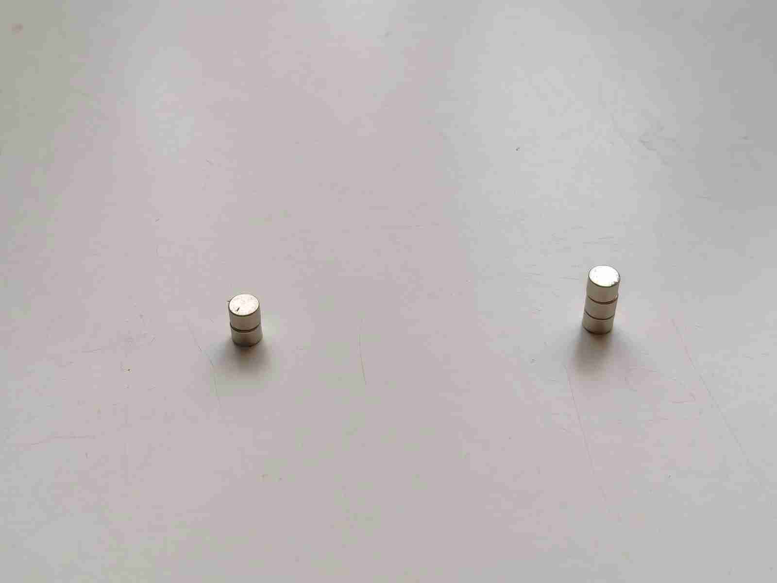
I first placed one stack of magnets near the sensor and recorded the readings. The following image shows the results from the two-magnet stack. The fact that the values changed in the presence of a magnet showed that the sensor was truly functional.
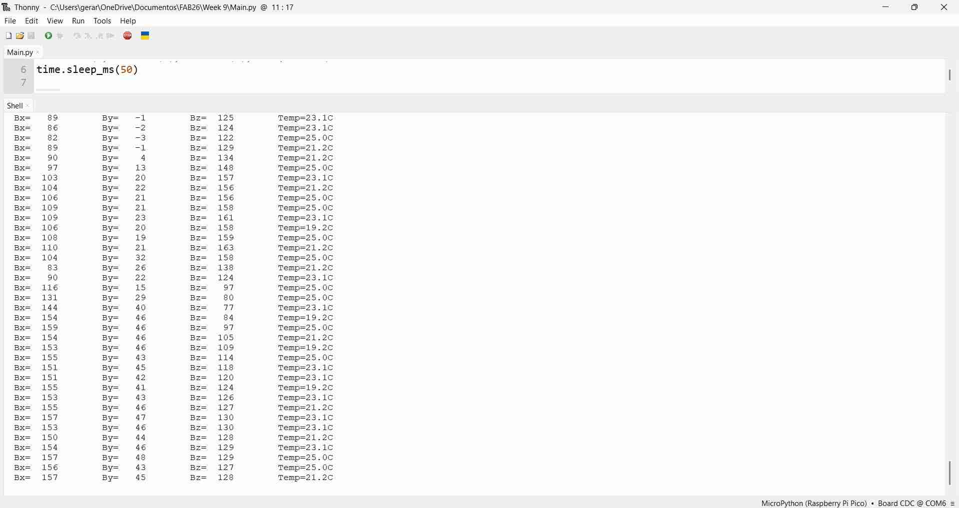
The following image shows the results from the three-magnet stack. By simply looking at the magnetic values, which were significantly greater than those from the two-magnet stack, it was clear that the sensor could detect the presence of multiple magnets.
The next video shows the sensor in action with multiple magnets:
5. Files
Here are the downloadable files for this week:
KiCad schematic and codeReflection
I must admit that by the end of this assignment, I have developed a strong trust in LLMs. However, reading through the datasheet gave me valuable insight into how the sensor works. I also refreshed my knowledge of I2C. I anticipate that I will be using it again in the near future.