Week 08: Electronics Production
This week, we were introduced to electronics production, which involves converting circuit schematics into physical electronic components. Our main focus was on manufacturing a microcontroller printed circuit board that will serve as the foundation for our electronics-related assignments. For this week's group assignment, we characterized the design rules for the PCB fabrication processes available at FabLab Ibero Puebla, along with their machine settings. Additionally, we documented the workflow for sending a PCB to a boardhouse. Click here to check on this week's group assignment page.
Work log
Completed tasks
- Described the process of tool-path generation, milling, and soldering.
- Described the workflow used and identified potential issues.
- Manufactured a microcontroller PCB.
1.What is PCB milling?
Printed circuit board milling is a technique used to produce printed boards by mechanically cutting away copper from a copper-clad board using a CNC machine. Instead of chemically dissolving unwanted copper, a small rotating bit removes copper around the traces, pads, and holes. This method is also referred to as isolation milling, as the tool creates insulating gaps around the conductive copper paths.
Before desktop CNC milling machines became ubiquitous, the go-to method for PCB manufacturing among hobbyists and labs involved chemical etching. In this process, a circuit pattern is transferred onto a copper-clad board, and then chemicals such as ferric chloride or another etchant are used to dissolve the exposed copper. This method is proven and reliable; however, it involves chemical handling, staining, waste disposal, ventilation concerns, and cleanup. PCB milling avoids most of these issues because the copper is removed mechanically rather than chemically. The main concerns with using PCB milling include avoiding fiberglass phenolic boards, as inhaling their dust can pose cancer risks. Additionally, the milling machine should be enclosed and vacuumed whenever a PCB is manufactured.
PCB milling has gained popularity due to the increased affordability of small CNC machines, the simplification of controller electronics, advancements in open CNC software, and the greater accessibility of PCB design software through student licenses and open-source options. These developments have effectively bridged the gap between industrial production and hobbyist use. As a result, PCB milling has become a practical solution for schools, makerspaces, labs, and engineers, allowing them to produce PCBs in-house rather than waiting for a board house or handling etching chemicals. The primary advantage of PCB milling is its speed for prototyping. For a simple single-sided or double-sided PCB, the processes of designing, milling, drilling, and soldering can all be completed within the same day. This efficiency is particularly beneficial for quickly testing circuits that may require several revisions.
PCB milling has not fully replaced chemical etching or industrial PCB fabrication. Chemical and photolithographic methods are favored for mass production because they can produce finer features, such as plated through-holes, solder masks, silkscreens, and multilayer boards, while ensuring consistent results in high volumes. Milling is better suited for rapid prototyping, simple boards, educational purposes, and low-volume production, rather than for the dense PCBs commonly found in modern smartphones. Moreover, milled boards may exhibit different behaviors in RF and high-frequency applications due to variations in geometry and the amount of remaining copper when compared to etched boards
The basic workflow for PCB milling is:
- Design the PCB using EDA software
- Export the design to a suitable format for milling, typically Gerber format
- Transform manufacturing files into CNC toolpaths
- Secure a copper-clad board onto the machine bed
- Drill holes if necessary
- Mill the board to remove unwanted copper and create traces
- Cut out the outline of the board
2.Manufacturing files creation for a single-sided PCB with no drill holes
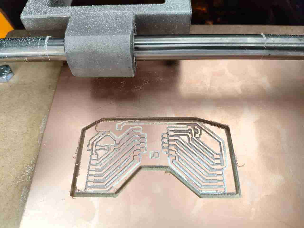
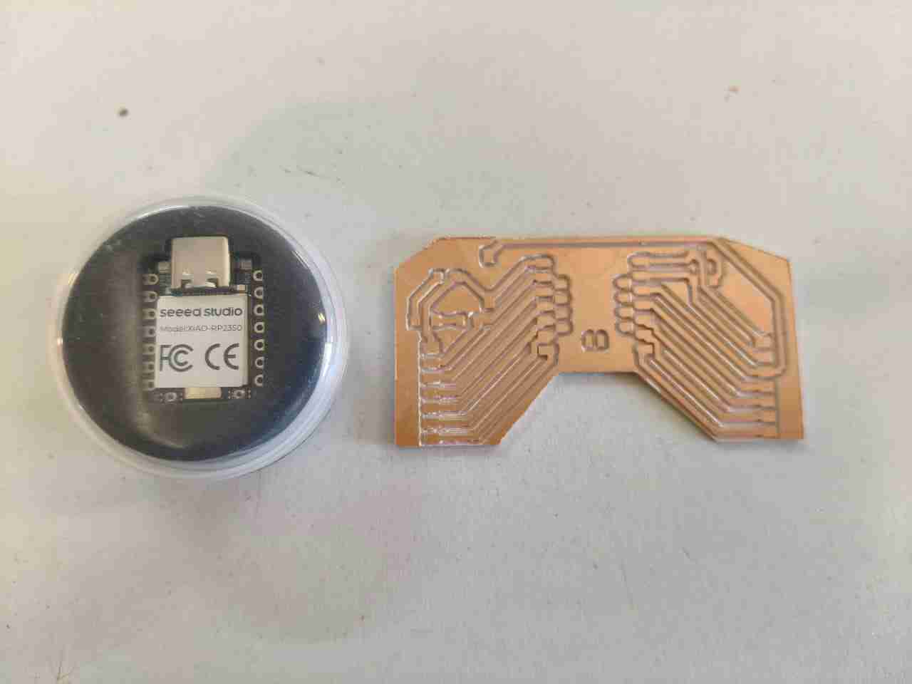
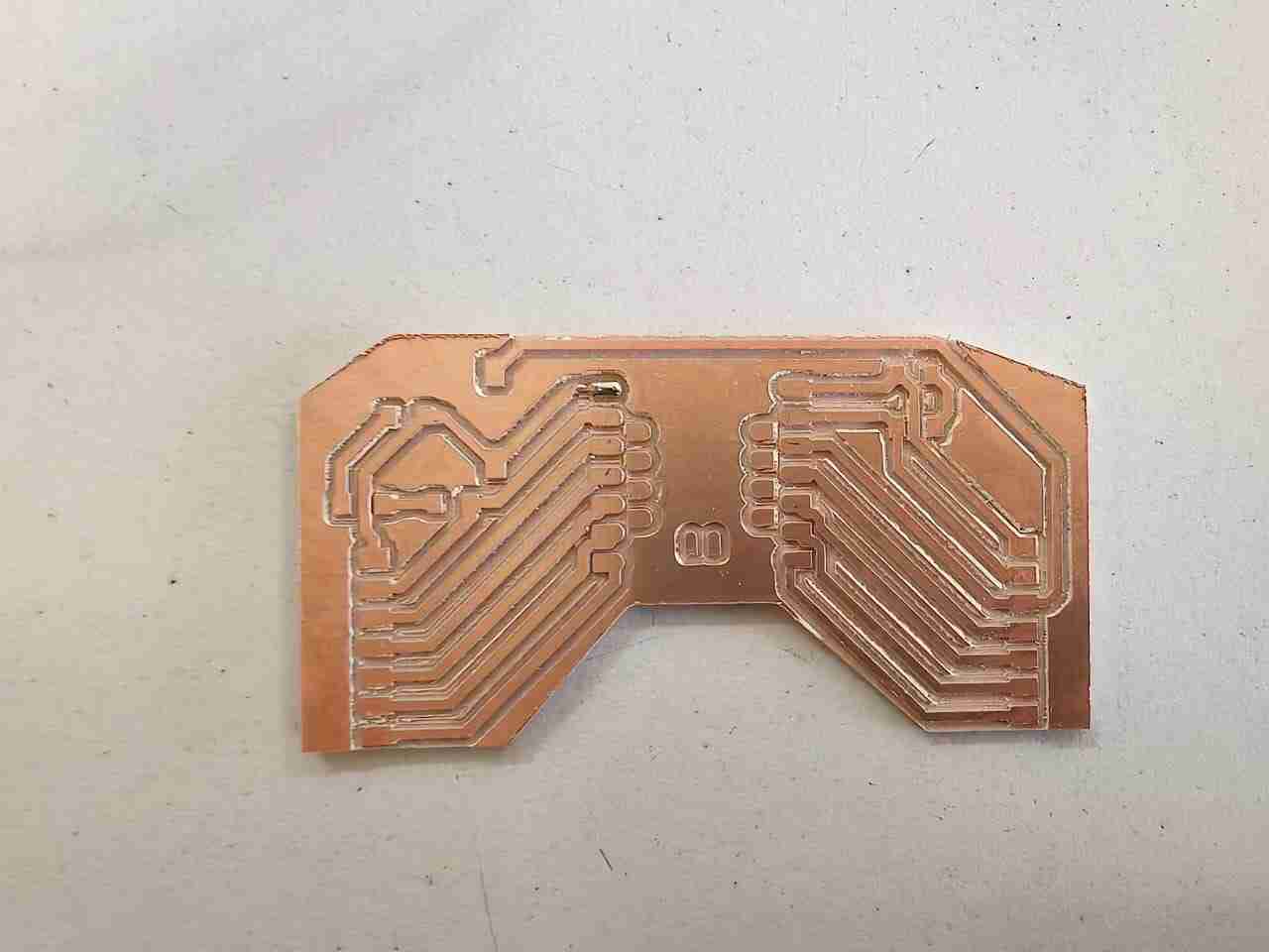
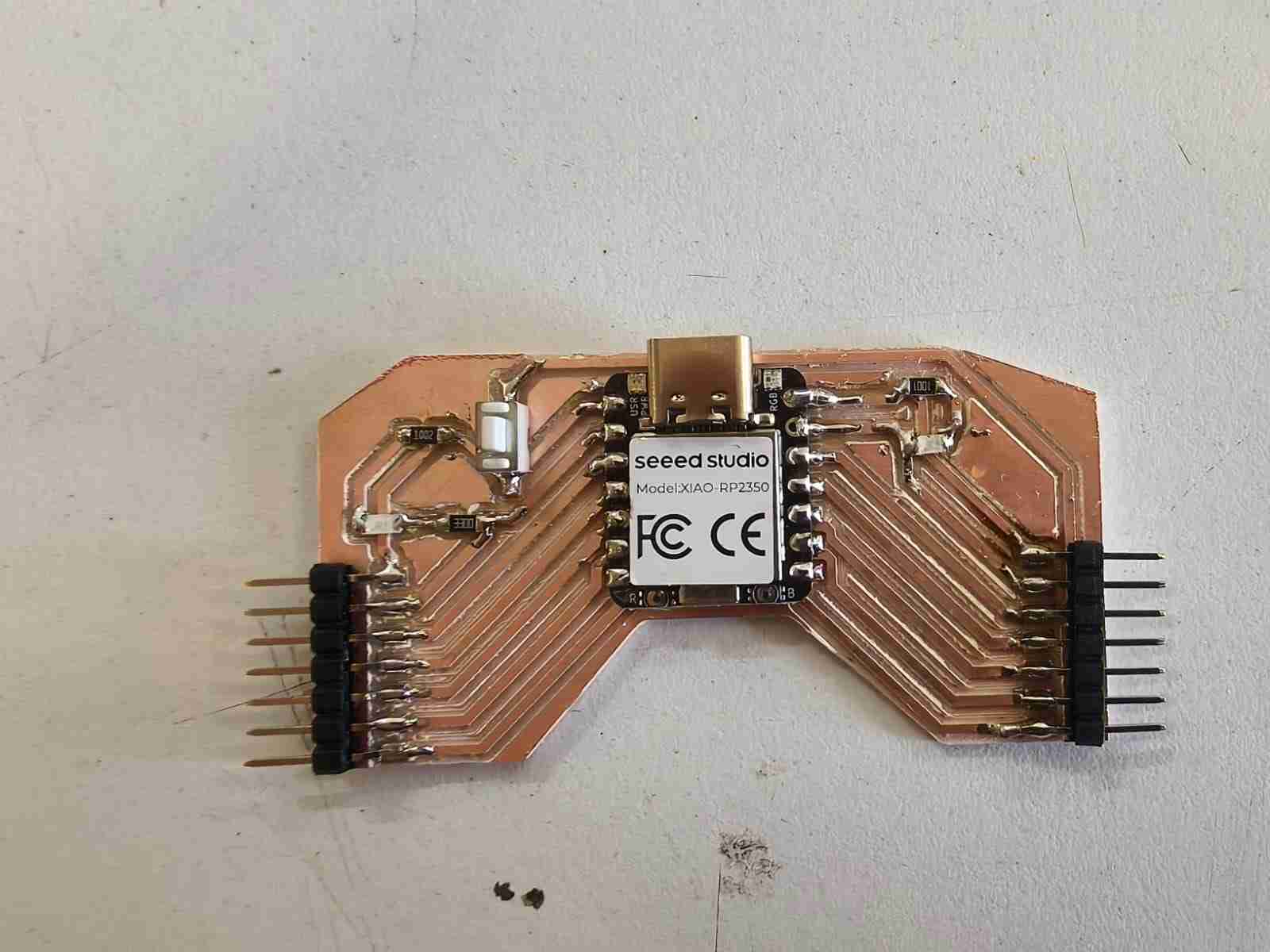
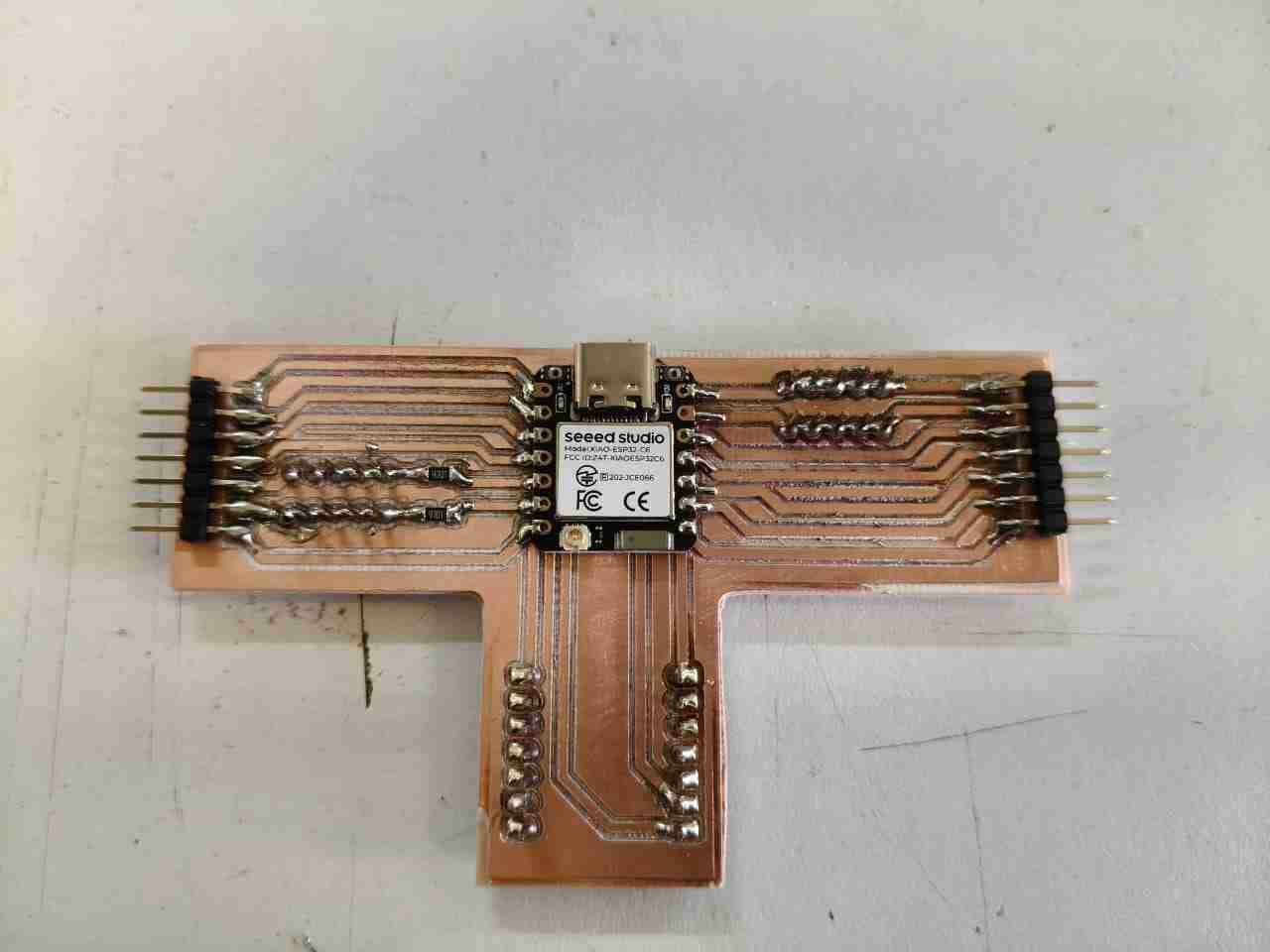
For this week's assignment, I selected a Xiao RP2350 board provided by our local instructor as the base component for my PCB. Although I plan to use a Raspberry Pi Pico 2 for my final project, the RP2350 chip in the Xiao form factor will be useful for testing electronics, sensors, and actuators before finalizing my choice of the Raspberry Pi Pico 2 board. I designed the board as a single-layer PCB, as I had a sufficient supply of SMD components, such as resistors, buttons, and pin headers, which enabled me to avoid using through-hole components. This board features a push button and two LEDs: one that lights up whenever the PCB is powered and another connected to a GPIO from the Xiao board for debugging purposes. Week 6 assignment .
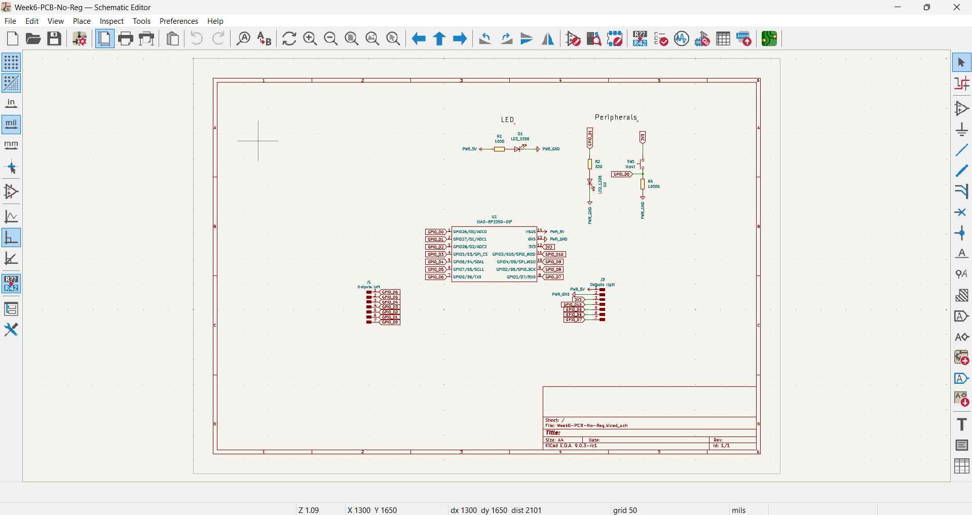
As per my instructor's advice, I decided to use an irregular shape as the outline for my PCB instead of rectangles or squares. This choice helped me better understand how KiCAD can create odd shapes, which could later be transformed into functional designs for encasing electronics.
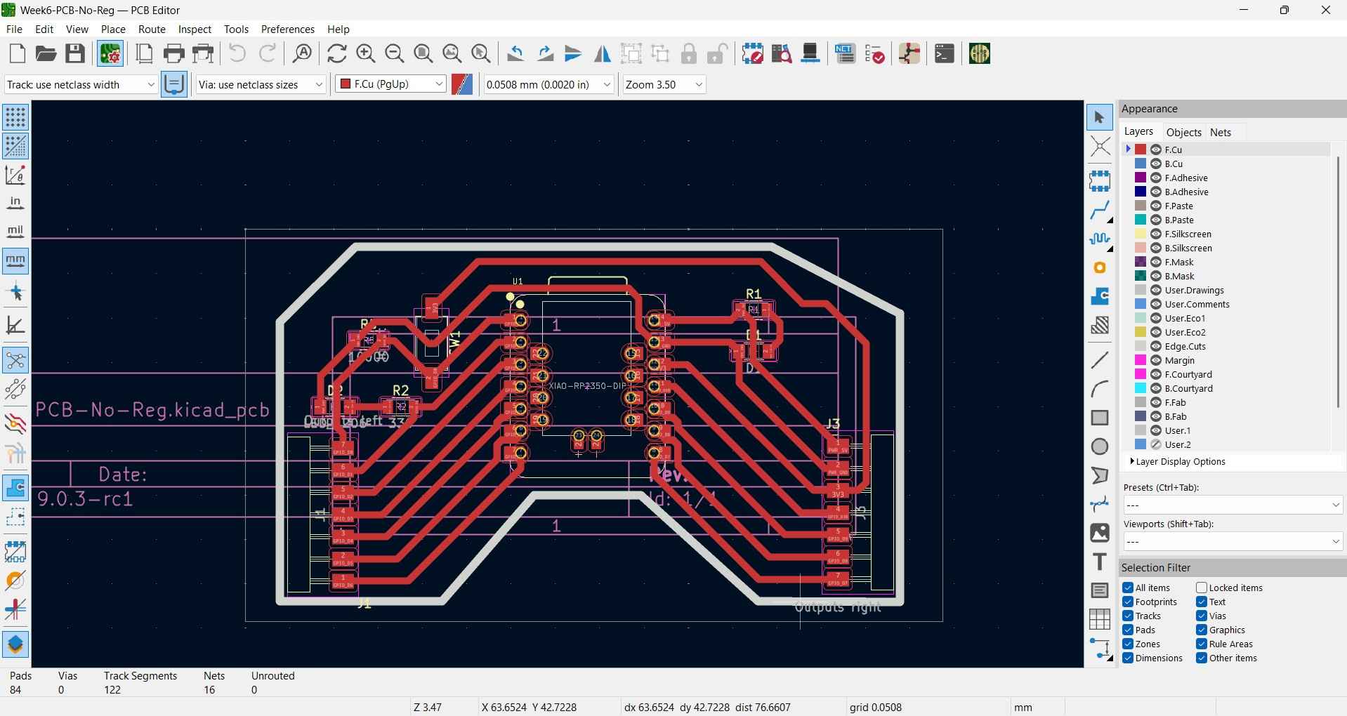
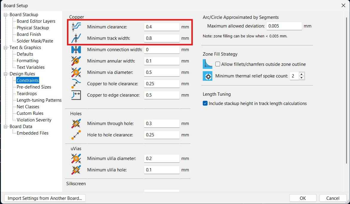
An important step is ensuring that track width and clearance are within the specifications of the available hardware. I have heard stories of individuals who have successfully milled tracks with a width of 0.4 mm and a clearance of 0.4 mm. While this achievement is impressive, I did not consider those metrics necessary for my design. Therefore, I decided to stick with the standard track width of 0.8 mm and a minimum clearance of 0.4 mm, as recommended for the Roland monoFab SRM-20 machine.
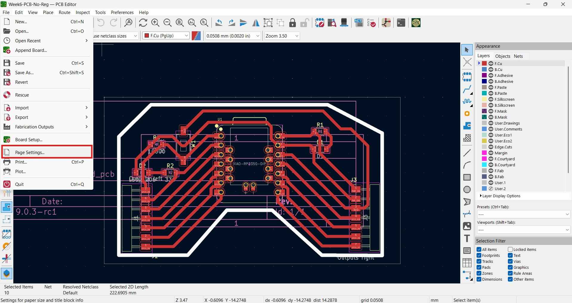
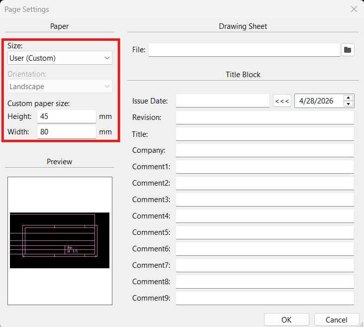
Before generating the manufacturing files, ensure that you plot them in an area slightly larger than the surface of your design. If we neglect this aspect, the spindle of the milling machine could miss the optimal starting point, potentially ruining our milling process. To ensure our design is plotted in the correct area, we first have to access the "Page settings" menu under the "File" tab.
To input specific measurements, first select the User (Custom) option under the Size menu. Then, manually type in the desired height and width before clicking OK to make the changes effective.
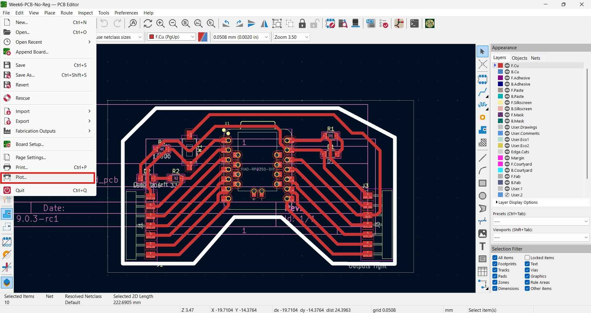
After changing the page size, you may need to reposition the PCB (printed circuit board) outline within the page boundaries. This can be done easily by selecting all elements of the design and moving them with your mouse. Once the design is correctly positioned, you can start generating the manufacturing files by accessing the "Plot" menu under the "File" tab.
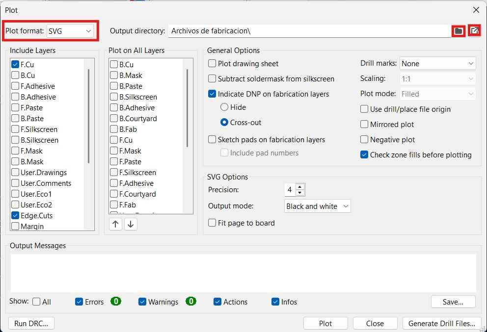
Once the "Plot" menu opens, we must first select "SVG" as our "Plot format" choice and include all the layers from our file that contain elements we wish to mill on our phenolic board. After clicking the "Plot" control at the bottom of the window, we can access the generated files by clicking the arrow located at the top left corner of the window. Next to this button, we can also find an option to choose another folder for saving our output files.
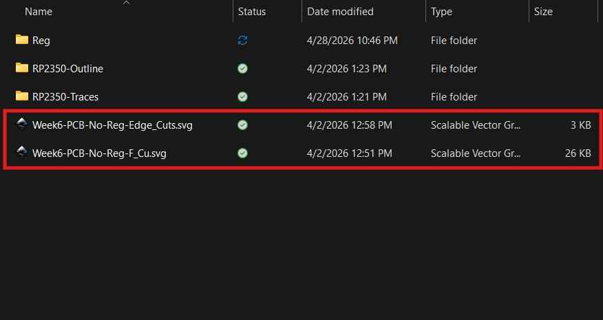
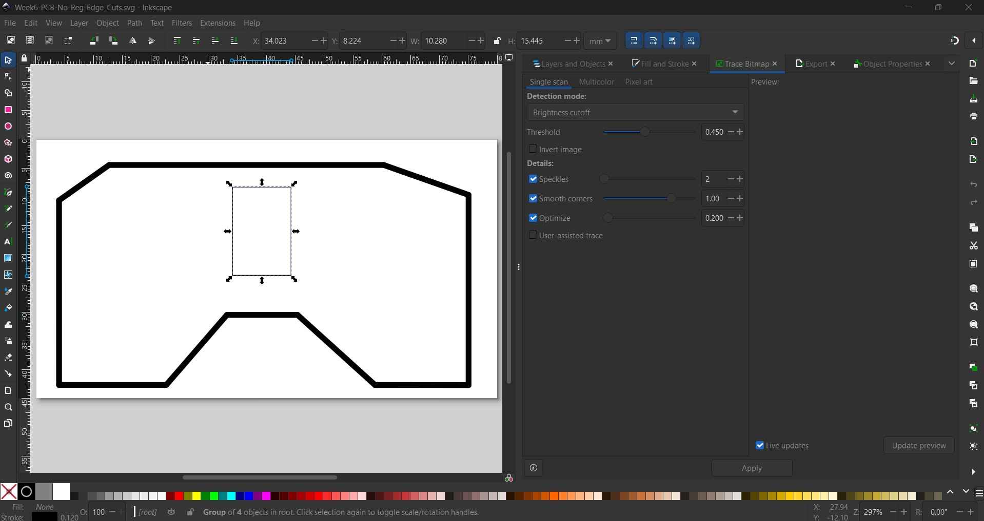
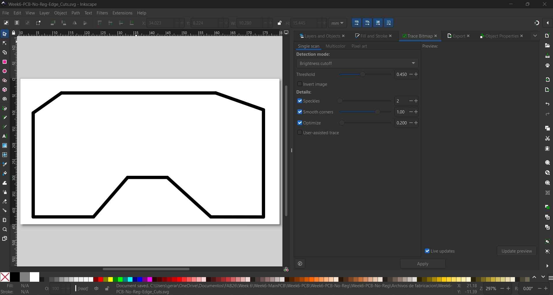
The manufacturing files were exported in SVG format, enabling us to review them in software like Inkscape. This is helpful for confirming that the components of each layer are of the intended dimensions and are distributed correctly. In my case, the footprint for the Xiao RP2350 includes a rectangle for reference when designing around this microcontroller. However, this rectangle represents additional traces for the milling process, so I deleted it from the design using Inkscape. This change will be noticeable when drafting milling trajectories.
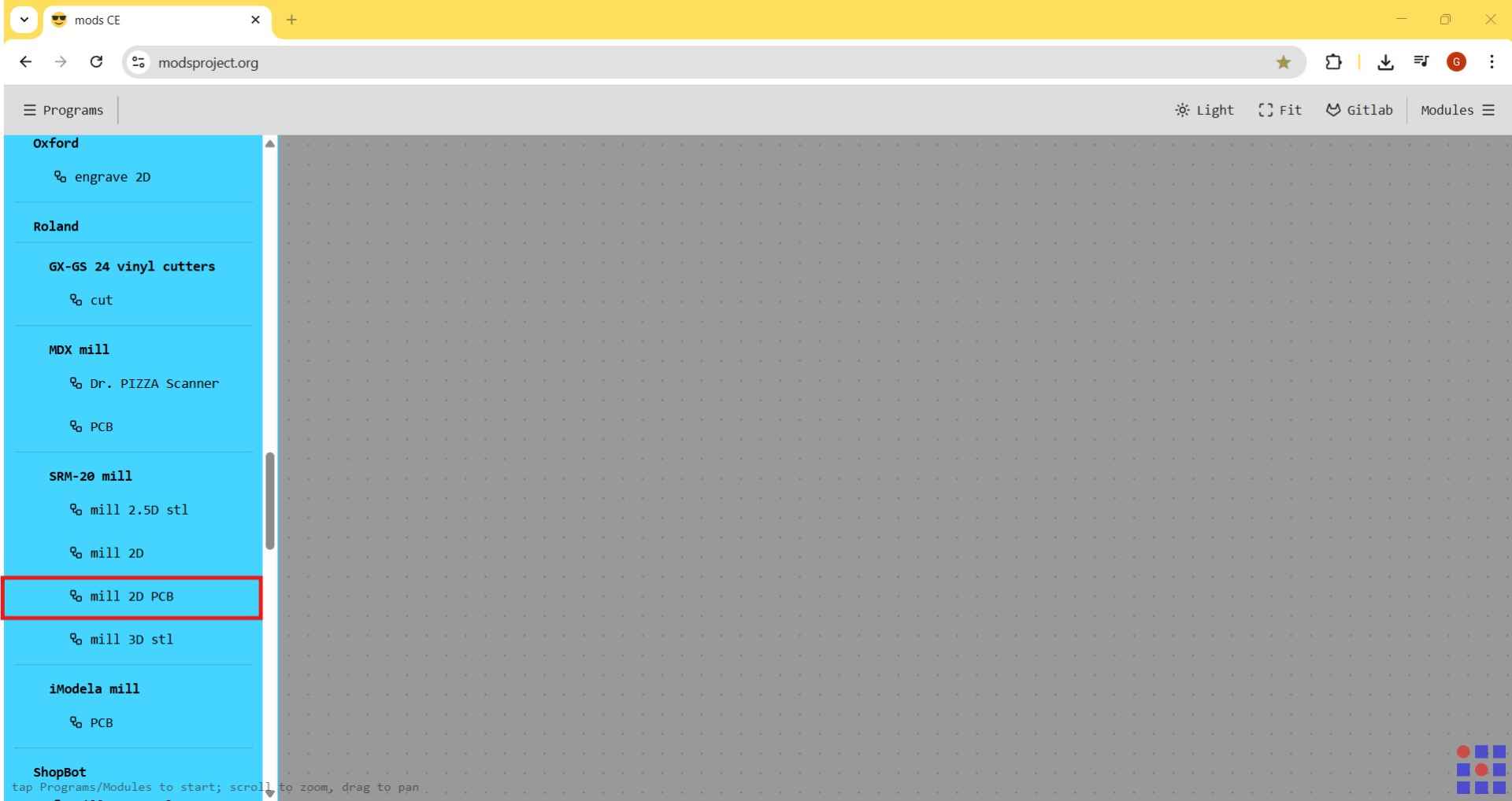
3. Roland monoFab SRM-20
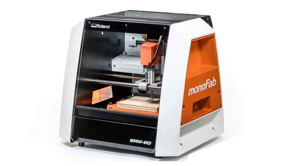
The Roland monoFab SRM-20 is a compact CNC milling machine for desktop use, primarily designed for prototyping, engraving, PCB milling, creating wax molds, producing acrylic parts, crafting foam models, and fabricating small plastic components. It serves as a precision prototyping mill rather than a heavy-duty metal-cutting CNC machine. For PCB isolation, it is frequently utilized in FabLab environments for detailed PCB milling. Its main advantage lies in its built-in enclosure, which effectively contains waste dust, vibration, and sound during the milling process.
3.1. mods CE
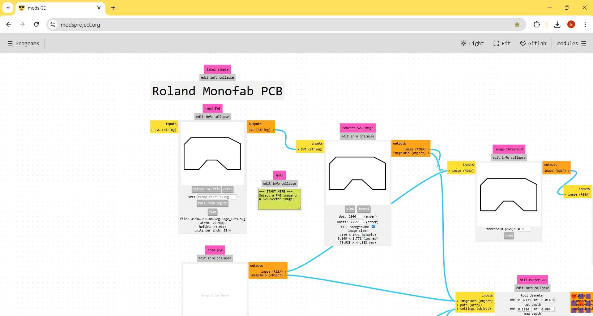
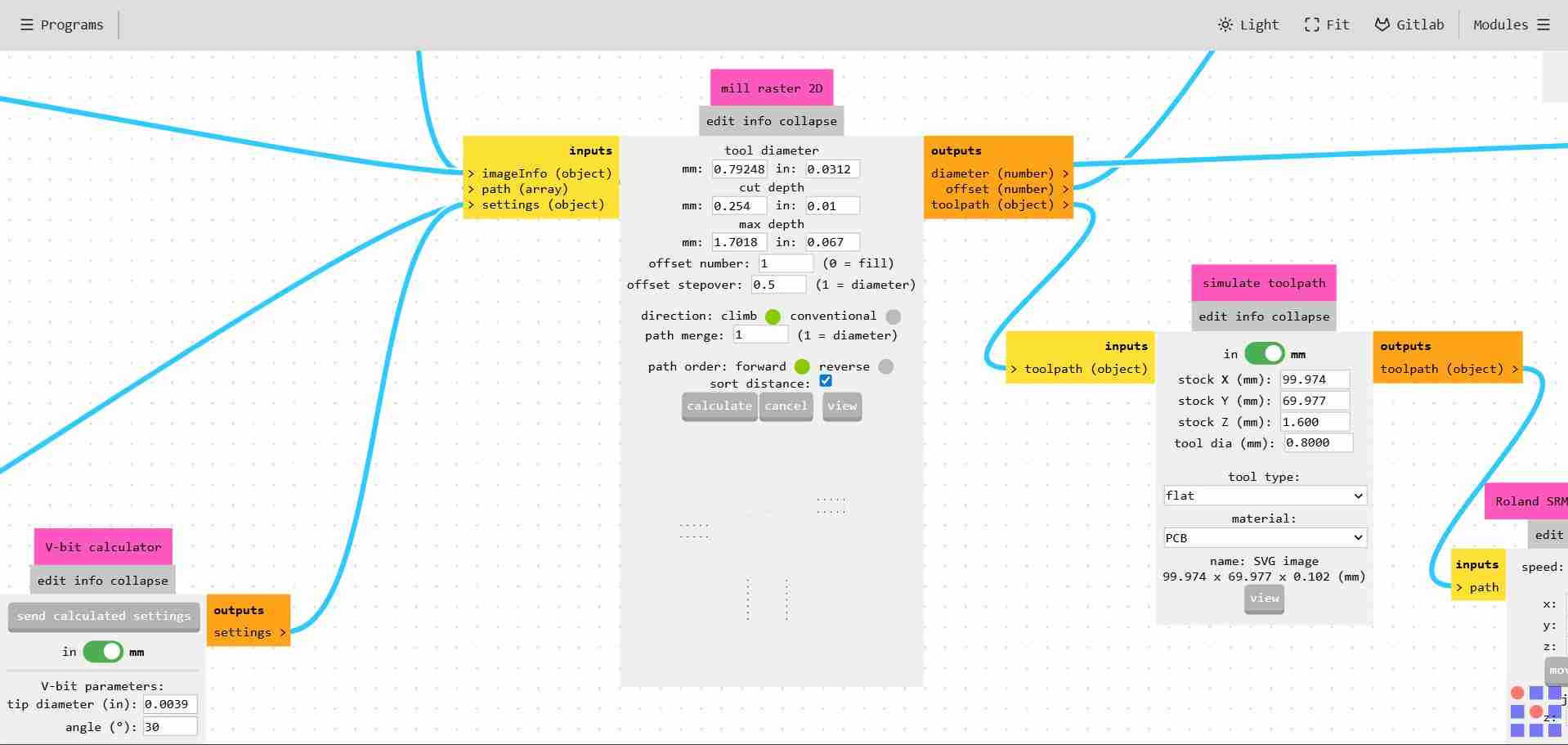
Mods CE is a browser-based, modular CAM/control environment utilized in FabLabs for digital fabrication machines, including CNC mills such as the Roland SRM-20. It converts design files into machine instructions. For CNC PCB milling, Mods CE can process a PNG trace image, calculate the toolpath, and generate output files in formats compatible with machines like the Roland SRM-20 or those from the CNC3018 family.
To generate the toolpaths, we must first access the Programs menu after entering the codes. When the menu is opened, it will display various programs designed for different applications and tailored for specific machines.
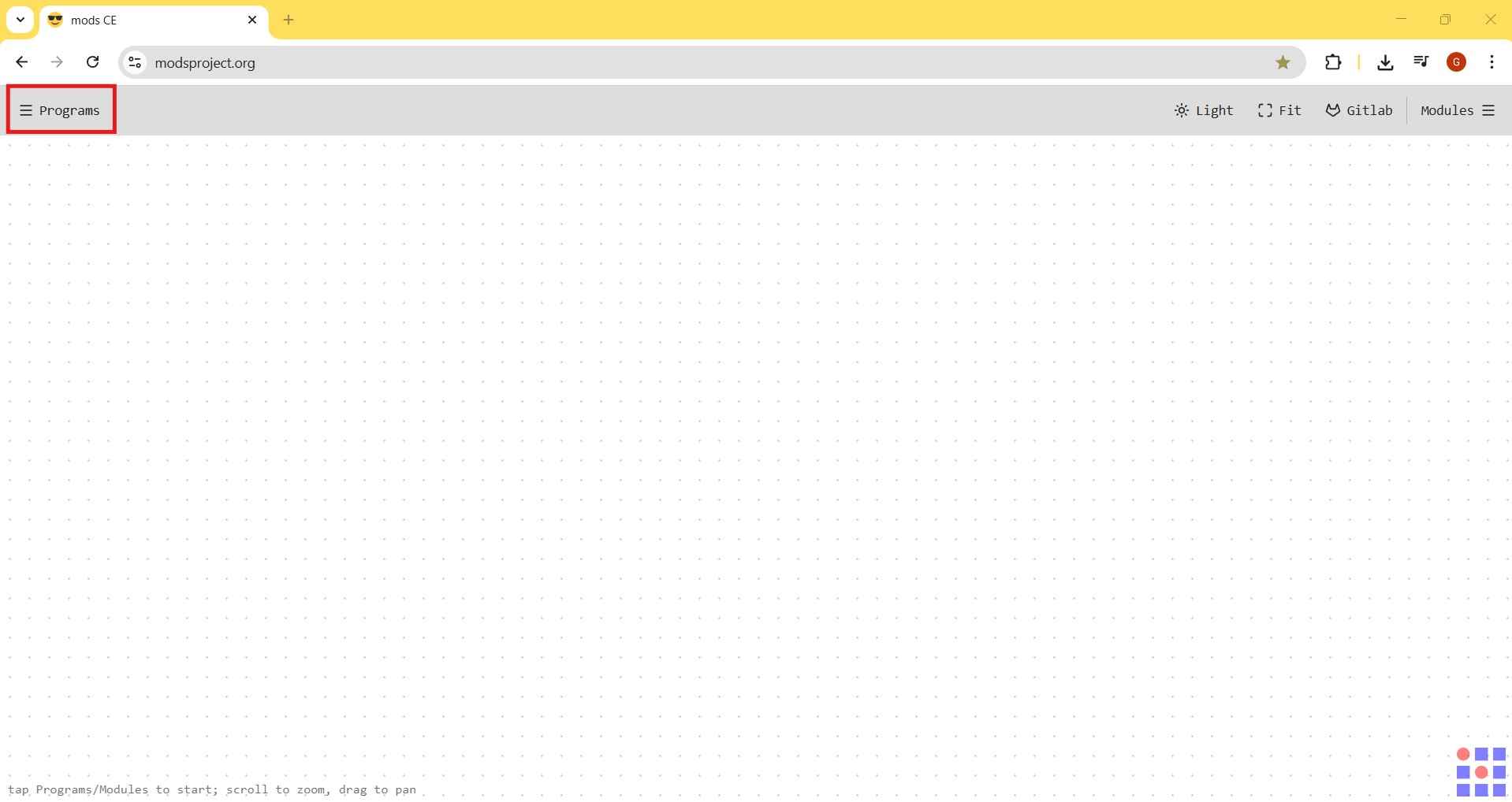
From the menu, select mill 2D PCB under the SRM-20 mill category.
After selecting the SRM-20 mill option, mods CE will display the framework that is ready to receive files for toolpath generation. Users can navigate this framework by clicking anywhere on the white background with the left mouse button and dragging the mouse.
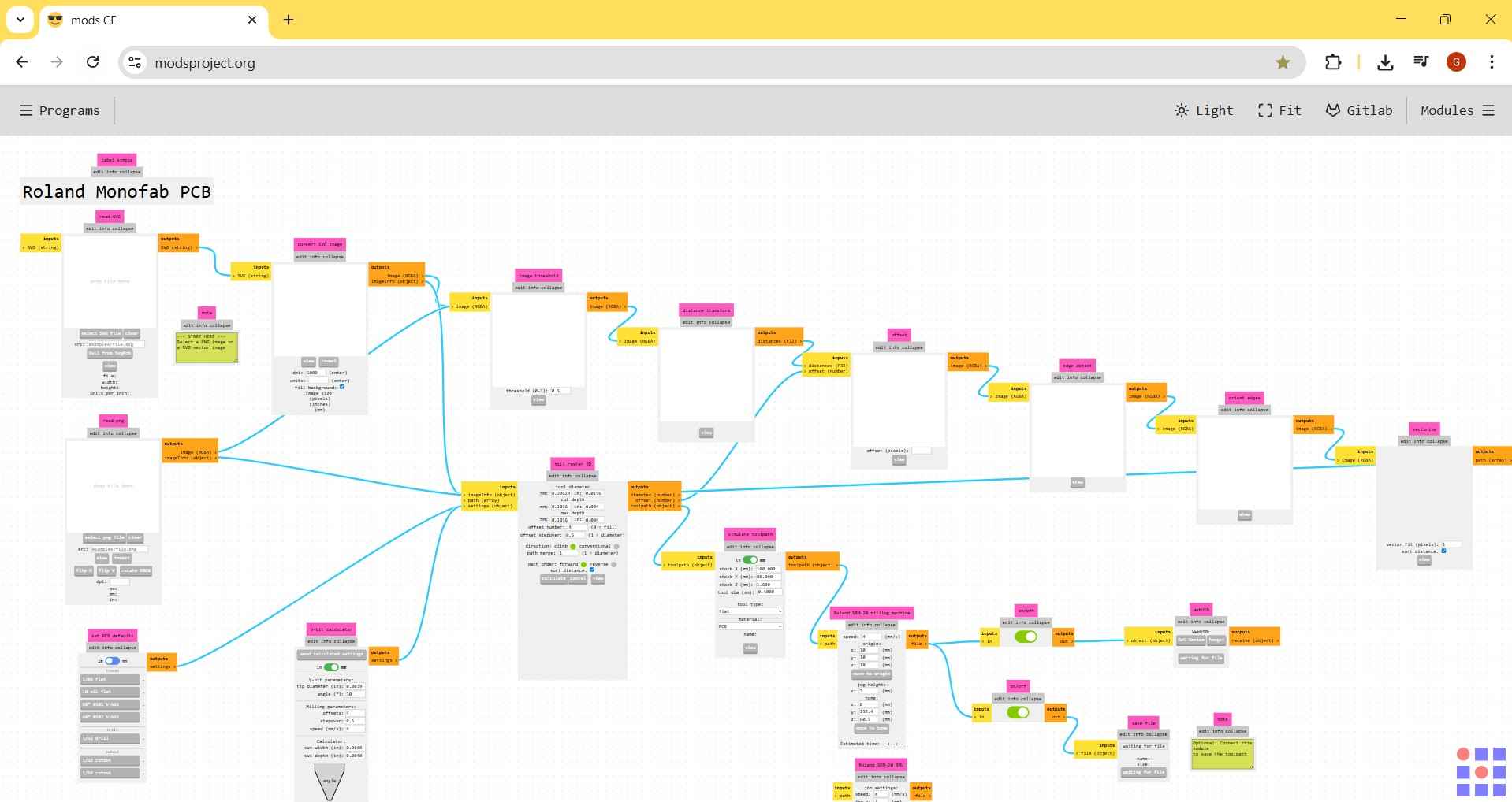
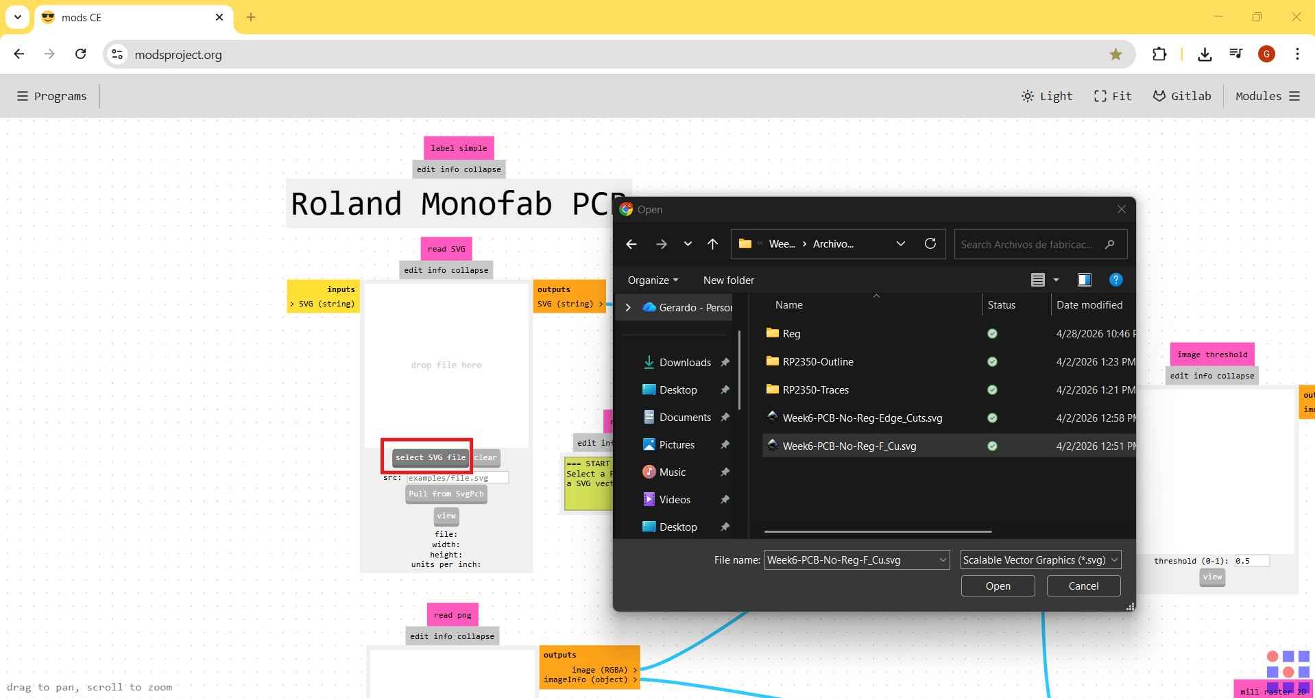
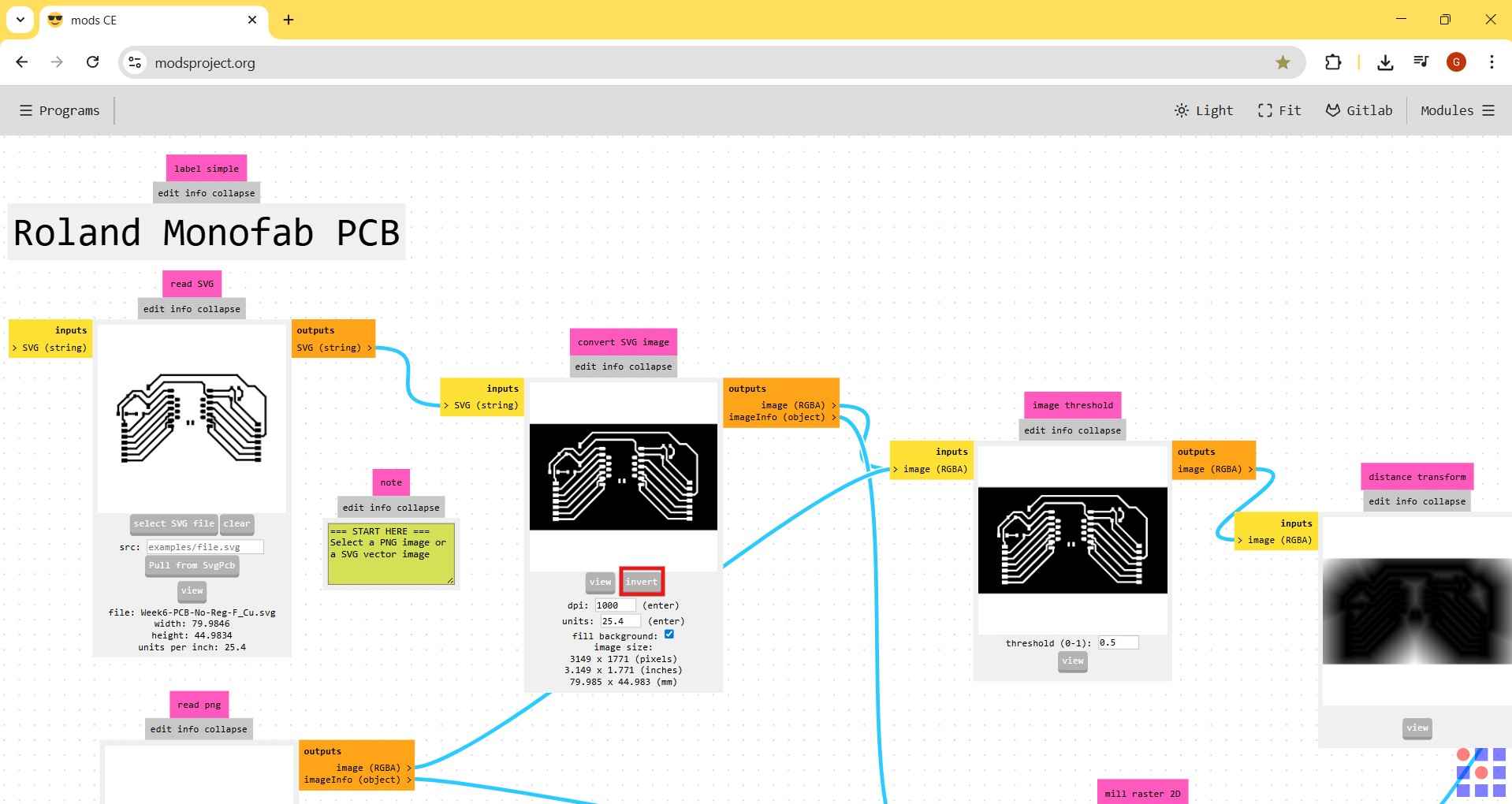
Toolpath generation begins by selecting our SVG files in the read SVG module.
After selecting an SVG, the framework should display an image similar to what is seen in KiCAD or Inkscape. The read SVG module also provides relevant information, such as the height and width of the selected SVG. It is important to note that the black outline of the image indicates the areas that will define the machine toolpath.
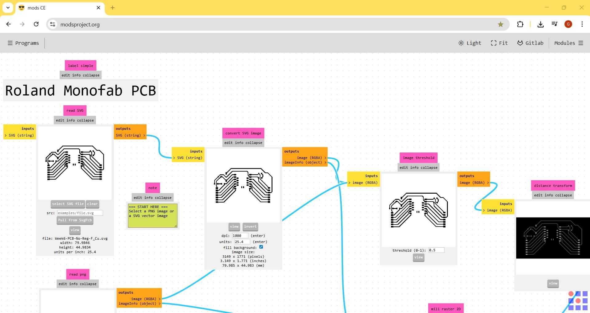
When drafting the traces outline, it is essential to click on "invert" in the convert SVG image module to accurately create the silhouette of the circuit traces. If you overlook this step, the CNC will position its spindle over the intended traces instead of around them. This error would lead to the removal of a shape resembling the traces, rather than isolating them.
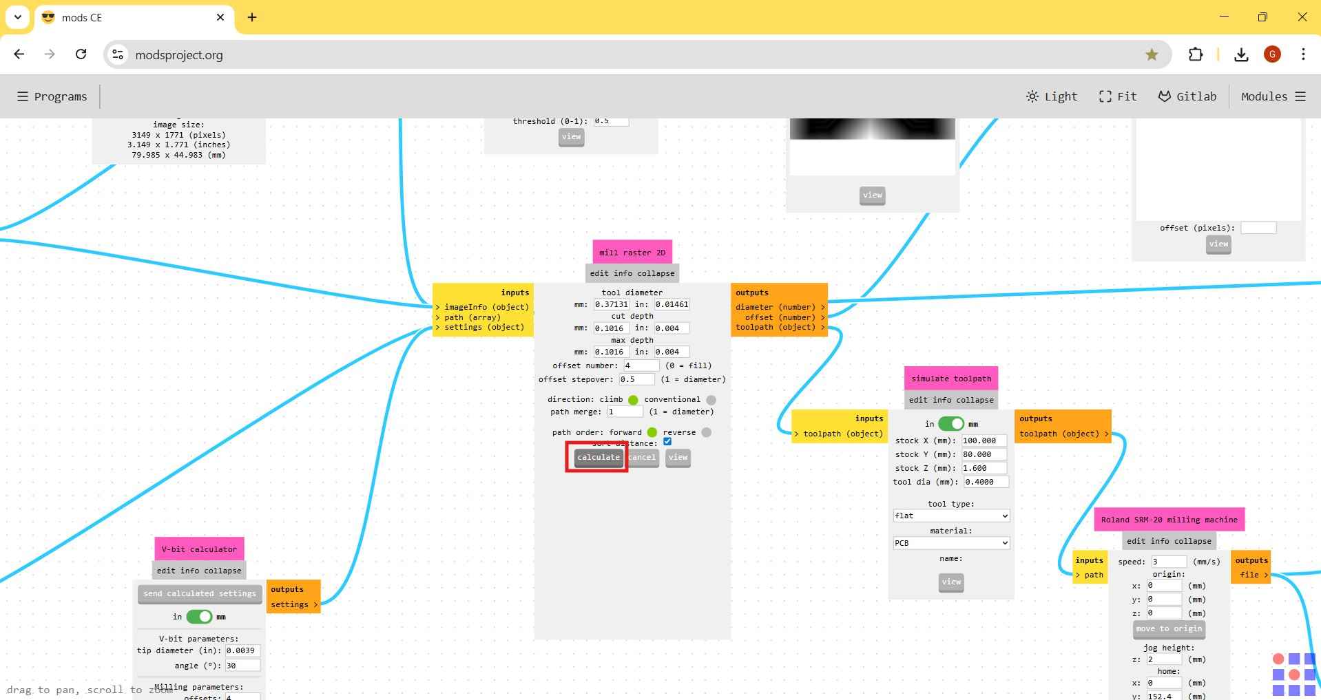
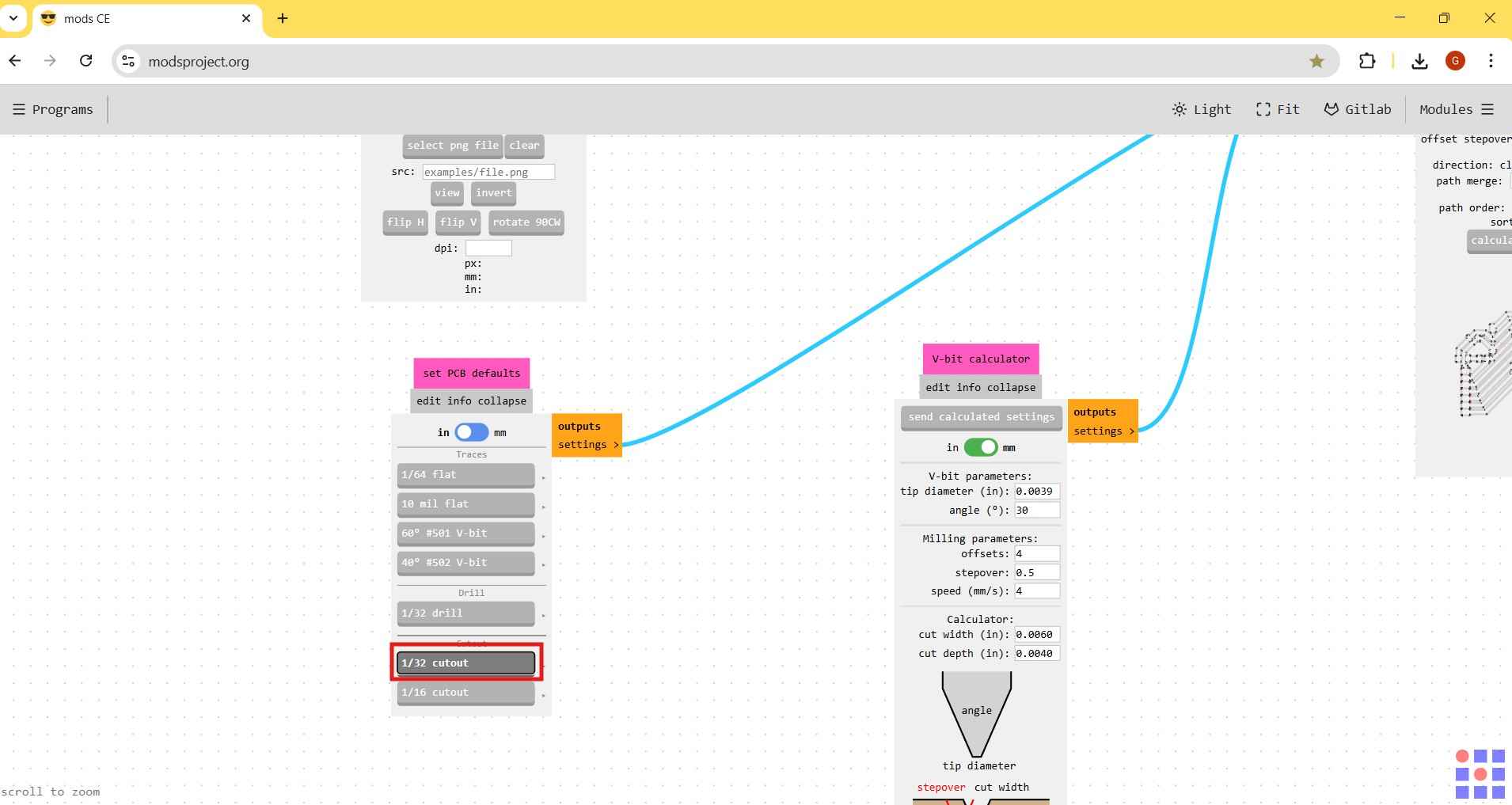
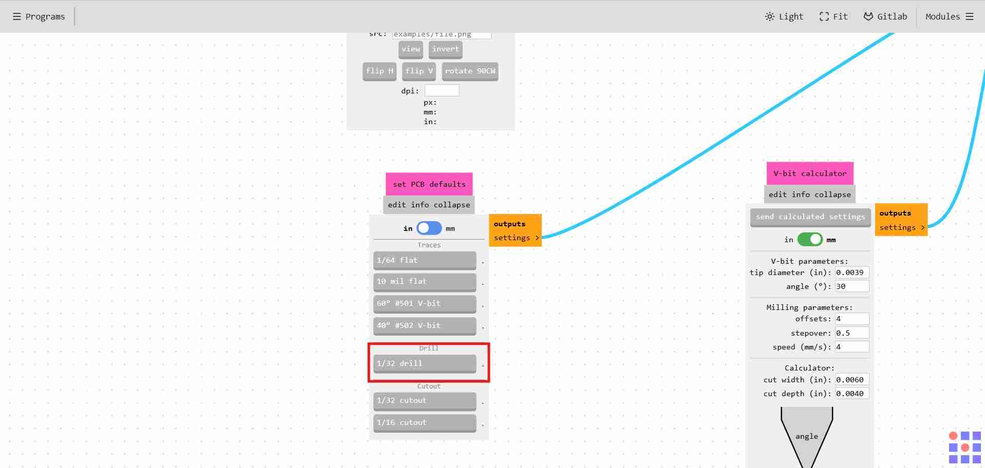
Our FabLab is equipped with 0.1 mm V-tools featuring a 60-degree sharp angle. This tool option is available in mods CE and must be selected to proceed with toolpath generation.
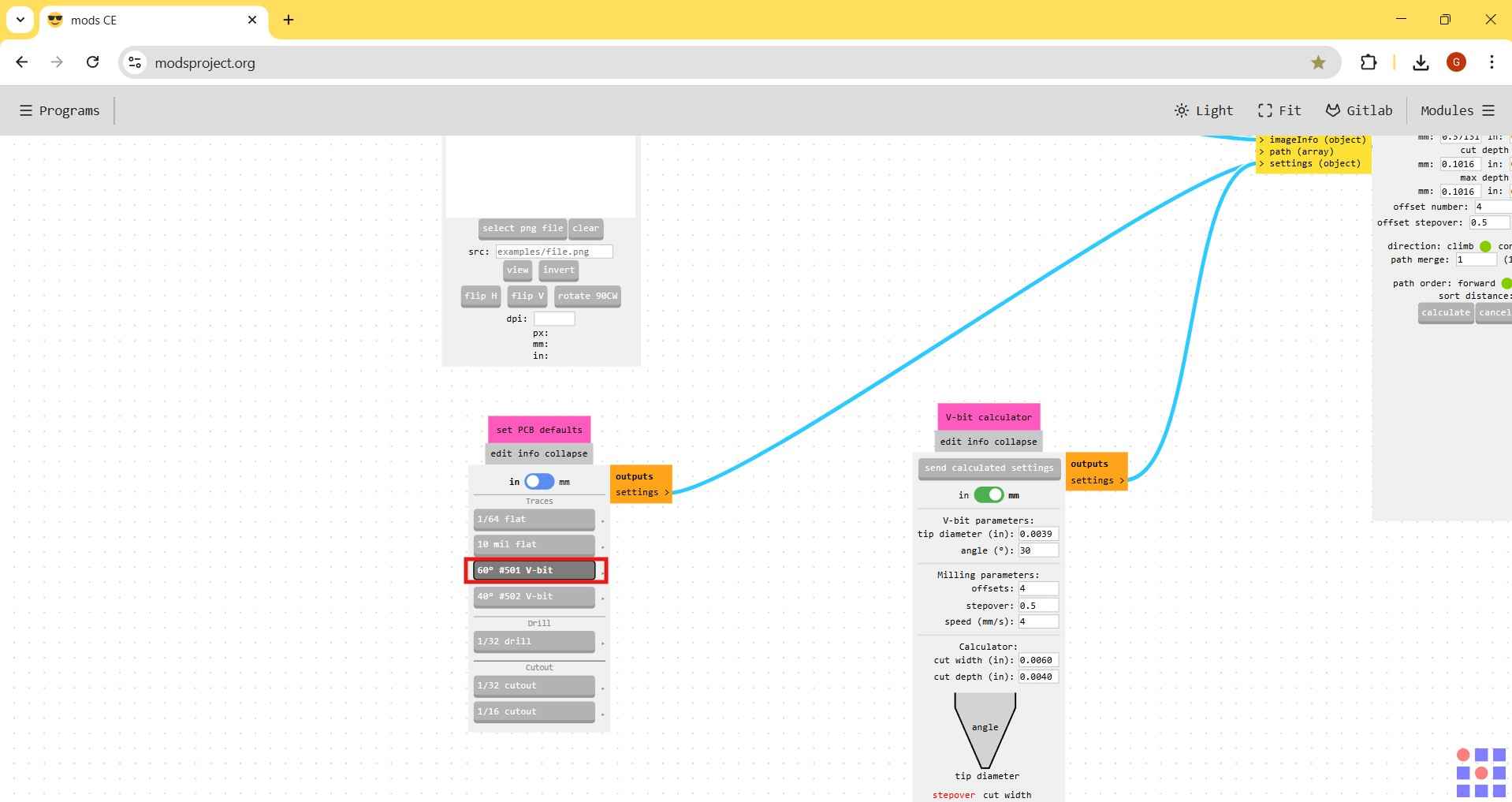
The speed at which the spindle moves is a crucial factor that influences whether a tool will break or produce the desired milling result. In this mods CE program, the speed can be adjusted using the Roland SRM-20 milling machine module. For the V-tool mentioned earlier, I recommend reducing the speed from 4 mm/s to 3 mm/s. Additionally, it is essential to set the origin to zero on the X, Y, and Z axes; otherwise, the milling process will begin at an incorrect offset. I also suggest pressing the "move to origin" button each time a new trajectory is calculated.
Now that the speed is set, let's examine the mill raster 2D module. This is where users can adjust the offset number, cut depth, and tool diameter. The tool diameter does not need to be modified since it has already been selected. The same applies to the cut depth and maximum depth, as both are set to the same value. The tool does not need to penetrate the entire phenolic plate because this path is intended for PCB trace isolation. The copper layer is typically only 0.1 mm thick, making it easy to remove with a single pass of the v-tool. The offset number indicates how many times the machine will move in the same direction. Repetition helps prevent traces from touching due to residual copper dust, but excessive passes could disrupt properly functioning traces. For this PCB, the optimal number of repetitions is four. With all parameters set to the desired values, we can click "calculate" to generate the milling trajectory for our PCB traces.
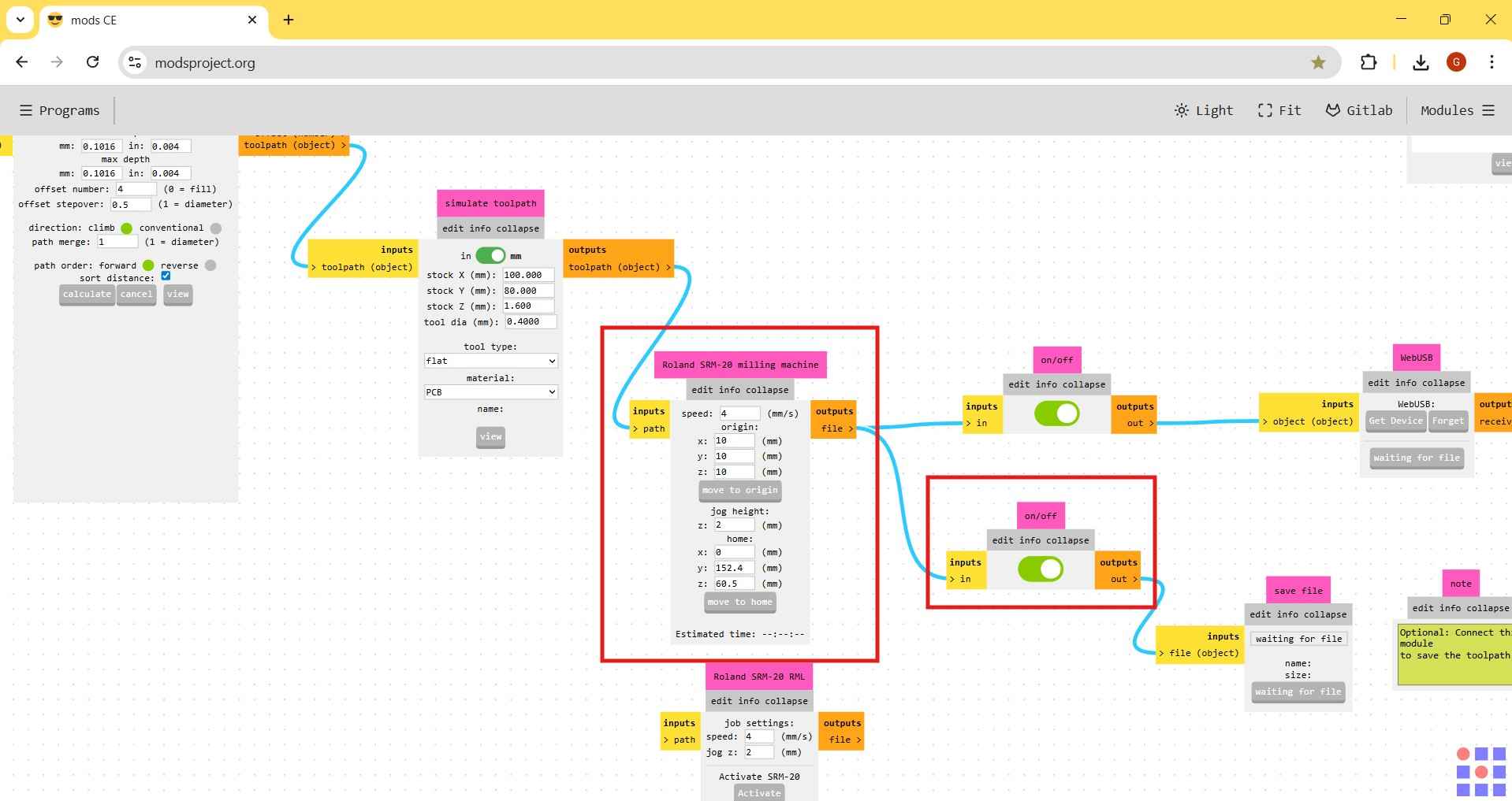
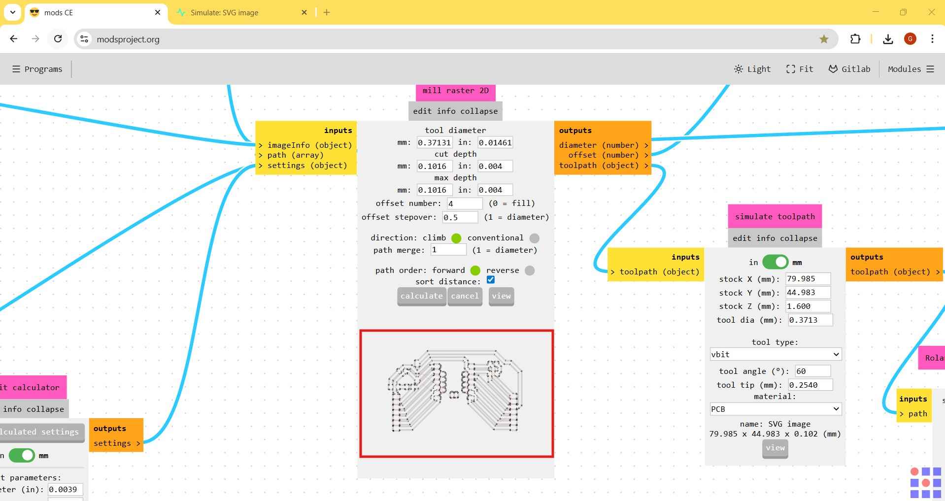
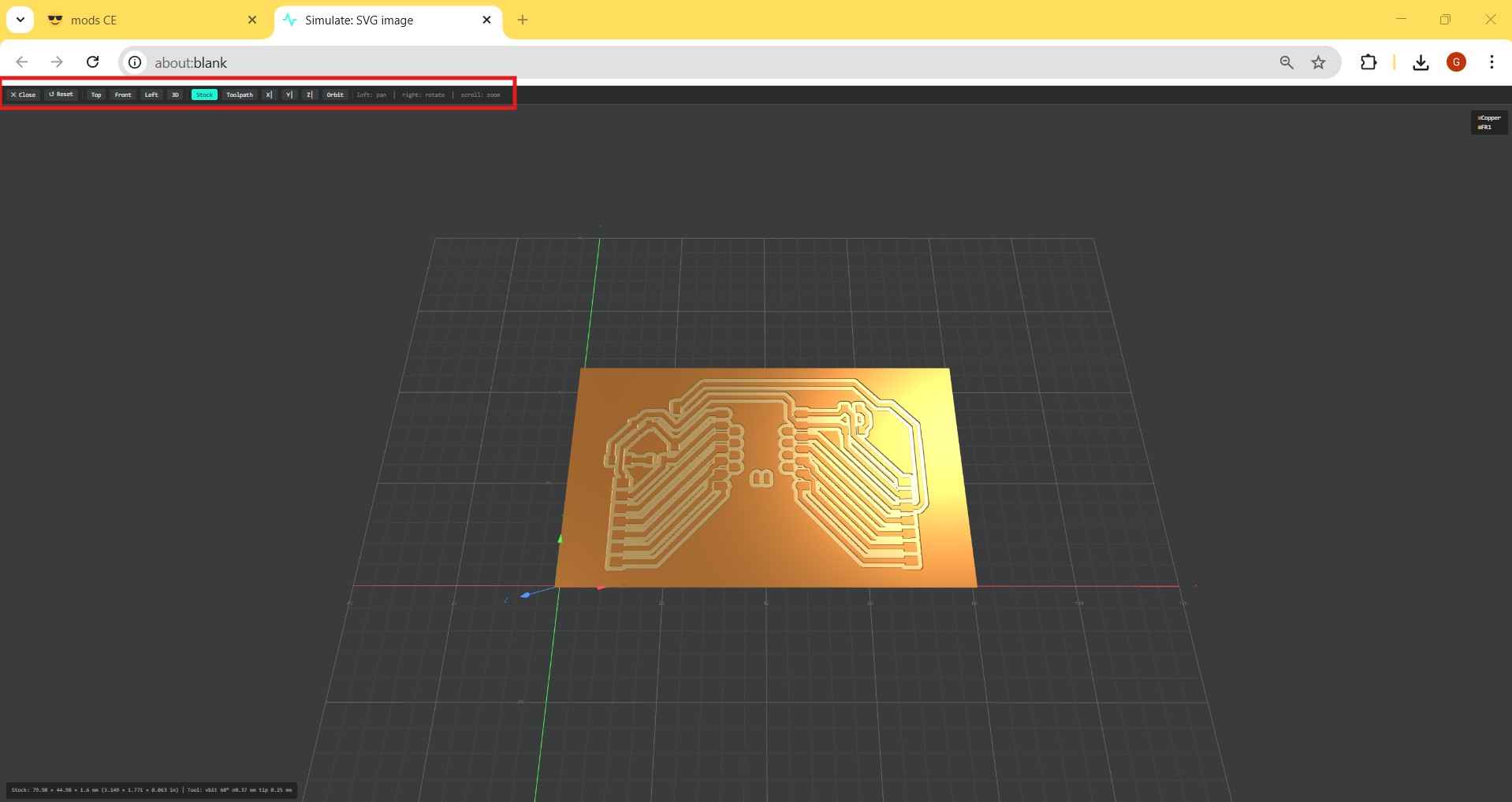
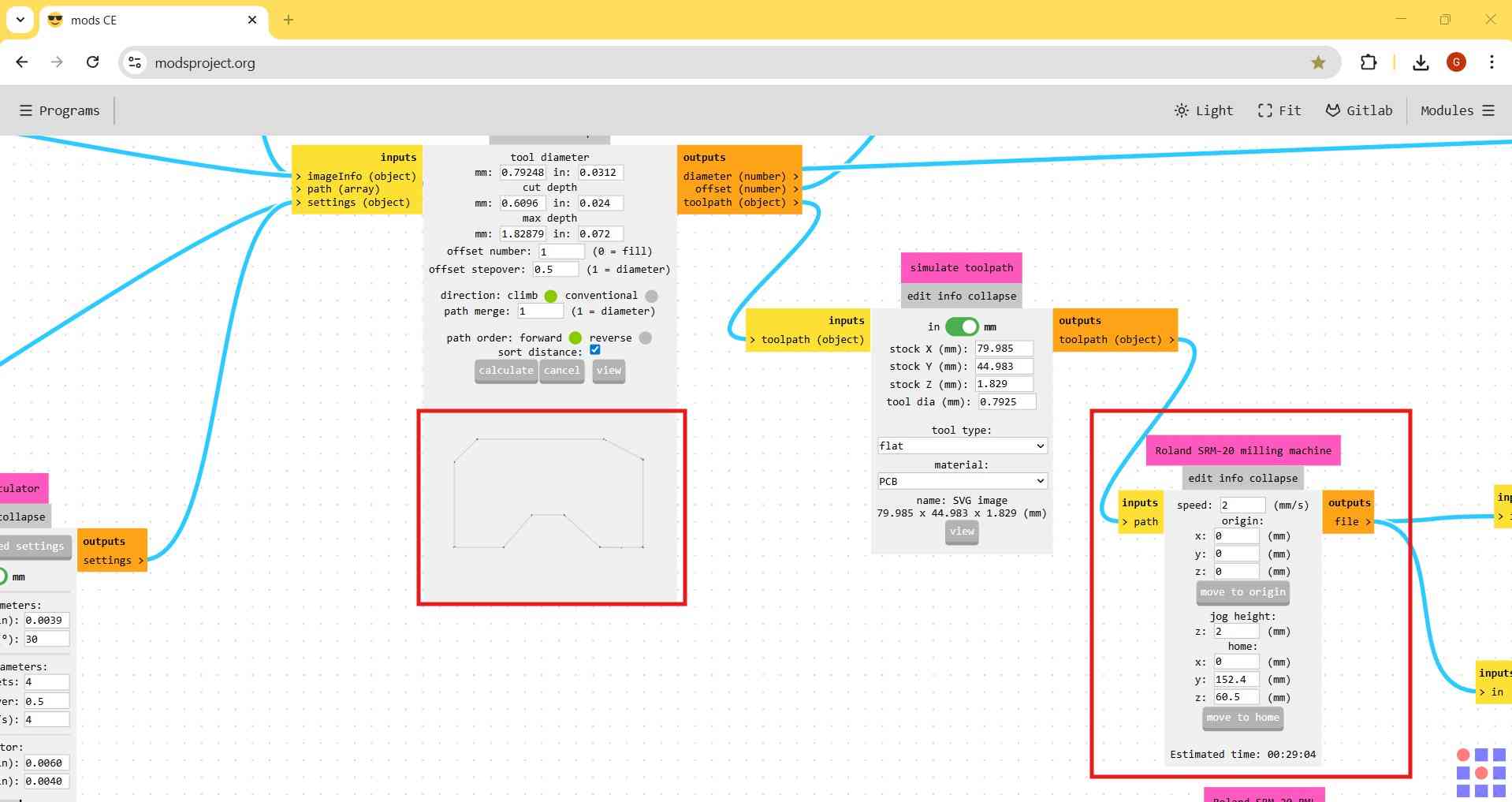
After the calculations are complete, the module will display the trajectory of our PCB traces. A window will automatically pop up, showing a 3D render of the PCB traces. This window includes additional buttons for controlling display options.
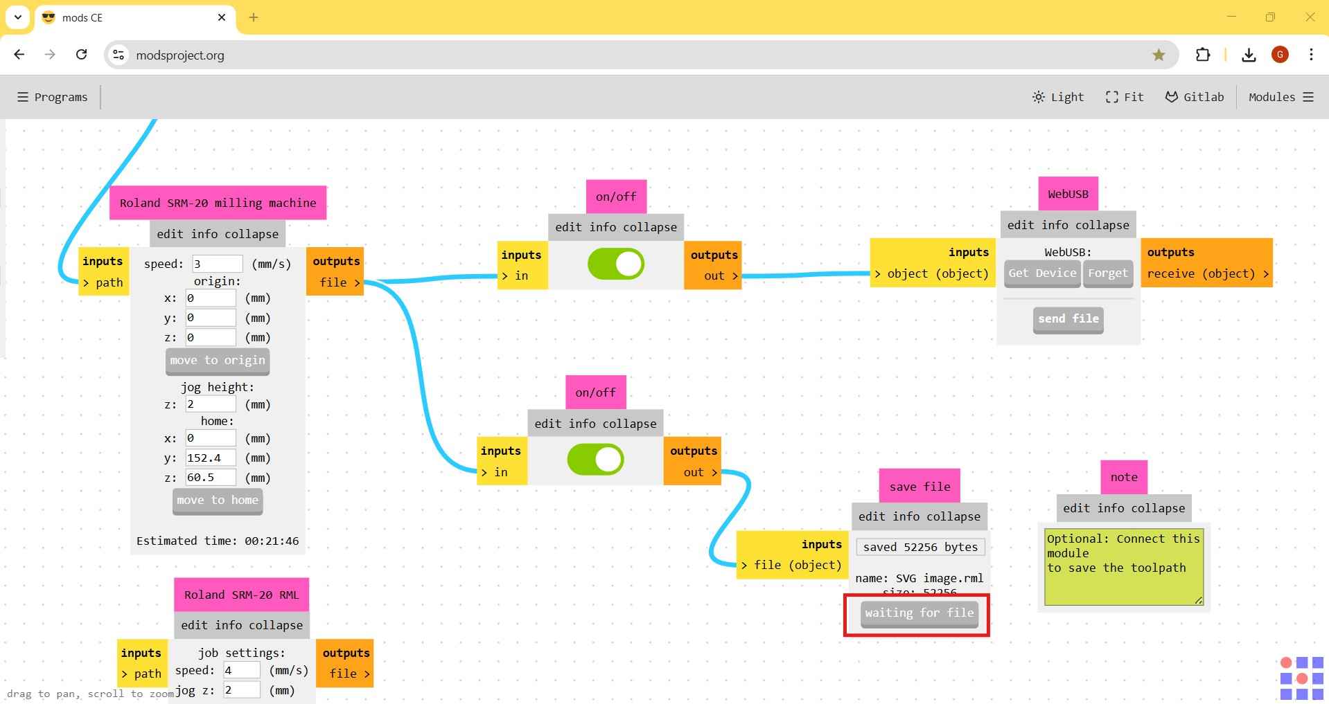
After visually validating the generated trajectory, you can download the file containing the trajectory instructions by pressing the "waiting for file" button in the save file module.
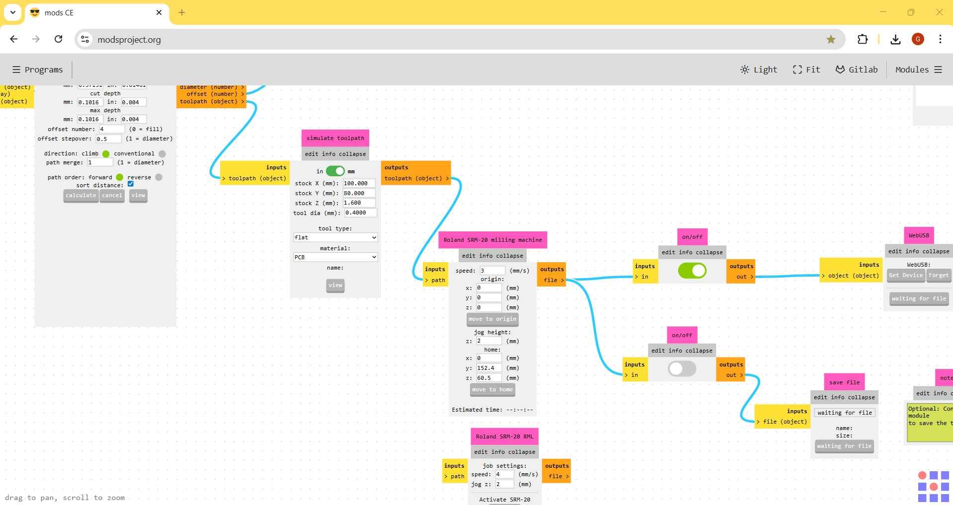
The workflow for the PCB outline is similar to the one previously described for the traces, but with a few changes.
The first aspect to consider is the selection of the tool. This part was confusing for me at first because I attempted to design my PCB outline in KiCAD with a 2 mm thickness; however, this value was rejected by modsCE. I decided to switch to a 1 mm outline in my design, which was compatible with modsCE. Another point of confusion arose regarding the tool diameter. When I tried to change the tool diameter from 0.79 mm to 2 mm, I realized the adjustment was not possible due to my 1 mm thickness. Therefore, I opted to stick with the tool diameter provided by modsCE. Fortunately, these discrepancies did not affect my end result.
The cut depth and the maximum depth were not the same in this case. The cut depth was set to one-third of the maximum depth. This prevented the milling tool from cutting through the phenolic board all at once, which could have damaged both the tool and its protective layer. When it comes to speed, the diameter of the tool determines how fast the spindle can move during milling. The speed should not be higher than the tool's diameter.
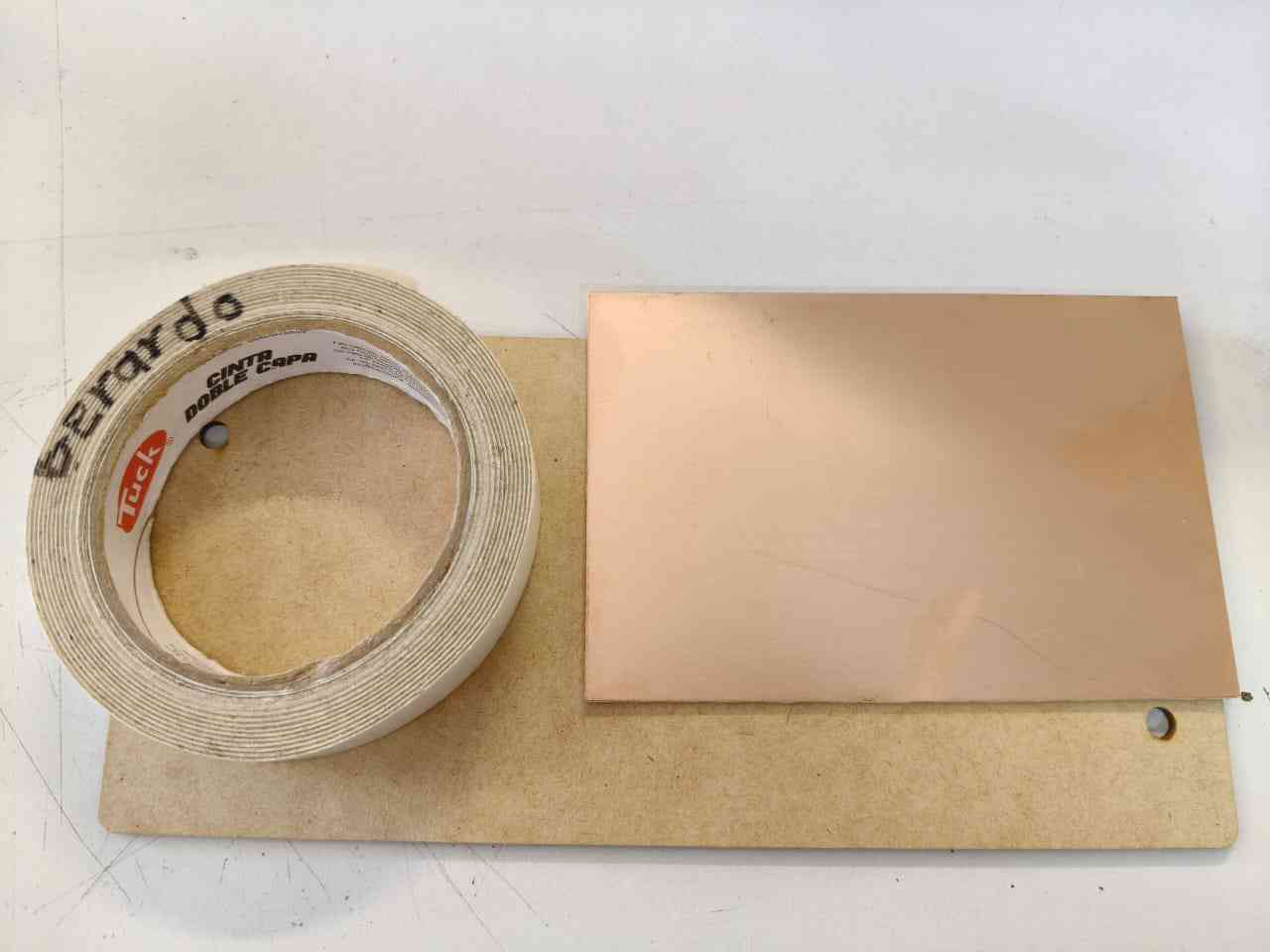
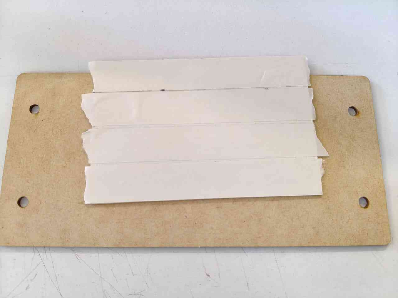
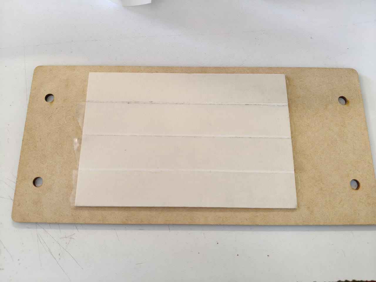
To prepare our phenolic board for the milling process, we will need double-layer adhesive tape and a sacrificial layer; in this case, the sacrificial layer will be an MDF board. A phenolic board can be easily adhered to a sacrificial layer using adhesive tape, provided the phenolic plate is not too curved. I recommend using tweezers to help expose the front face of the adhesive tape if removing it proves difficult.
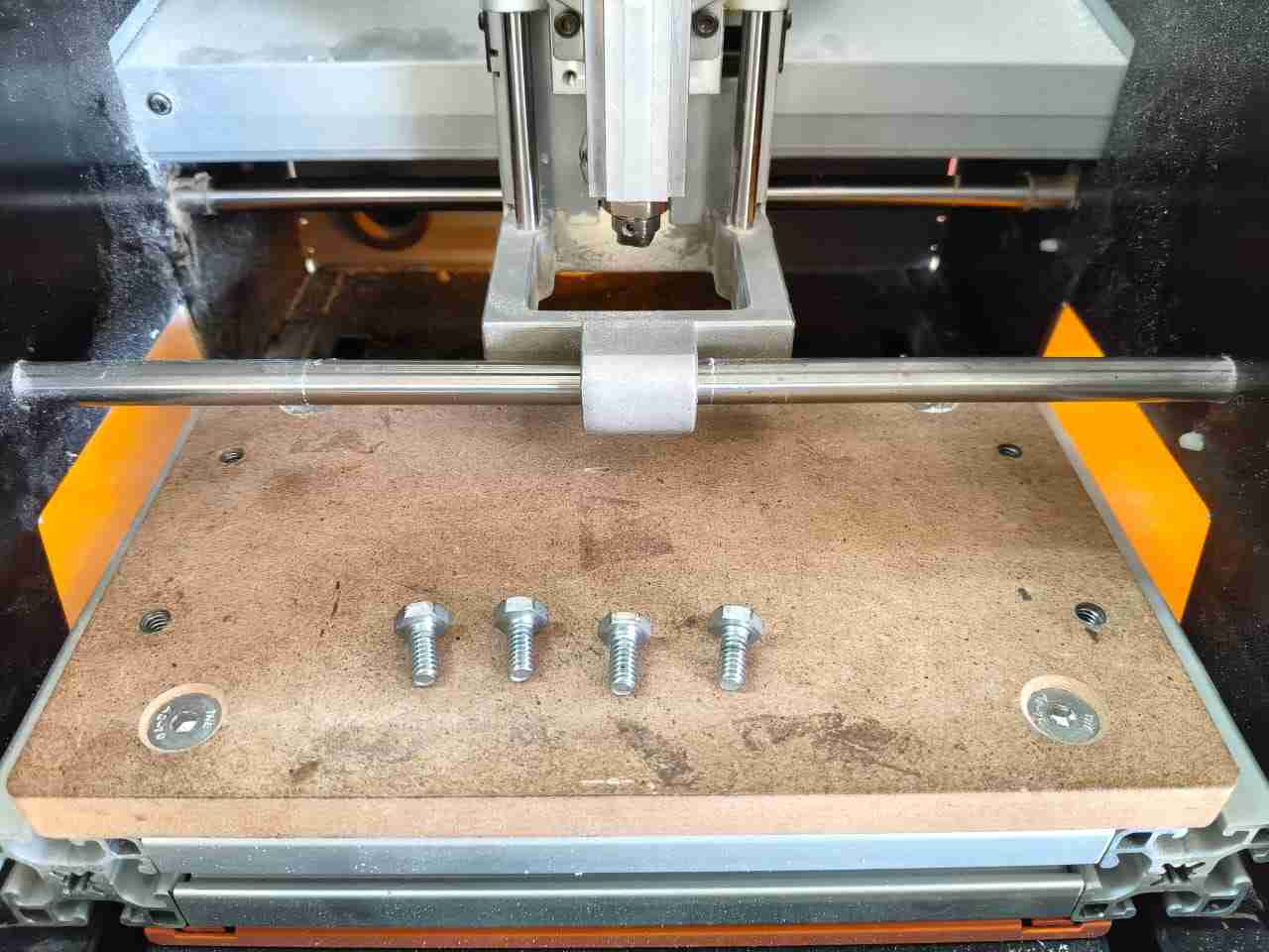
The Roland SRM-20 monoFab machines in my FabLab have been modified with custom beds designed to accommodate sacrificial layers for PCB fabrication. These sacrificial layers are secured in place using four screws, as illustrated in the accompanying picture.
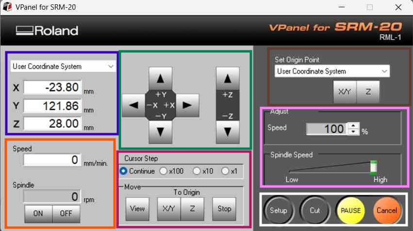
With the phenolic board in place, we can now connect our computer to the monoFab machine. Instructions can be sent to the machine using the V-panel software provided by Roland. I have grouped the controls of the panel based on their functions, which I encased in rectangles for easier identification:
- Blue: The coordinates display section shows the spindle position relative to the origin in the X, Y, and Z axes.
- Orange: The spindle control section is used to manage the spindle's state and speed. The speed is typically set at mods CE, so this section primarily functions to turn the spindle on and off.
- Green: This section controls spindle movement along the X, Y, and Z axes.
- Magenta: The top of this menu includes options for controlling the feedrate of manual spindle movements. Selecting the appropriate feedrate can help facilitate the spindle's placement at the origin. The View button pauses the milling process and moves the bed forward for inspection. The "To Origin" options move the spindle to the stored origin position along the XY plane and the Z axis. The Stop button halts the milling process.
- Brown: The set origin menu; these controls help set the starting point for each milling process.
- Pink: These controls adjust the spindle speed using either a bar control or an arrow box.
- White: These controls can initiate a milling process, load a trajectory file, pause an operation, or cancel the current task.
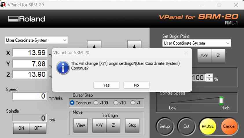
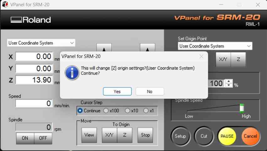
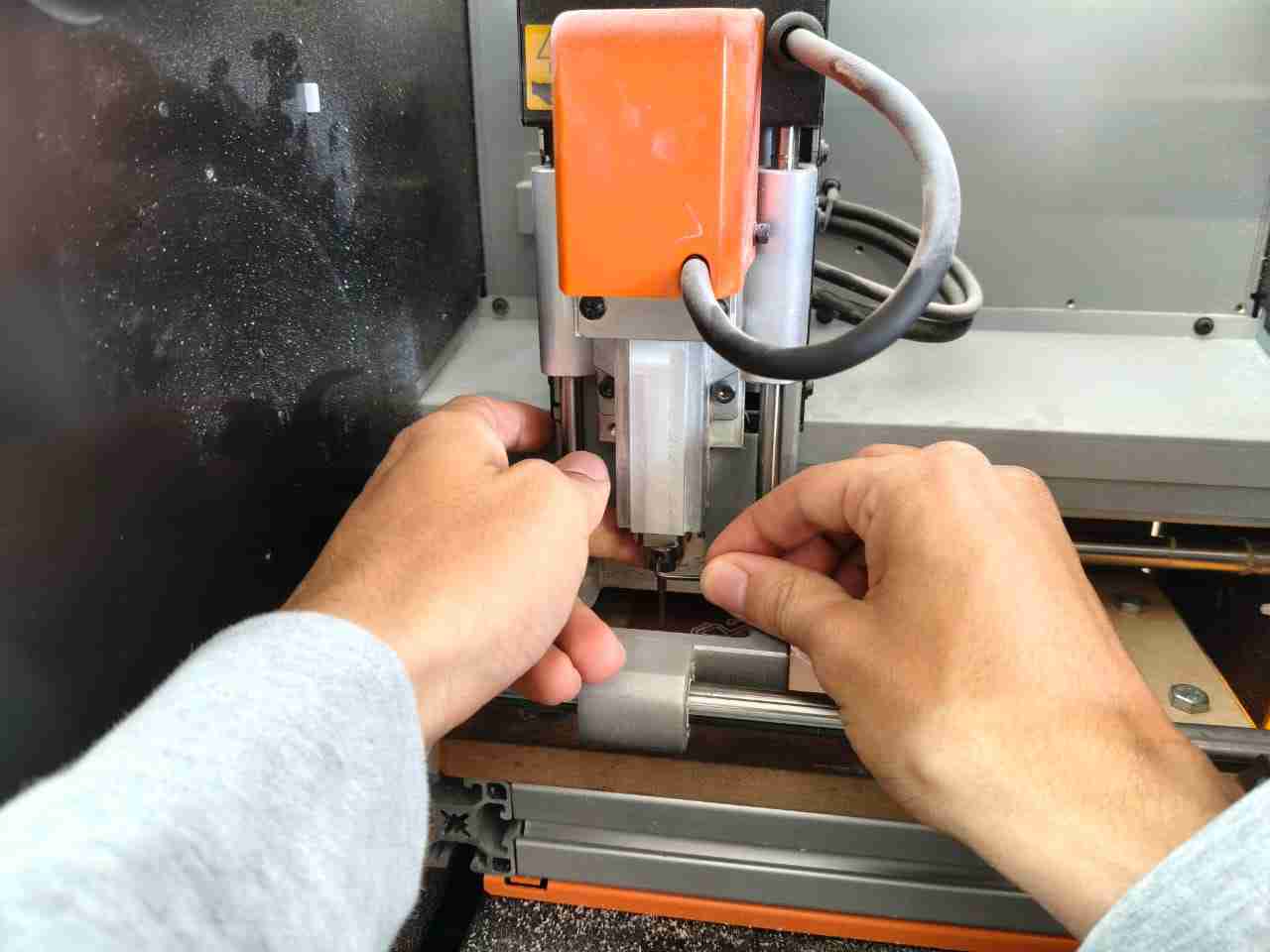
Before beginning the milling process, we must first position the spindle directly above the desired origin on the XY plane. Then, we use the set origin point controls to save that location. As a result, the values of the X and Y axes in the user coordinate system will reset to zero once the origin is saved. It is important to note that the monoFab machine features sensors that detect when the front panel is open; if this condition is present, the V-panel will prompt a message instructing the user to close the panel to resume operation.
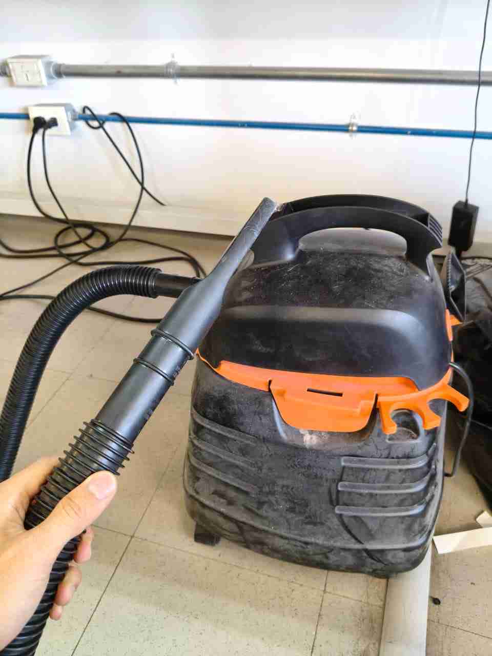
Even though the monoFab machine is enclosed, we must clean it with a vacuum cleaner to prevent inhaling residual dust. Milling tools can be changed with Allen keys.
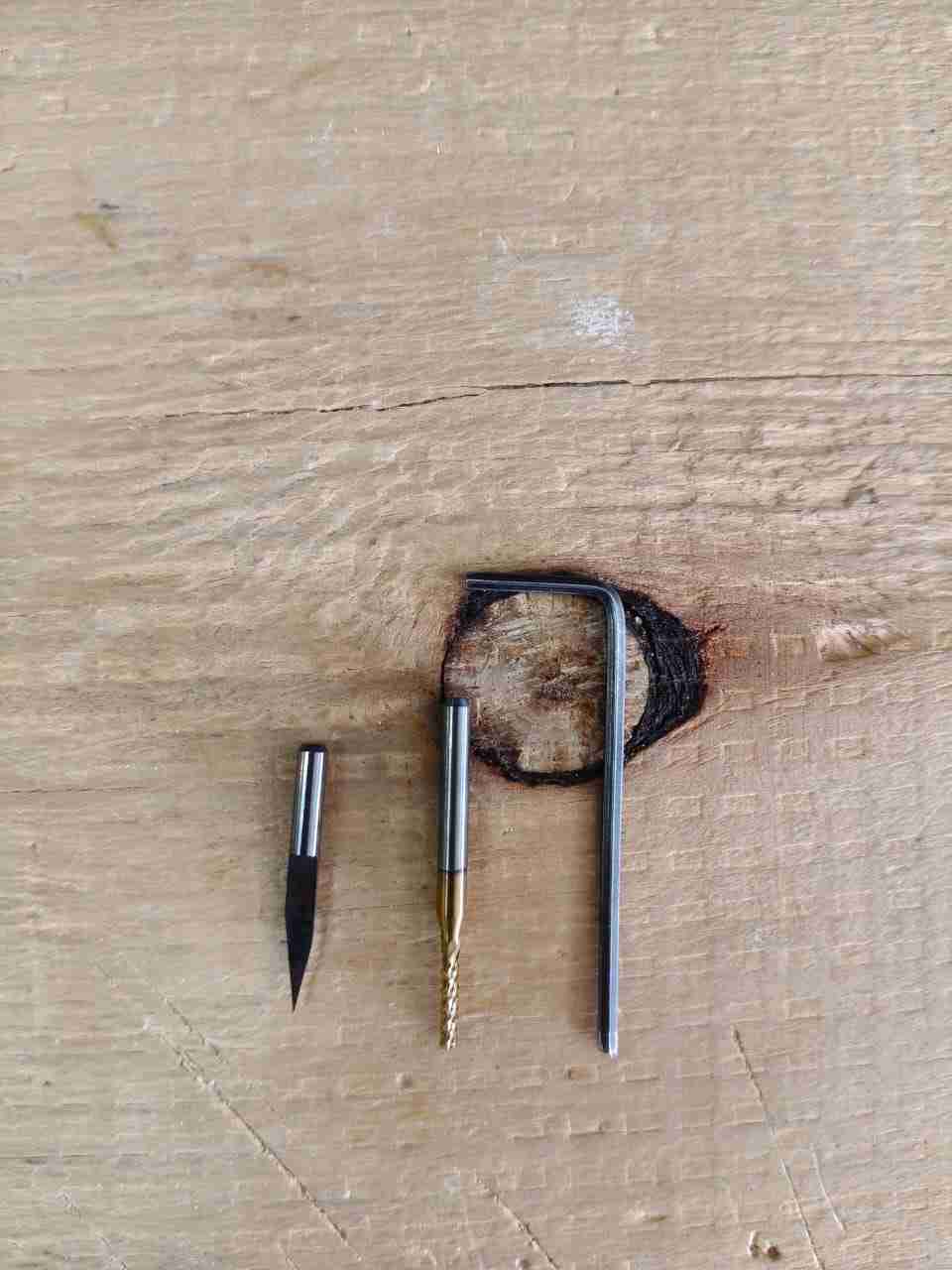
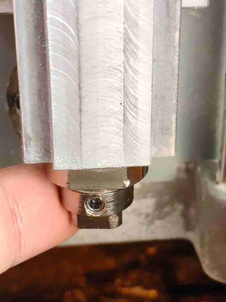
It is very important to make sure that the milling tool is tightly attached to the spindle so that it doesn't fall off while the machine is working. The V-tool is the first tool that needs to be used because this PCB doesn't have any through-hole parts. While setting the Z-origin, one way to make sure the V-tool is touching the phenolic board is to move the spindle with the tool attached and then loosen it. This will let the V-tool fall safely until it hits the phenolic board. This method might not guarantee that the PCB is level, but it is a good way to start the milling process.
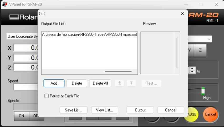
Once the origin is set along the three axes, we can proceed to load the desired .rml file using the "Set" button. This will open a menu that allows users to browse through .rml files, which are compatible with the Roland SRM-20 monoFab machine.
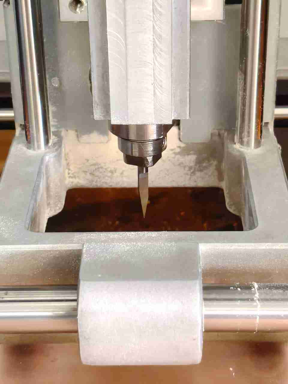
MonoFab machine during milling operation.
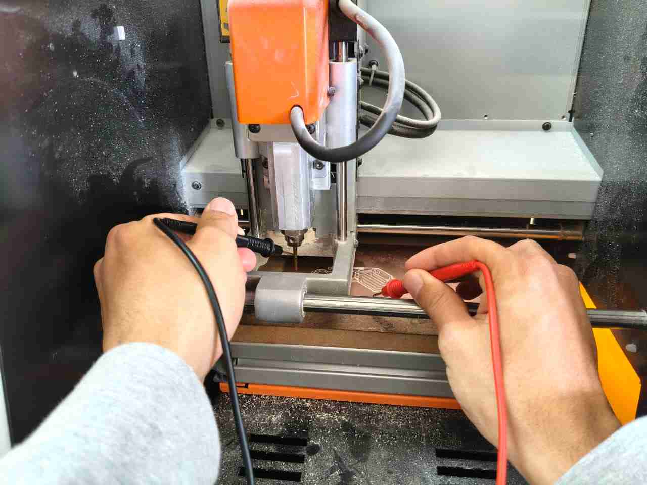
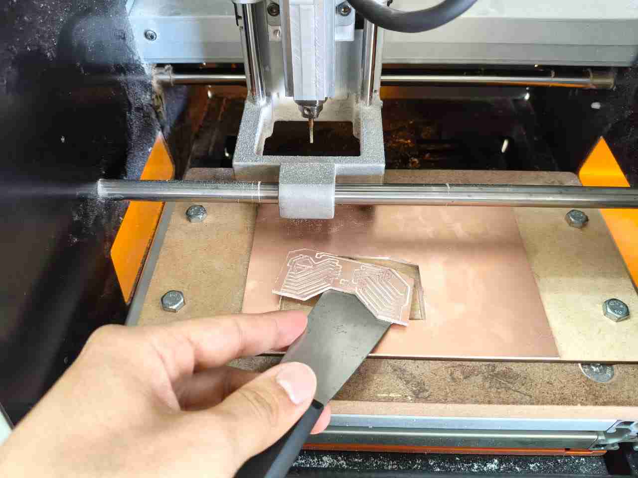
Since the lines have already been milled, we can now switch to the 2mm cutting tool. We need to keep the XY origin because we want to use the same one for the outline as we did for the traces. This time, I chose to use a multimeter to zero the Z-axis. The multimeter will make its unique buzzing sound if the tool head touches the phenolic board while it is in continuity mode. The buzzer may go off without proper contact with the object, which is known as a false positive, but at least this method gives you a sound to refer to.
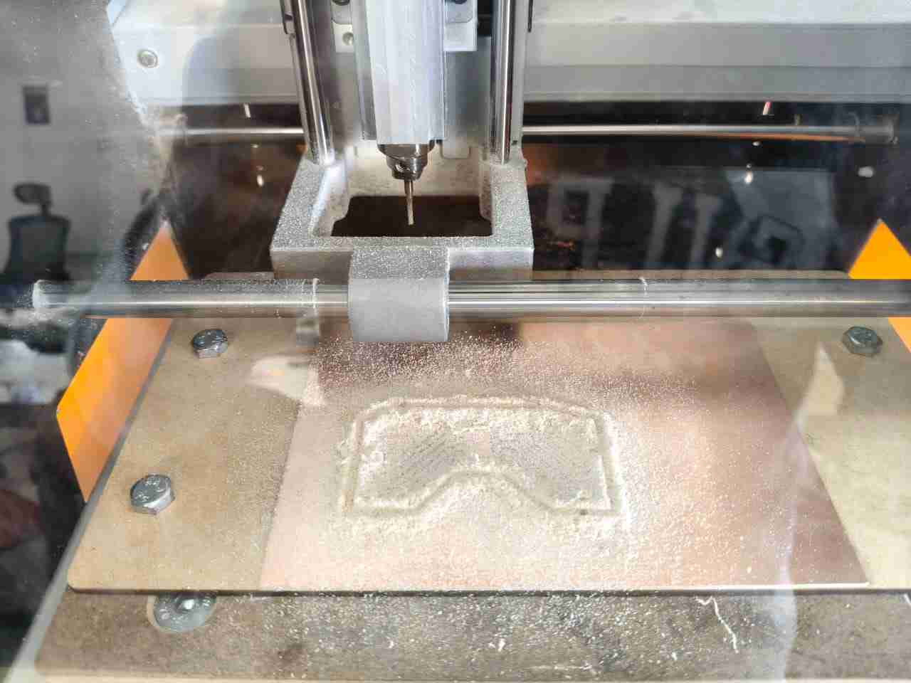
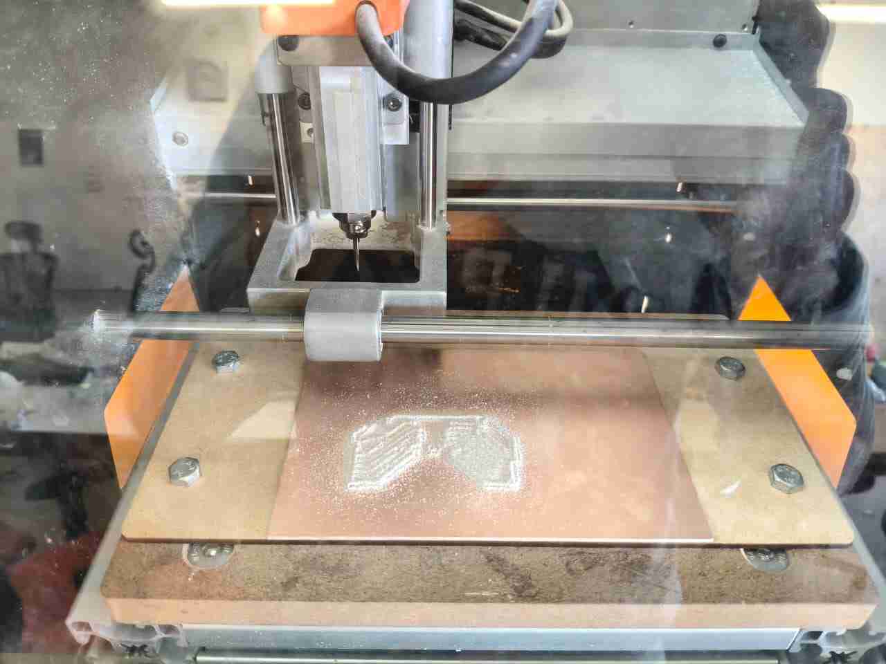
Remember, you should vacuum inside the monoFab between each milling operation to better visualize the quality of the in-process PCB.
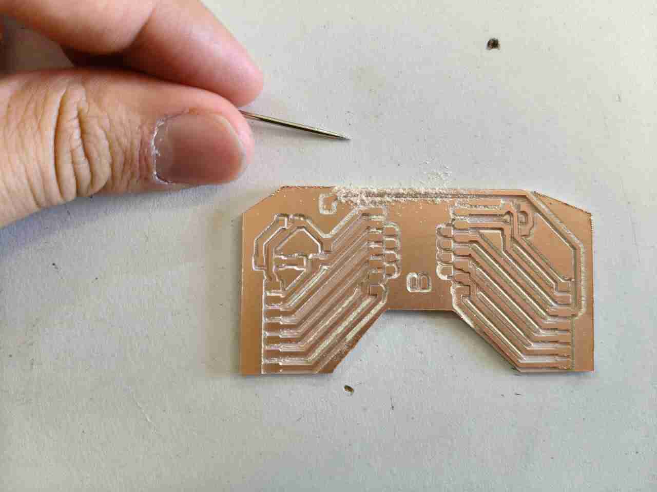
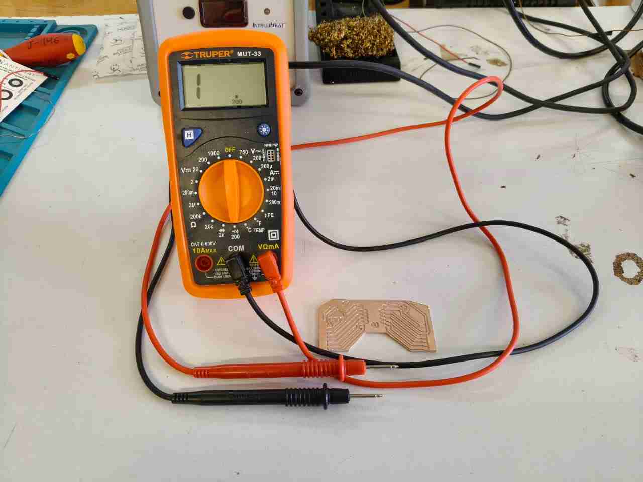
Post-processing operations for the PCB may involve removing dust with a needle and checking for continuity between isolated traces with a multimeter.
4. Soldering
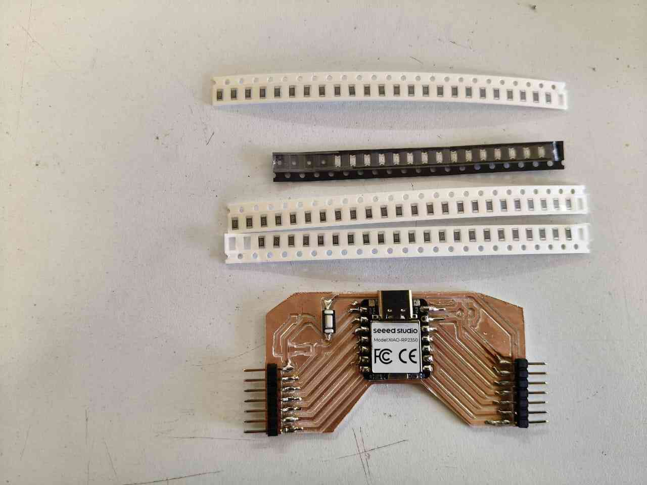
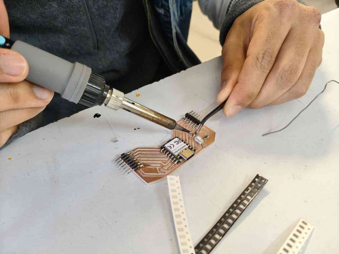
The soldering process can be quite challenging, particularly for those of us with unsteady hands, like mine. For individuals who struggle with this task, using tweezers or holders from a soldering station can greatly simplify the process. I usually set my soldering iron to 310 degrees Celsius, which is an optimal temperature for quickly melting solder without risking damage to components or melting pin headers. I started soldering my PCB using just my soldering iron and a pair of tweezers, although I also had solder suckers on hand. It is essential to regularly dip the soldering iron tip in flux to ensure proper adhesion of the solder and effective heat transfer.
To solder SMD components, we can start by placing the tip of the soldering iron on top of a pad. Next, we should bring some solder into contact with the same area where the tip of the soldering iron touches. Since heat tends to move toward colder regions, the solder will flow toward the copper pad, completing our first solder joint. The Xiao RP2350 is the main component of the PCB, so we need to attach it to one solder pad first. Thereafter, we must solder the opposite pad to ensure the board is aligned correctly.
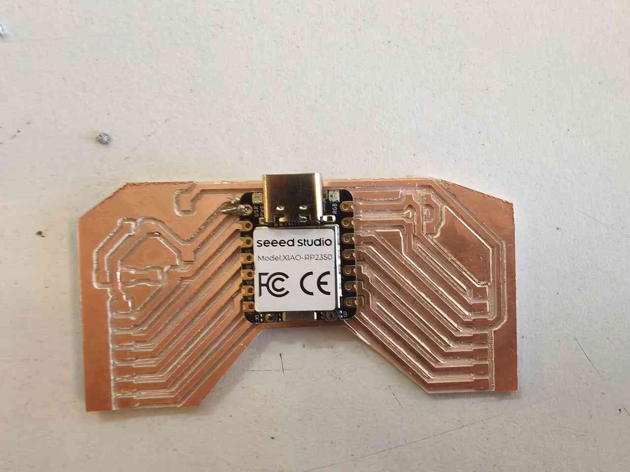
Once I soldered the opposite pads, I moved on to solder the remaining pads. After the Xiao board was fully soldered, I then soldered the pin headers using my tweezers.
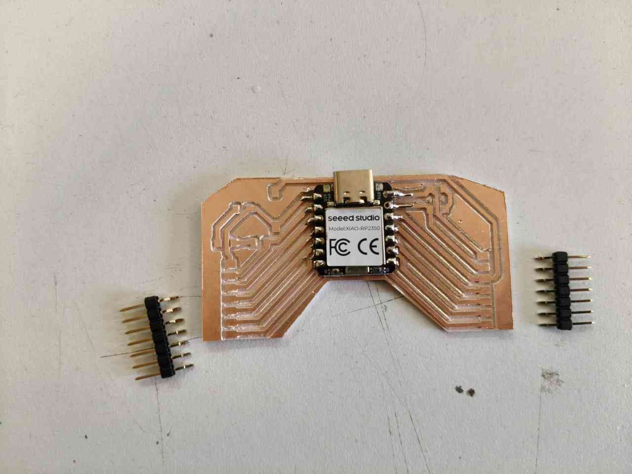
With the Xiao board and the pin headers in place, I proceeded to add the button, resistors, and LEDs.
After the PCB was fully soldered and validated using a multimeter, I proceeded to upload an Arduino code that would help me test if the Xiao board could be flashed and the peripherals properly used. The code would set the Xiao board to wait for the press of a button to toggle its peripheral LED between the on and off states. The following code was written with the assistance of ChatGPT using the following prompt: Write a code for a Xiao RP2350 board that constantly reads the state of a pull-up button in order to toggle an LED.
                const int buttonPin = D1;      // Push button Pin
                const int ledPin = LED_BUILTIN; // LED peripheral
                bool ledState = false;
                bool lastButtonState = HIGH;

                void setup() {
                pinMode(buttonPin, INPUT_PULLUP);
                pinMode(ledPin, OUTPUT);

                // LED turned off at start
                digitalWrite(ledPin, HIGH);
                }

                void loop() {
                bool buttonState = digitalRead(buttonPin);

                // Botton interaction detection
                if (lastButtonState == HIGH && buttonState == LOW) {
                    ledState = !ledState;

                    if (ledState) {
                    digitalWrite(ledPin, LOW);   //  LED ON
                    } else {
                    digitalWrite(ledPin, HIGH);  // LED OFF
                    }

                    delay(200); // Simple antidebounce
                }

                lastButtonState = buttonState;
                }
5. Through-Hole PCB
Producing a PCB with through-hole components requires the additional step of machining holes first. The file generation follows a workflow similar to the one previously described.
For drill generation, we could follow a workflow similar to that used for the outline, but we will need to employ a different control for selecting the tool. Since through-hole components typically use 1.24 mm pins, it is beneficial to drill with a 0.8 mm tool.
6. Files
Here are the downloadable files for this week:
KiCad schematic and Code for the Xiao RP2350 microcontroller boardReflection
At the end of this assignment, I can say that I can reliably produce PCBs with the tools available at the FabLab. I was confused at first by some nuances from mods CE, but it did not take long for me to get a handle on these new tools. I am looking forward to continuing to use these tools.