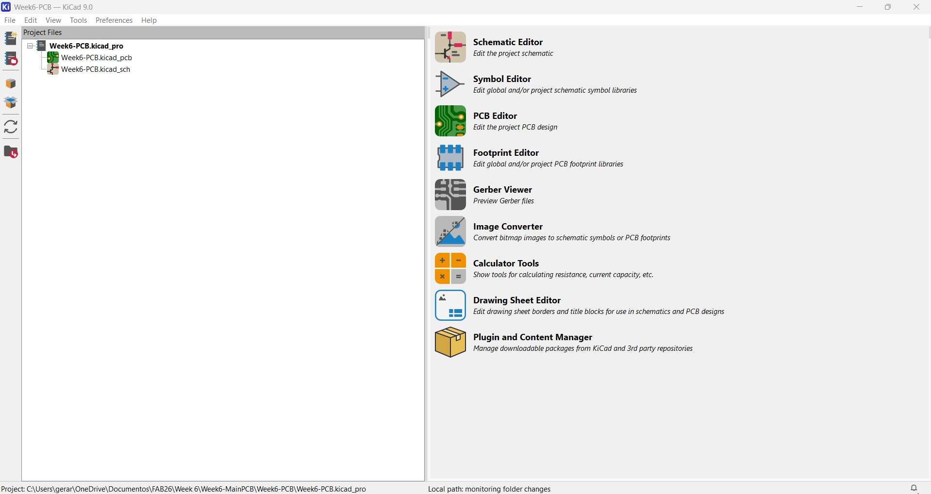
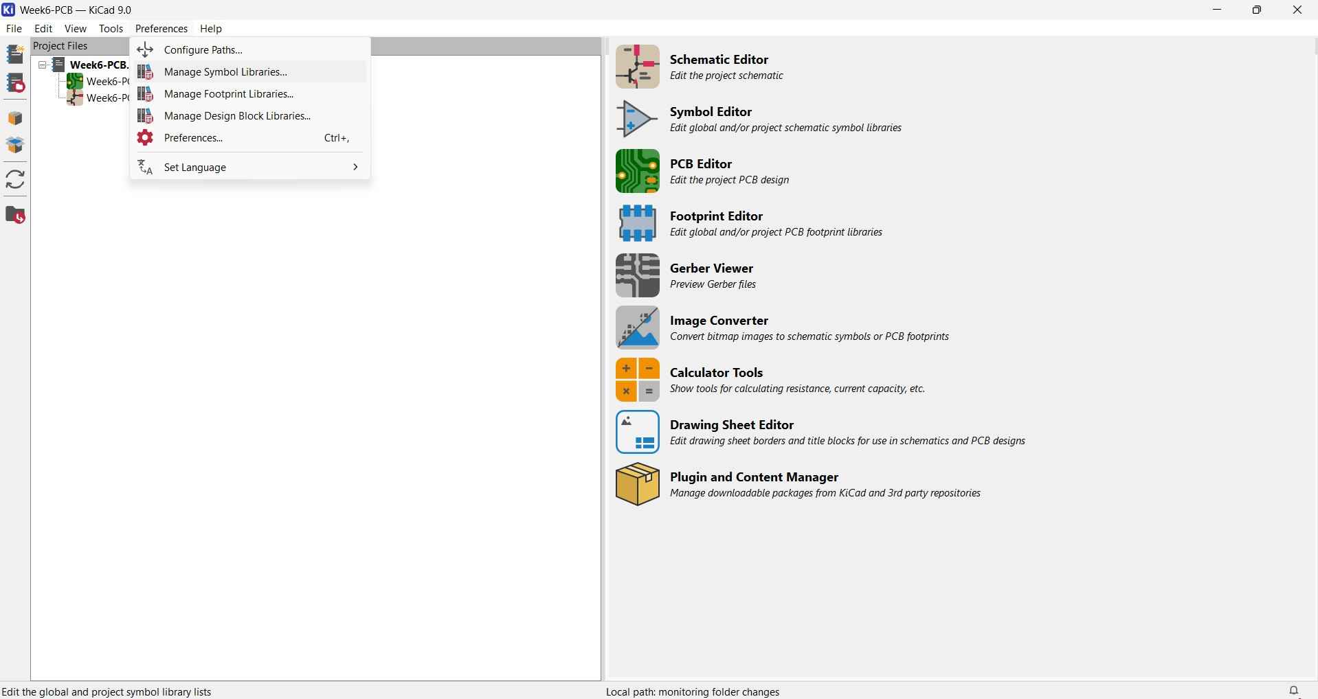
Week 06: Electronics Design
This week, we focused on electronics design, which involves transforming a functional idea into a manufacturable circuit. This process includes selecting electronic components, determining their connections, and ensuring compliance with design rules. For our assignment, we were tasked with designing and documenting the main printed circuit board (PCB) that will be used in upcoming assignments related to electronics. For this week's group assignment, the test equipment in our lab was used to observe the operation of a microcontroller circuit board. Click here to check on this week's group assignment page.
Work log
Completed tasks
- Evaluated EDA software
- Designed PCB layout
- Documented design decisions
1.What is a PCB?
A printed circuit board (PCB) serves as a physical base that supports and electrically connects the components of an electric circuit. Almost all modern consumer electronics, like phones, tablets, smartwatches, wireless chargers, and power supplies, use PCBs. A protoboard circuit and a PCB can implement the same schematic, but they differ in how the connections are made. In a protoboard, connections are made with jumpers, solder bridges, or point-to-point wiring, making them ideal for stages of experimentation when frequent changes are expected. In contrast, connections on PCBs are etched onto one or more layers according to a designed layout, which ensures reliability and efficiency.
A PCB is often made from a combination of strong, nonconductive materials that provide insulation, water resistance, and temperature stability. Common PCB materials include fire retardant 4 (FR4), metals, and polyimide (PI). When choosing materials for a PCB, it is important to consider factors such as cost savings, functional performance, eco-friendliness, and, perhaps most importantly, the tools available for manufacturing.Within a PCB, signals travel between points through thin etched pathways known as traces. These traces are typically composed of copper, a highly conductive material that enables electrons to move with minimal resistance between active and passive electronic components.
Active electronic components require electrical power to operate and perform functions such as switching, controlling, processing, or amplifying signals. Typical examples include transistors, operational amplifiers, and integrated circuits. In contrast, passive electronic components do not provide power gain or amplification; their main function is to store, dissipate, or transfer energy within the circuit. Common examples are resistors, capacitors, inductors, and transformers.
Early PCB designs relied on through-hole construction, which required electronic components to be inserted into holes on the circuit board. Through-hole components provide stronger mechanical attachment, are easier to prototype and hand-solder, and are often simpler to test and replace manually. However, these components take up more space and require drilled holes, which can increase PCB fabrication time and cost. Today, surface mount technology (SMT) has largely replaced through-hole components in PCB mass production. SMT components are significantly smaller, allow for higher component density, and have shorter leads that can reduce parasitic inductance and capacitance. However, SMT components can be more challenging to hand-solder and rework, and some packages are too small for easy manual probing.
2.EDA Software
For decades, circuits were drawn by hand, resulting in a slow and inflexible manufacturing process. However, with the introduction of computer-aided design (CAD), printed circuit boards (PCBs) could be designed similarly to mechanical components. This advancement accelerated production and allowed for easier error detection and updates. Electronic Design Automation (EDA) software suites provide tools for designing, simulating, verifying, and preparing PCBs for manufacturing.
The PCB design process encompasses:
- Schematic creation: Designers create a two-dimensional blueprint of the printed circuit board (PCB) using Electronic Design Automation (EDA) software, which allows them to identify components, their placement, and the connections between them.
- Material selection: Designers choose board materials based on the requirements of the final assembly, considering both performance needs and the malleability of the substrate. Substrates can be rigid, flexible, or a combination of both. Common material options include FR-4, polyimide laminates, composite epoxy materials (CEM), and liquid crystal polymer, among others.
- Design review:To proceed with production, simulation software is employed to test and validate the performance of the PCB under various conditions. These tests ensure that the design choices, such as the selection and placement of components as well as the length and shape of the traces, meet all specified requirements.
3.KiCad
I have worked on KiCad in the past, and I wish to deepen my knowledge of this tool. Additionally, the Fab Academy team shared with us a library with plenty of symbols and footprints for electronic components that we may use throughout the remainder of the course.
For starters, KiCad is an open-source software suite designed for creating electronic circuit schematics and printed circuit boards (PCBs). It features an integrated workflow that enables users to design a schematic in conjunction with its corresponding PCB. Additionally, KiCad offers various utilities to assist with circuit and PCB design. These include a PCB calculator for determining trace width, resistance, and current capacitance; a Gerber viewer for inspecting manufacturing files; and an integrated SPICE simulator to validate circuit behavior. KiCad is compatible with Windows, macOS, Linux, and Docker, and it supports PCBs with up to 32 copper layers, making it suitable for designs of varying complexities.
4. My PCB design
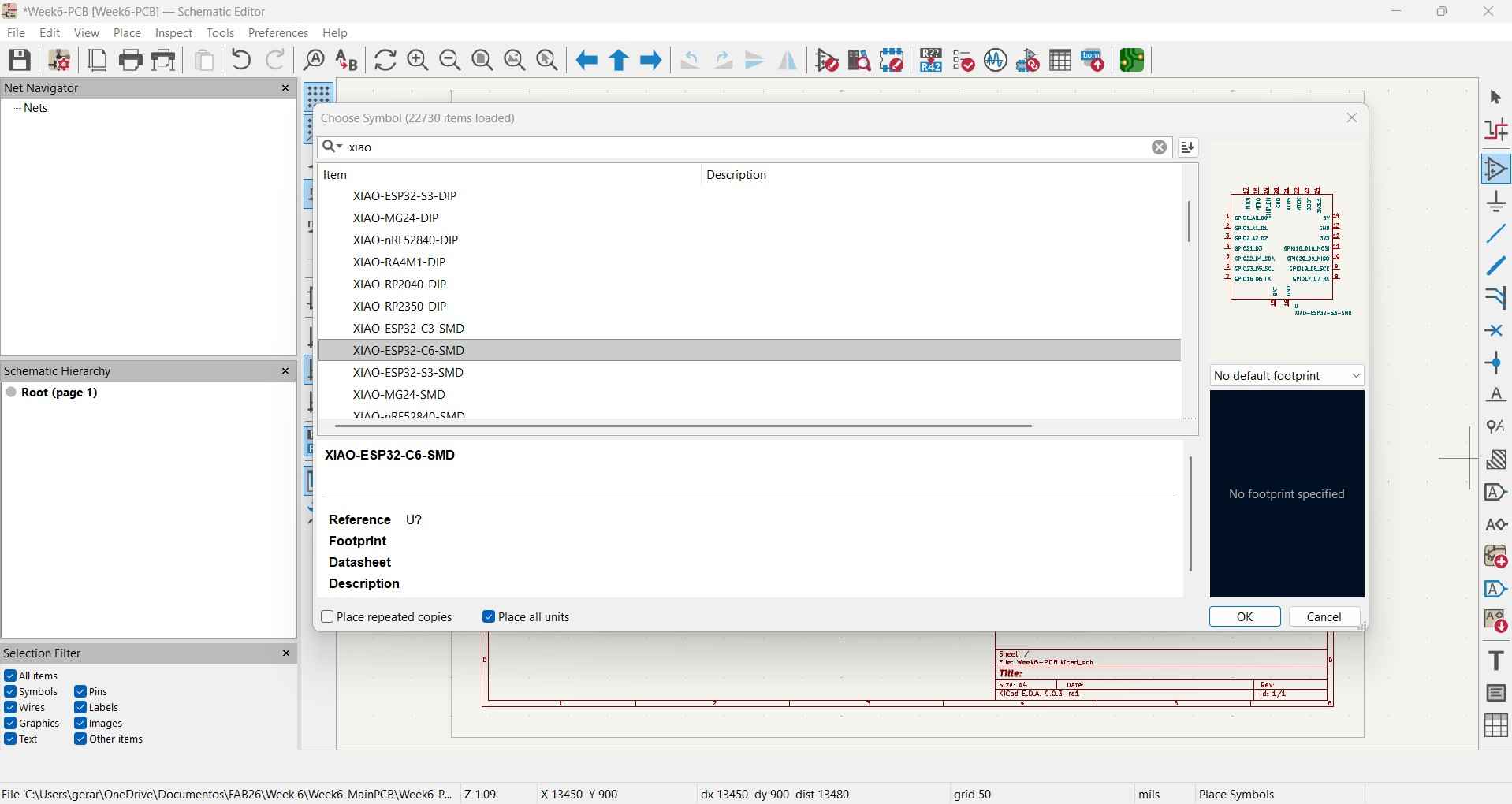
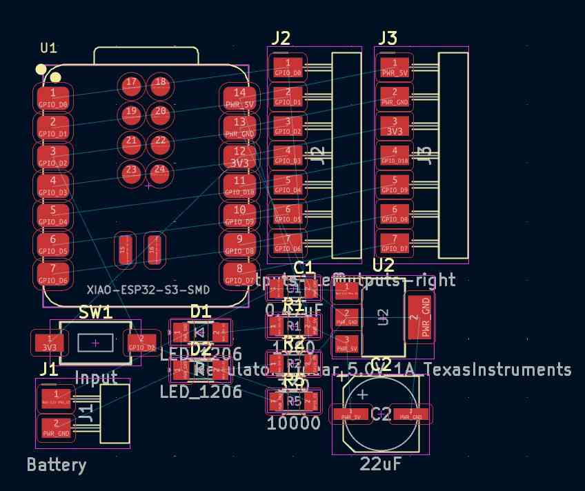
This week, I designed the PCB that I will use in my upcoming electronics assignments and to get acquainted with a microcontroller that I will use for my final project. The PCB I designed is based on the Xiao ESP32C6 board, as I aim to utilize its connectivity options and processing power to assist with debugging during indoor testing and to serve as the brain of my robot. Furthermore, the Xiao ESP32C6 can host RTK rover firmware and instructions for relaying commands to other microcontrollers. This capacity will be useful since an RTK module like the UM982 can interface with the Xiao ESP32C6, perform positioning operations, and relay that information to the Xiao without overloading it. Another design consideration I took into account when designing this board was the tools available for fabrication. FabLab Puebla is currently equipped with CNC3018 and monoFab SRM-20 milling machines, which are ideal for manufacturing one-layer PCBs. However, manufacturing double-sided PCBs with these machines can be a daunting challenge; as such, I decided to make my design a one-layer PCB. Another design consideration was the surface-mount package size; our local instructor advised us to use 1206 SMT components. That number is based on the component's dimensions in inches: 12 = 0.12 inches long and 06 = 0.06 inches wide, which is approximately 3.2 mm x 1.6 mm; those dimensions are still comfortable for manual soldering.
4.1. Getting started with KiCad
After downloading and installing KiCad, you will see its main interface when you open the software. The first step should always be to save your project, just as you would in any other software. In KiCad, you can do it by navigating to the File menu located in the upper bar of the interface and selecting "New Project", or by clicking on the top icon in the left sidebar.
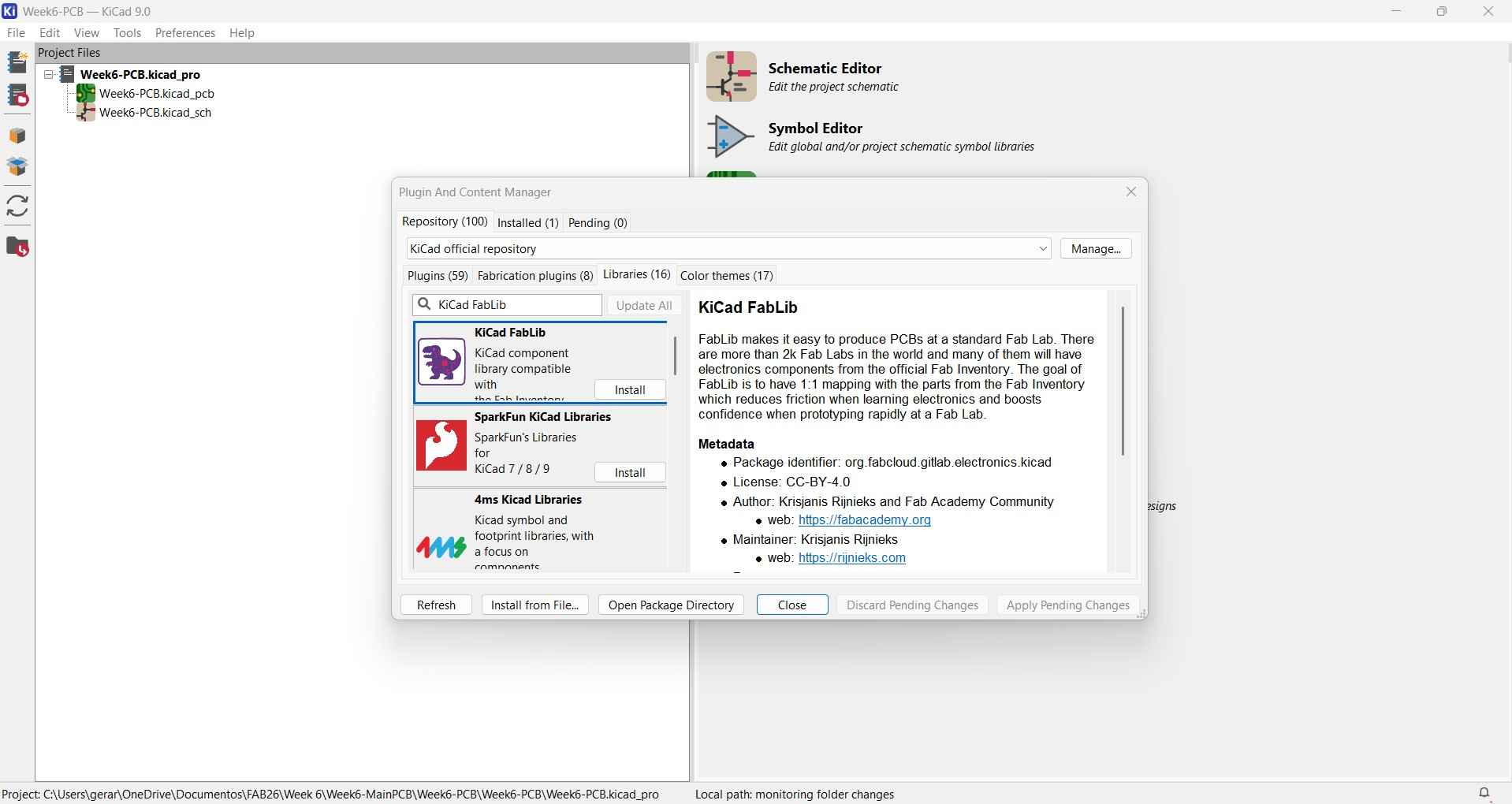
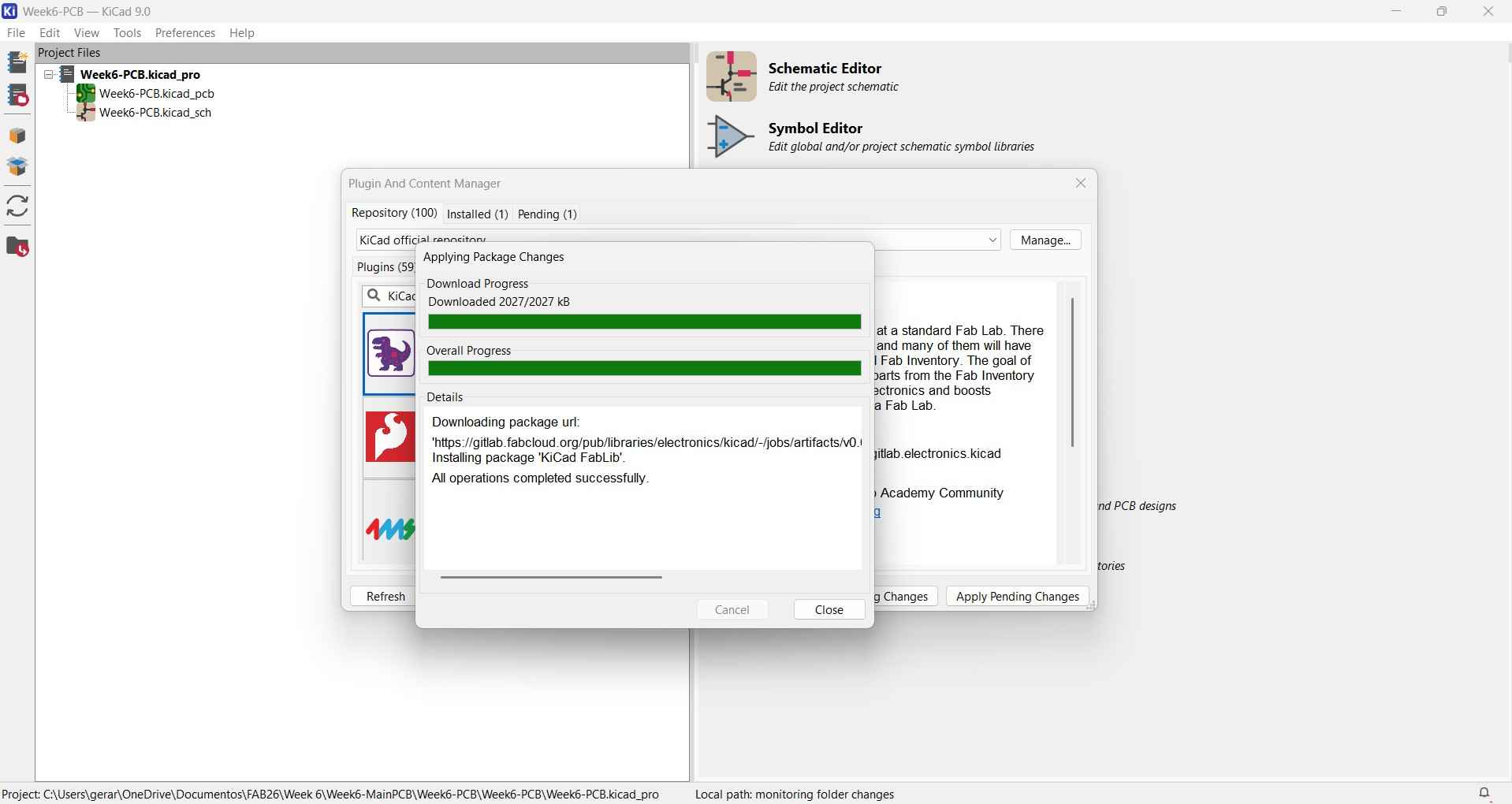
Before I began designing my PCB, I first installed the component library provided by the Fab Academy team to ensure compliance with the necessary component packages and sizes. There are two methods to install a library. The first method involves clicking on the icon for the "Plugin and Content Management" menu, which opens the plugin and content management interface. This interface features a search bar for locating specific add-ons organized into four categories: Plugins, Fabrication Plugins, Libraries, and Color Themes. To find the Fab Academy Library, I entered "KiCad FabLib" into the search bar. I chose to download the top option on the list because its description included links to the repository maintained and updated by its users. After clicking "Install" and then "Apply pending changes," a window titled "Applying Package Changes" will pop up, showing two progress bars along with details such as the download URL and operation status. Once the progress bars are complete, we can click "Close."
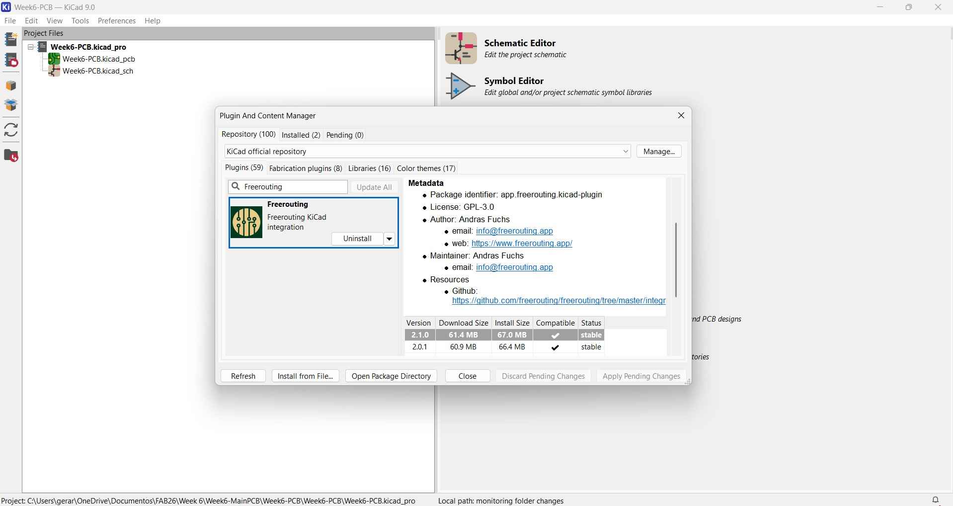
I also installed the Freerouting library, which adds an autorouter for the KiCad PCB editor. I recommend using this autorouter for repetitive but simple connections, as I found that with complex connections on a single-layer PCB, the tools offered by this library may be insufficient.
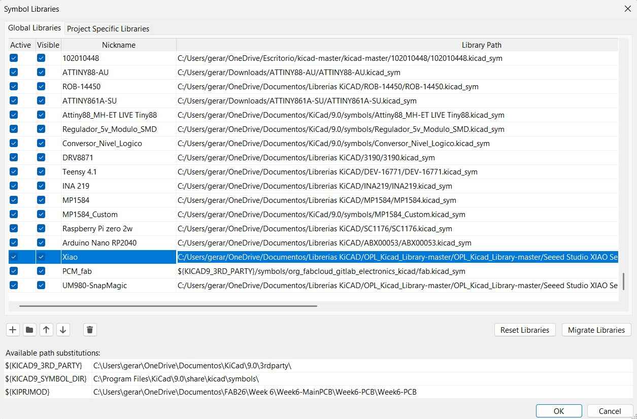
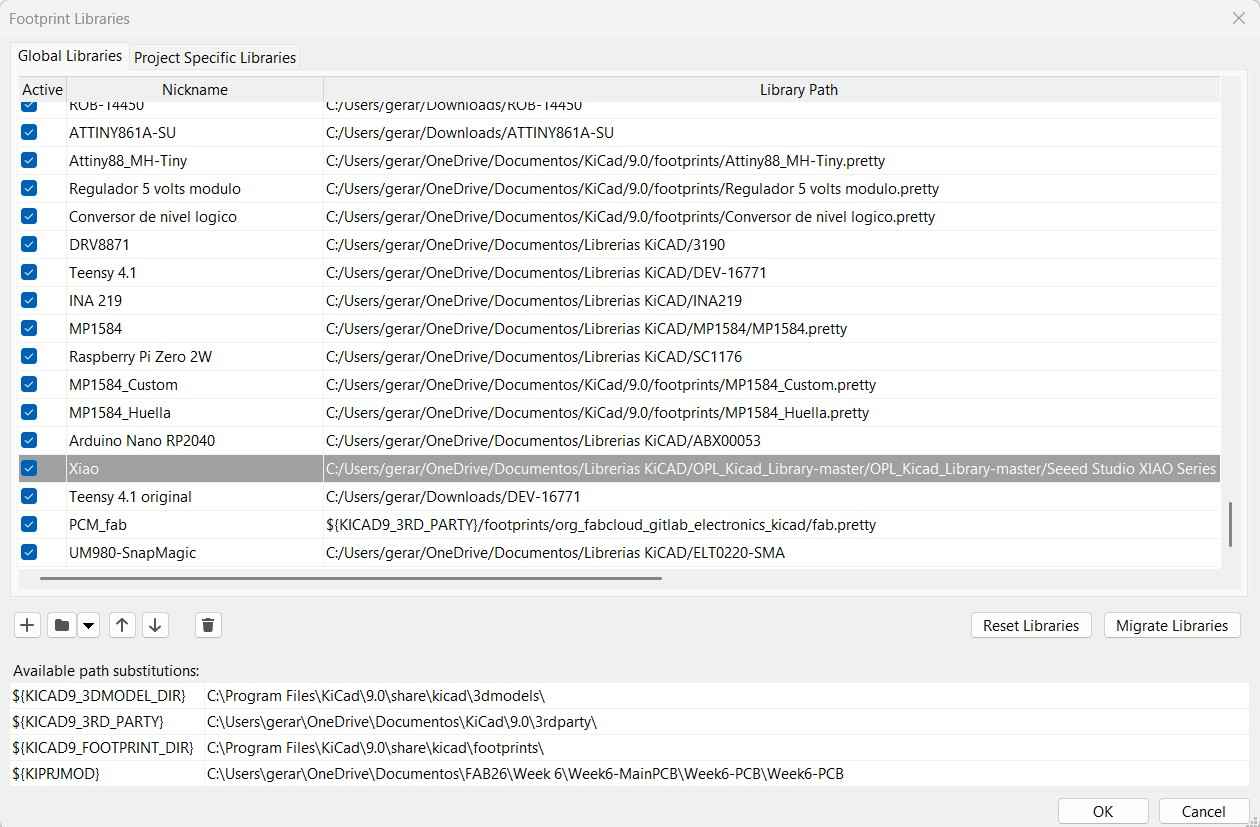
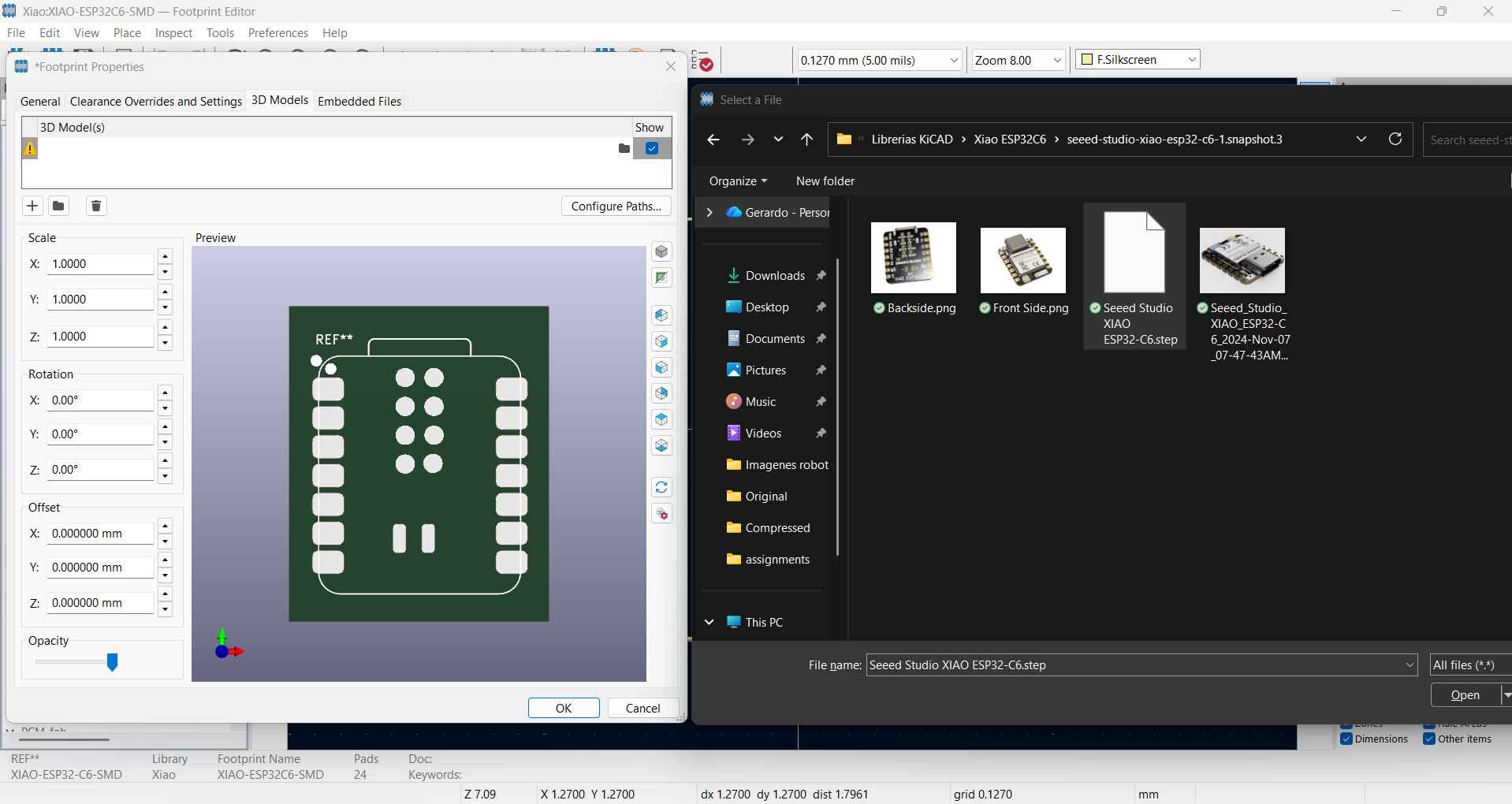
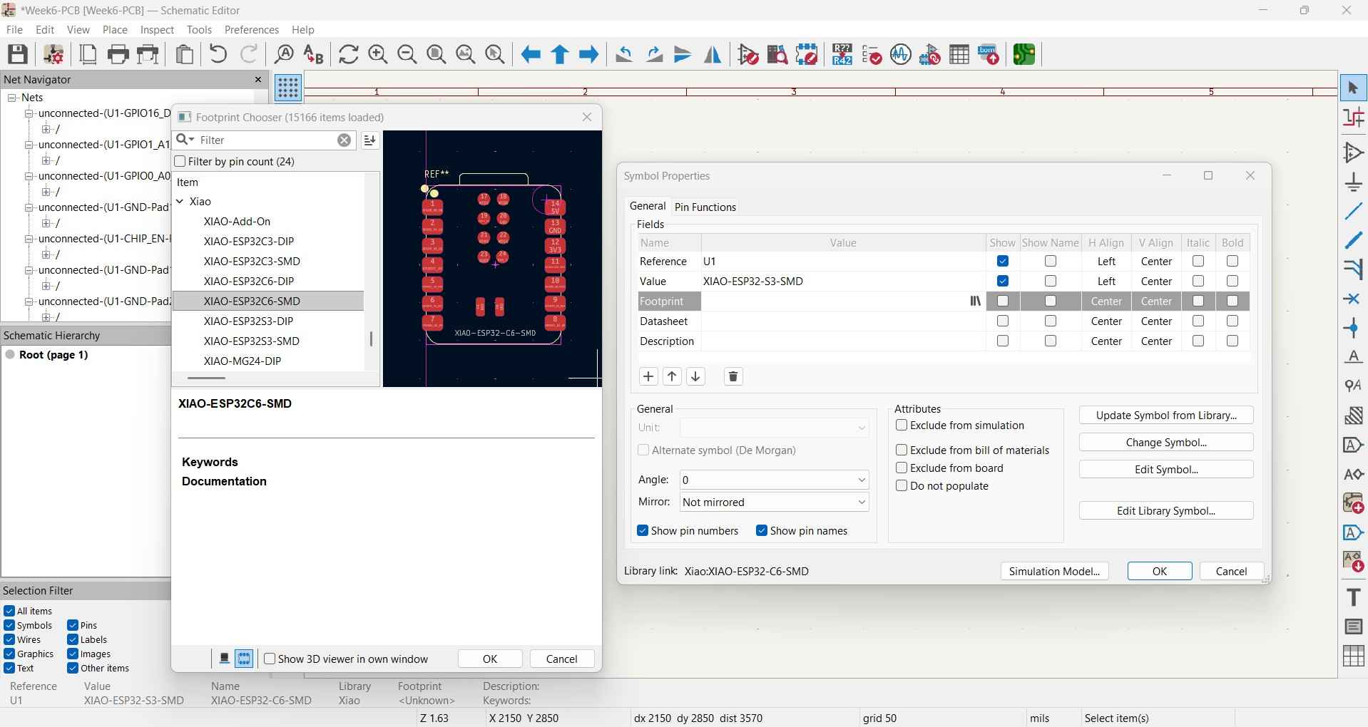
To illustrate the second method for installing libraries, I will use the "Preferences" menu located in the top bar of the main interface. Some electronic component footprints and schematic symbols may not be available in the "Plugin and Content Manager", prompting users to search for these items in alternative repositories. Fortunately, websites like SnapMagic and Seeed Studio regularly update their repositories, providing options to download files in formats compatible with KiCad. In my case, I was looking for the symbol, footprint, and 3D model for the Xiao ESP32C6 board. The Fab Academy library contains the symbols and footprints for several Xiao boards that could act as placeholders. However, the Seed Studio website had the symbol and footprint I was looking for, and for the 3D model, the site provided a link to a GrabCAD account that contained the necessary files for the model I was looking for. To add these elements to my KiCad environment, I used the second method, which involves using the Preferences menu on the KiCad main interface.
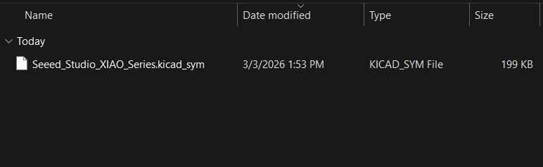
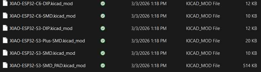
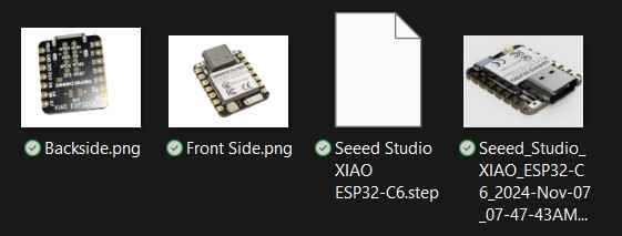
Once the folders containing each type of file are decompressed, if the download proceeds without any problems, our folders should include one file with the .kicad_sym extension. This file contains all the symbols from the boards currently offered by Seeed Studio. A second folder should contain several files with the .kicad_mod extension, which correspond to the footprint files for each board currently available from Seeed Studio. A third folder should contain the .step file, which represents the 3D model.
File with the .kicad_sym extension:
Files with the .kicad_mod extension:
File with the .step extension:
To add a new symbol to our libraries, we have to choose the Manage Symbol Libraries option under the "Preferences" menu.
After selecting the previously mentioned option, the Symbol Libraries menu will appear. A bar with five icons, beginning with a "+" symbol, will be displayed at the bottom of the menu. Clicking this icon will create a new row for the library. In the first column, enter the name of the library that will house the new symbol. In the second column, add the file path to the .kicad_symbol file by clicking the folder icon that appears when you hover your mouse over that column. After selecting the file and clicking the "Open" button in your browser, the file path will be added, and you will only need to click the "Ok" button in the Symbol Libraries menu.
Adding an electronic component's footprint is almost the same as adding a symbol. The major difference is that the process starts by selecting the "Manage Footprint Libraries" option under the Preferences menu. Additionally, the .kicad_mod file may not be visible when trying to add its path while viewing it through our file browser opened from KiCad. In this case, the program will focus on localizing the folder containing the file rather than the file itself.
To link a .step model to a footprint in KiCad, follow these steps:
- Open the Footprint Editor: Click on the Footprint Editor icon located on KiCad's main interface.
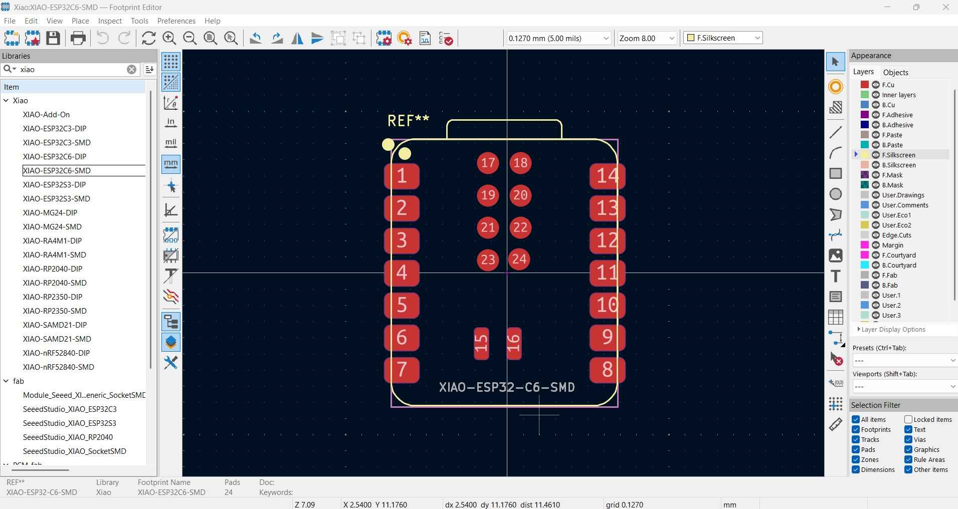
- Search for the Footprint: Once the Footprint Editor window appears, use the search bar to type the name of the footprint you need. This will display the footprint for your chosen component.
- Open Footprint Properties: Double-click the desired footprint to bring up the properties window.
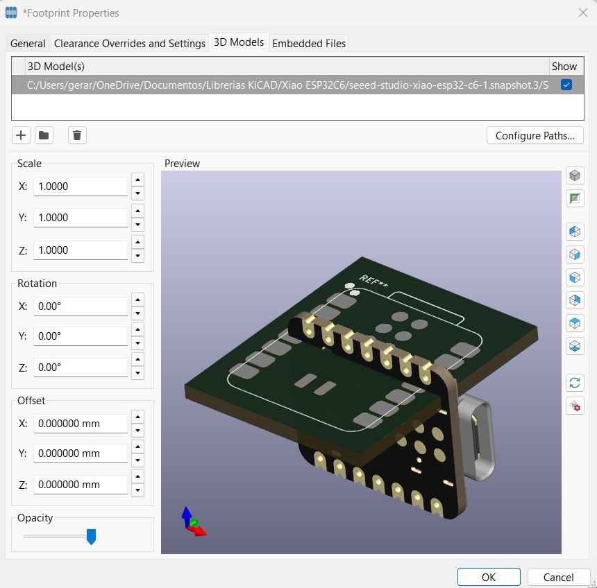
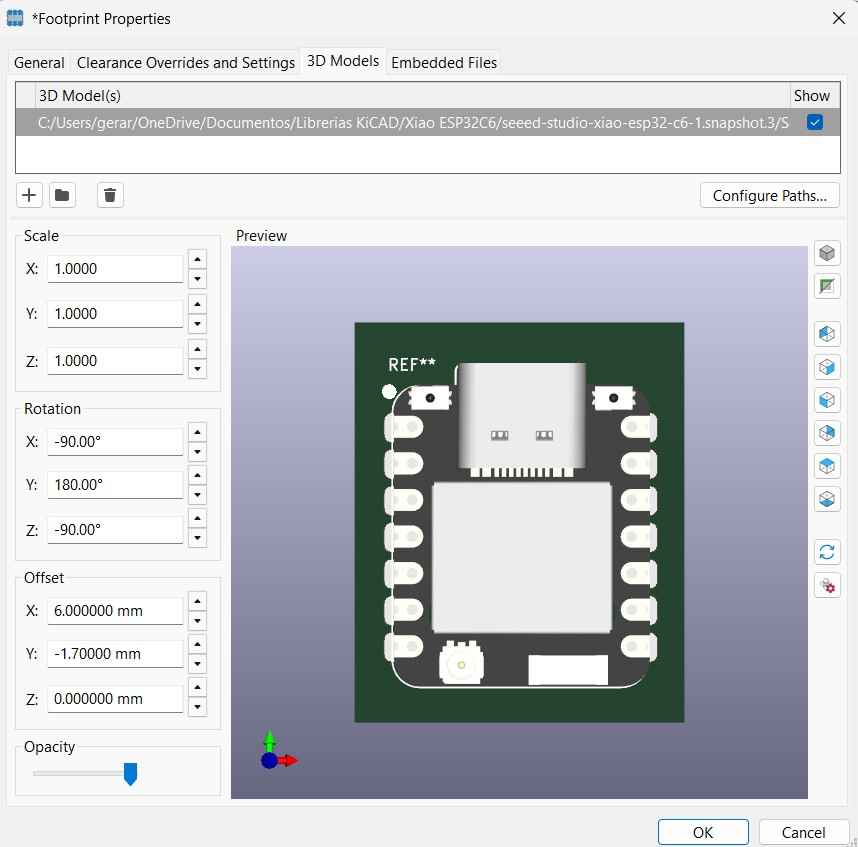
- Add the STEP Model: In the properties window, navigate to the "3D model" section. Here, you can add a .STEP model from your files.
- Adjust Placement: KiCad will attempt to automatically align the 3D model with the PCB holes. If needed, you can fine-tune the model’s position and orientation using the Scale, Rotation, and Offset controls. With everything set and done, click Ok to save the changes.
4.2. Schematic Design
A PCB design begins in the Schematic Editor, where we place the components for our circuits and establish the connections between them. A circuit must always include voltage and ground terminals, as current needs a complete path and a defined reference point. Current can be interpreted as a stream of electrons that flow through a pathway or trace; these electrons are pushed by a source, called voltage, through the circuit. These electrons need a return path and a common reference level that lets every part of the circuit "agree" on what 0V is. If there is no supply path, components receive no usable power; if there is no return path, current cannot flow in a closed loop; and if there is no common reference, signals become ambiguous, unstable, or meaningless.
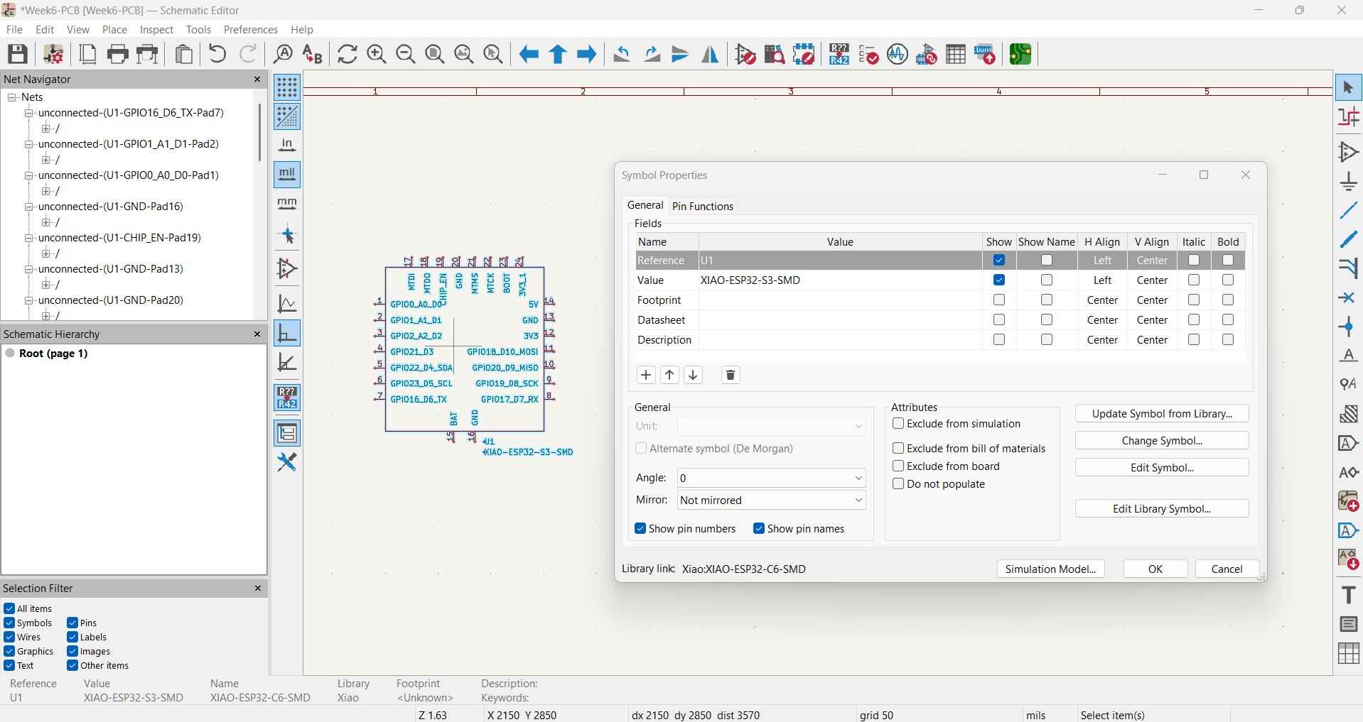
To place a component, click on the third icon from the top of the bar located to the right of the schematic editor. This will open the Choose Symbol menu. You can search for items in this menu by entering their names in the search bar at the top. Components are organized by libraries, and when you select a component, the menu will show its symbol and associated footprint. If a footprint is not linked to a component, you have the option to manually link it after placement. Once a component is selected, it will be highlighted in blue and can be moved within the workspace; left-clicking will place the symbol. Double-clicking on a symbol will bring up the Symbol Properties menu, where you can change the component reference, hide its label, add a description, and most importantly, link a footprint to the symbol.
Clicking the "Start print" button will prompt the slicer interface to show the "Device Window," which shows a panel for real-time monitoring and control. When using a K1C, this panel also shows video footage from the camera housed within the printer.
Clicking the footprint cell will open the Footprint Chooser. Footprints are also sorted by libraries and can be filtered using the search bar on top.
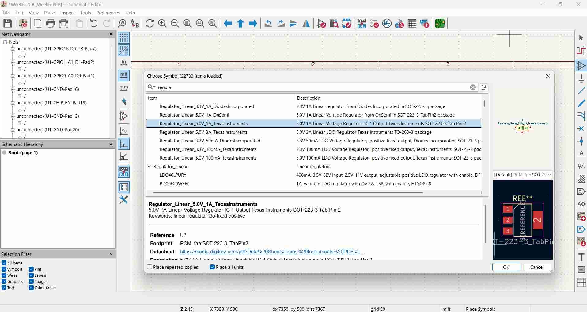
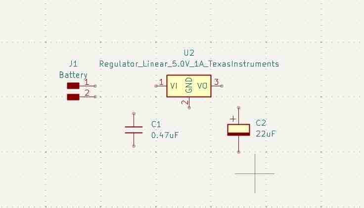
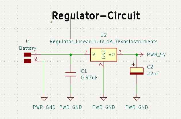
After placing the Xiao ESP32C6 board, I began designing the power supply section of the breakout board. I started by adding a couple of SMD horizontal pin header connectors to accommodate the voltage and ground terminals of a power supply. I also included a voltage regulator to adjust the input voltage to a level that would safely power the Xiao board, along with a couple of capacitors. My intention was to power the Xiao with a 5-volt signal. I selected a regulator from the fab library and included the capacitors according to the recommendations outlined in the regulator's library. It is advised to place a 0.47 µF capacitor between the unregulated voltage and the regulator's input pin, as well as a second capacitor at the output of the regulator, with a minimum value of 22 µF to maintain stability. The suggested values indicate that the input capacitor should be ceramic (without polarity), while the output capacitor should be electrolytic (polarized). A small input capacitor is usually placed to handle fast, high-frequency noise and spikes coming from the supply line, acting like a nearby fast reservoir. A larger capacitor is usually placed at the output of a regulator to handle larger changes in load current while keeping the regulator's output stable.
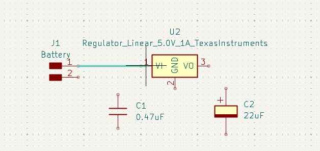
One method for connecting components in KiCad involves clicking on a terminal of one component and dragging the cursor until it reaches the terminal of another component. Once you have identified the terminal you wish to connect, simply click on the other terminal to finalize the connection.
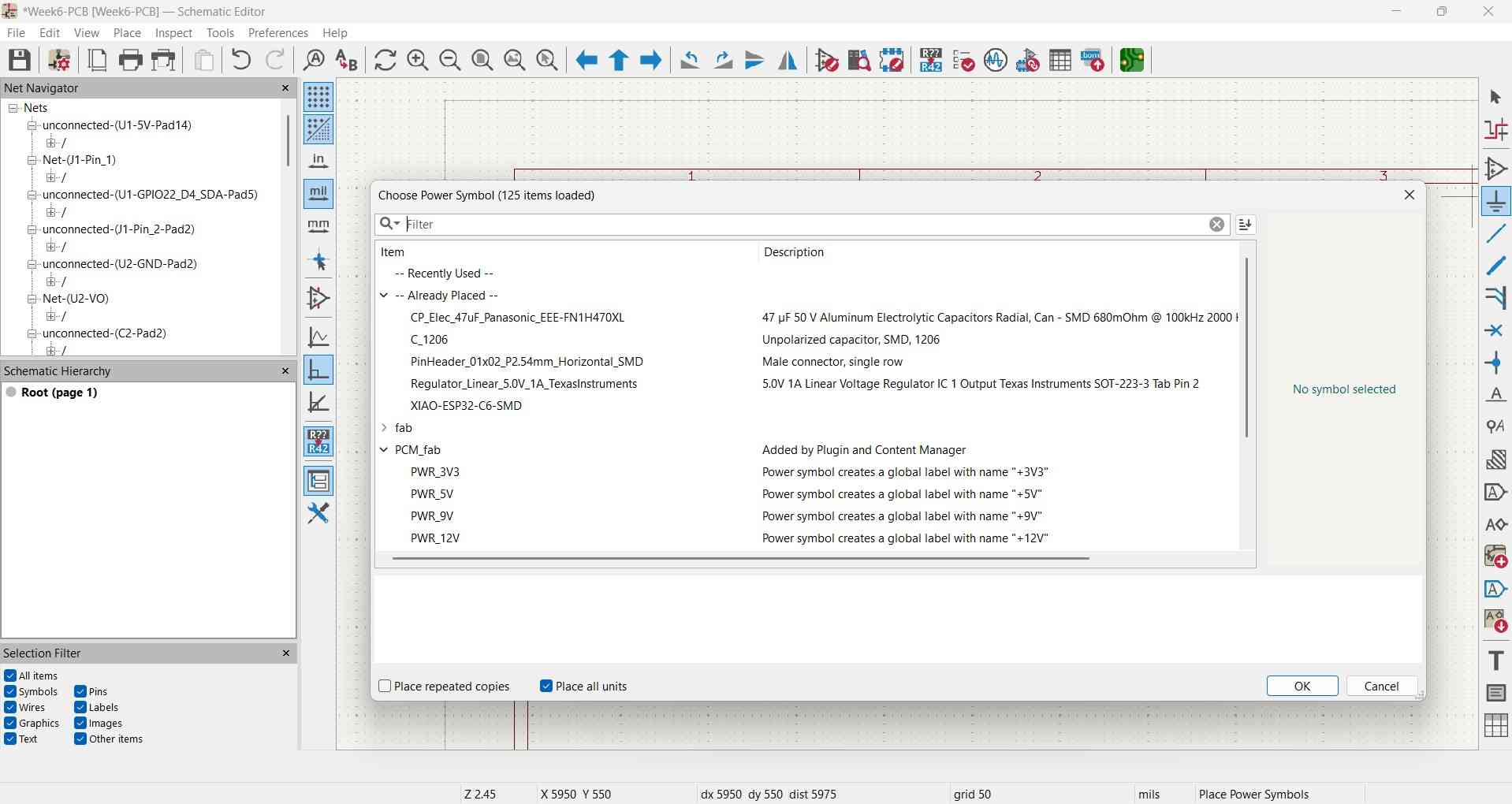
Symbols that represent a power output and ground terminal can be added by accessing the Choose Power symbol menu, which can be opened by clicking on the fourth icon of the bar on the right side of the interface.
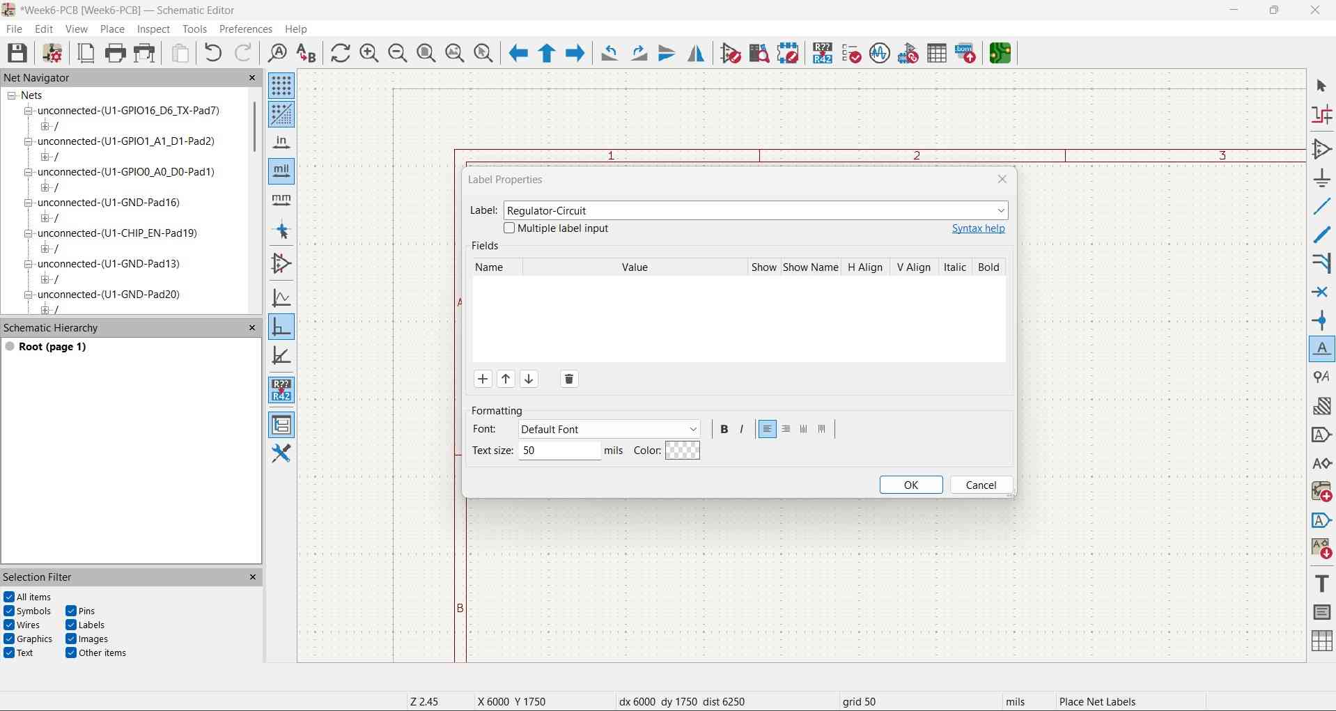
Labels can also be added to distinguish components or sections of a circuit.
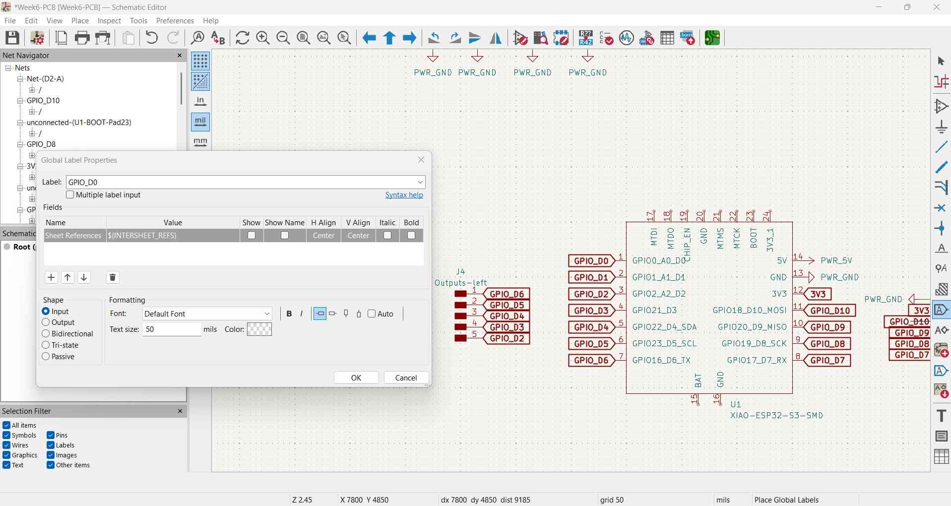
Another way to connect components in KiCad is by using global labels. These labels can be created and accessed by clicking on the thirteenth icon in the bar on the right side of the interface. To ensure they function correctly, one component should have a label designated as an input, while the other component should use the same label as an output.
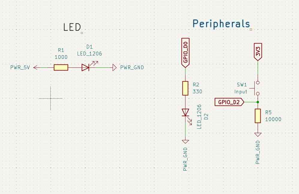
The circuit design features an LED connected in parallel to the Xiao board, functioning as an indicator. When the board is powered on, the LED illuminates, indicating that the board is energized. To prevent excessive current draw, I placed a 1000-ohm resistor in series with the LED. This resistor takes in the extra voltage and keeps the current at a safer level. Since my regulator provides 5V and a typical red LED requires 2V, the voltage across the resistor is calculated as 5V - 2V = 3V. Using Ohm's law, I can determine the current: I = V/R; thus, I = 3V/1000 ohms = 0.003 A, which is equivalent to 3 mA. The resulting current value still results in an LED with notable brightness.
I also included an additional LED connected to a pin from the Xiao board and a pull-down button. I included these elements to help me figure out if the board gets damaged. In case I suspect the board is no longer working properly, I could program the LED to start blinking following some pattern; if the LED does not respond, that means the board may be damaged or needs a hard reset. A similar logic applies to the button; when pressed, it will send a high logic value to its corresponding pin. If the Xiao can get that read, it means the board is still functioning.
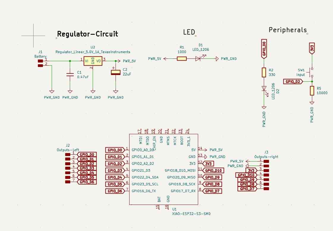
The schematic is complete. The pins on the Xiao board that can be soldered with through-hole pins have been connected to an SMT pin header, except for the two used for the LED indicator and the push button.
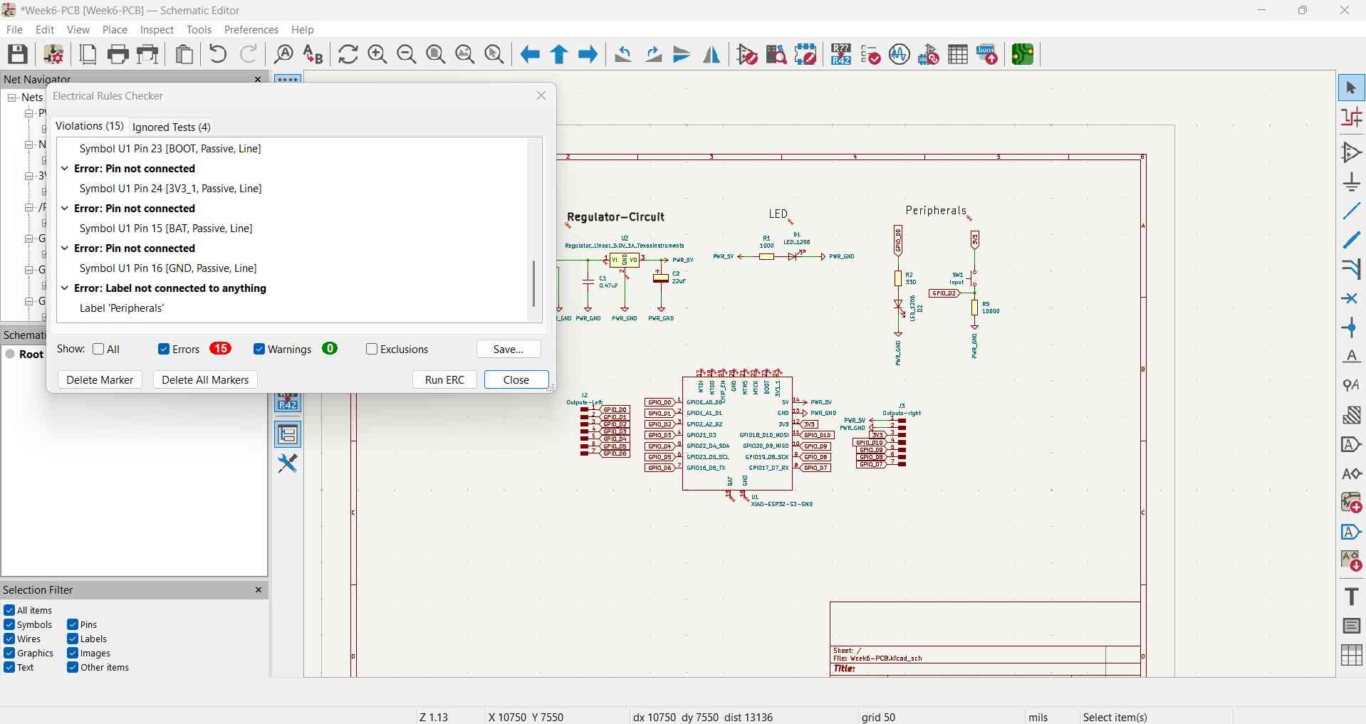
Before proceeding with the PCB design, I ran the Electronic Rule Checker (ERC) from the Inspection menu. This tool detects potential mistakes that could lead to circuit failure. However, it is important to understand what the ERC considers a mistake. For instance, in my circuit, I did not connect anything to the pins on the back of the Xiao board because I do not need them for the deliverables I am preparing for the upcoming assignments. Nevertheless, the ERC flagged these unconnected pins as potential issues.
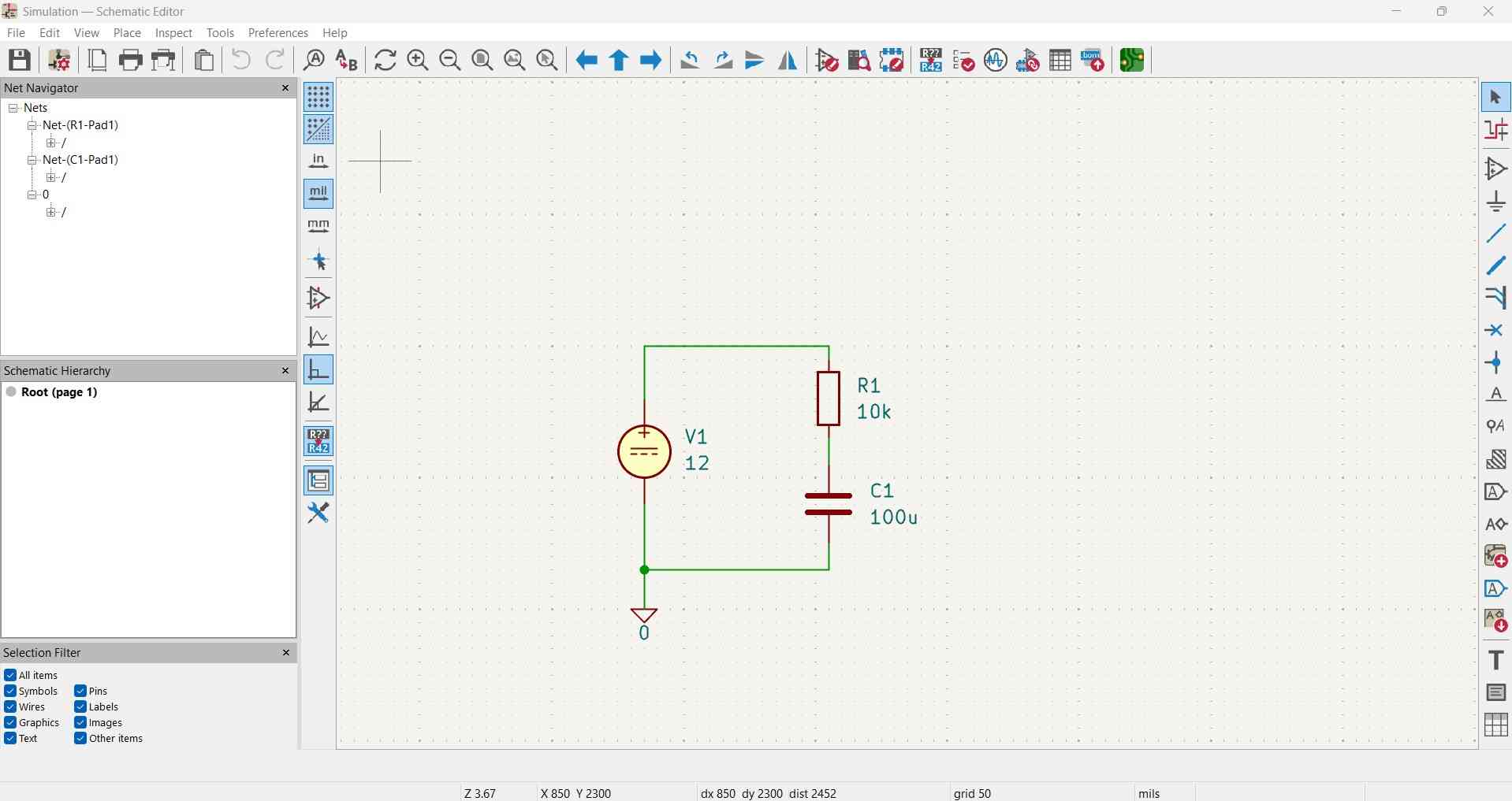
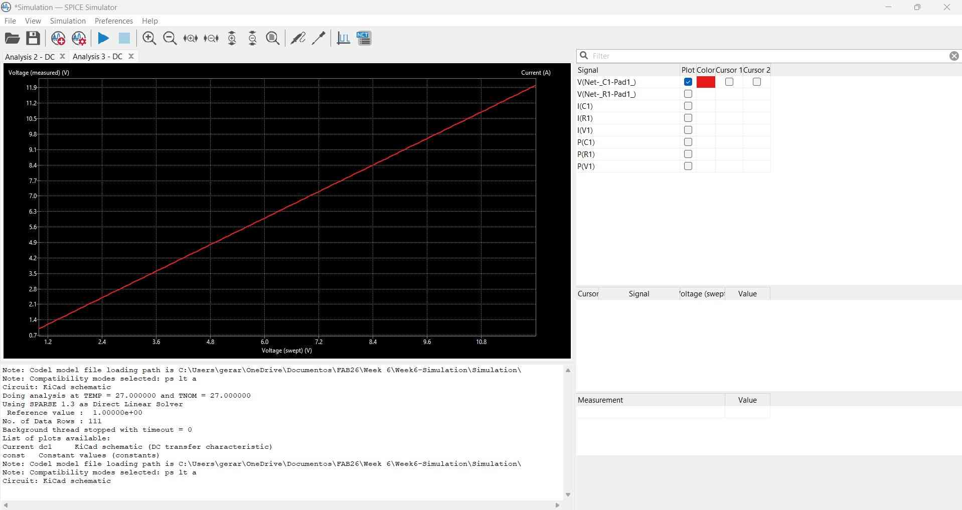
I would like to evaluate KiCad's simulation capabilities prior to reviewing my PCB design. KiCad can simulate electronic components if their SPICE models, which are standardized descriptions of electronic circuits, are available. While KiCad may not be the first choice for simulation among some users, it is essential to acknowledge this functionality offered by the EDA software.
Simulations in KiCad are performed using the schematic editor. To start, you need to place SPICE-compatible components and set their values by double-clicking on each symbol to edit their properties. In this simulation, I connected a resistor in series with a capacitor, along with a DC power supply.
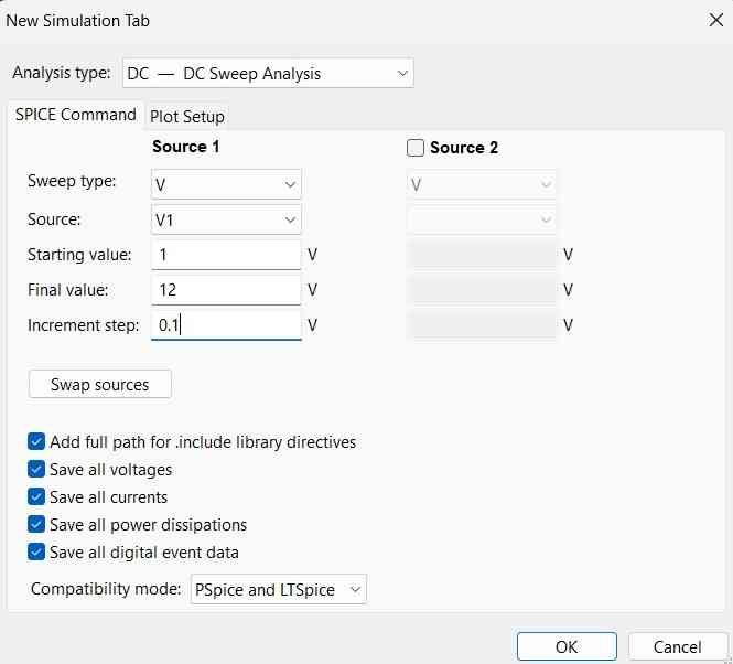
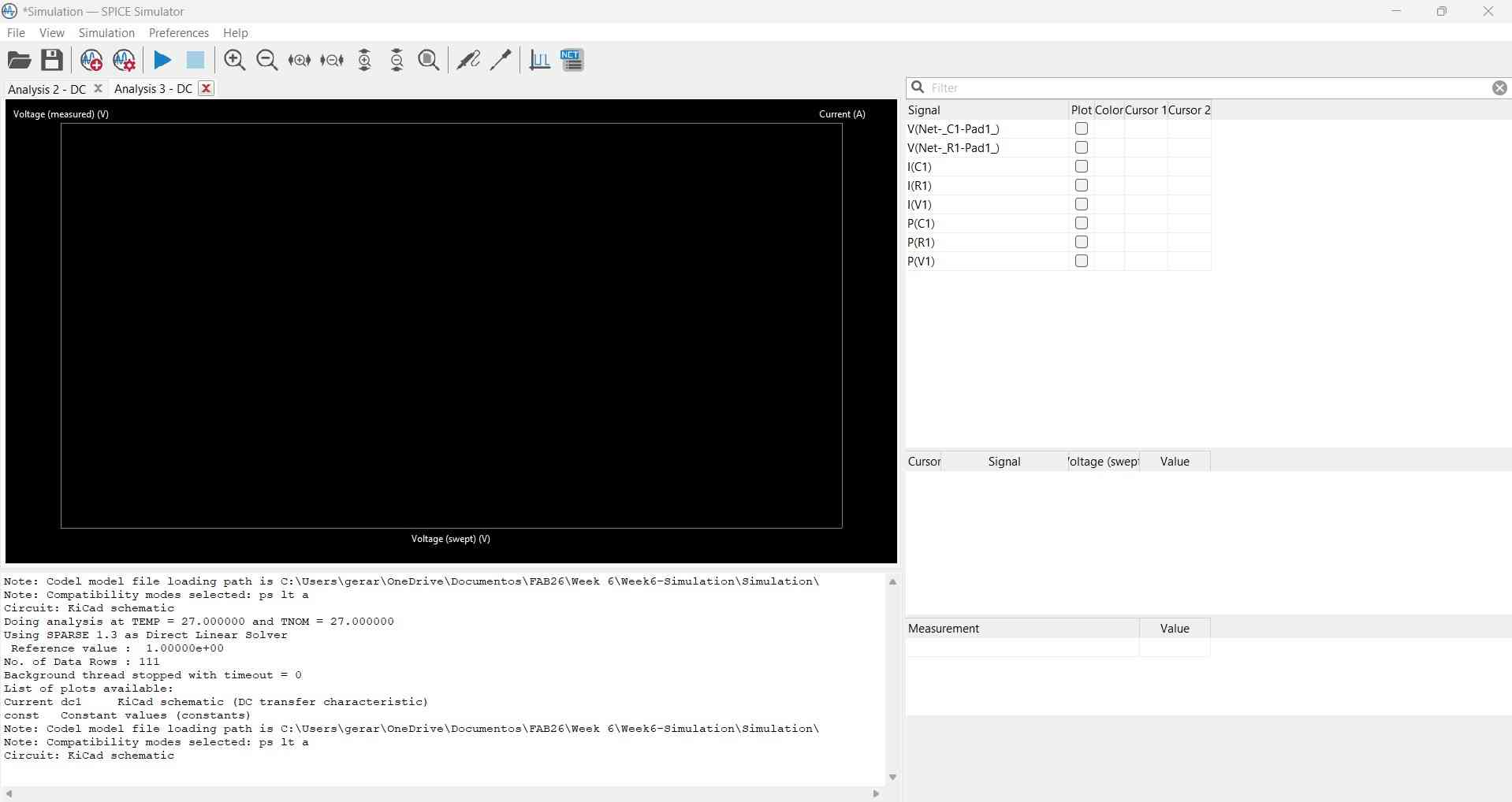
To initiate the simulator, click on the fifth icon from the right in the top bar. This will open the simulation tab, where you can select the type of analysis you wish to conduct. In this section, you will also need to specify the source, starting value, final value, and increment step. After completing these fields and clicking "OK," the simulator will present a screen that allows you to visualize various graphs related to the simulation. To view specific data, the final step is to place a probe on the circuit at the point where you want to measure a value. Once the probe is placed, the window will display a graph representing the requested data. In this instance, I requested information on the voltage stored by the capacitor and its relationship with the current.
4.3 PCB Design
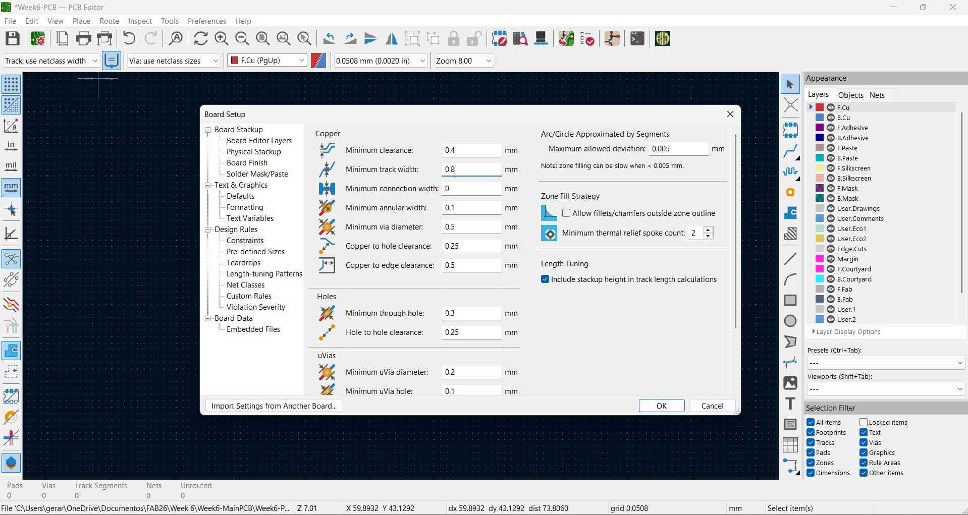
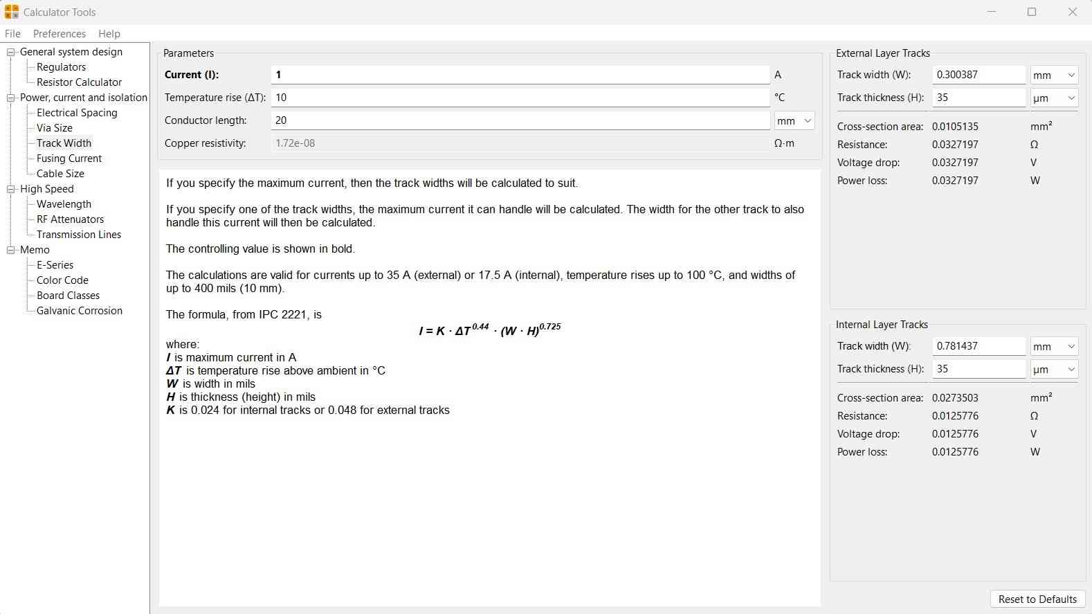
To translate our schematic to a PCB, we can open the PCB editor either from the schematic editor or from KiCad's main interface. Before proceeding with my design, I opened the Board Setup menu by clicking the icon resembling a PCB with a gear. I only changed the values for minimum clearance between traces and the minimum track width. I chose a minimum track of 0.8 mm, as that is the diameter of the V-tools used for engraving PCBs at FabLab Ibero Puebla, and as such, the minimum clearance is equal to the tool's radius, 0.4 mm.
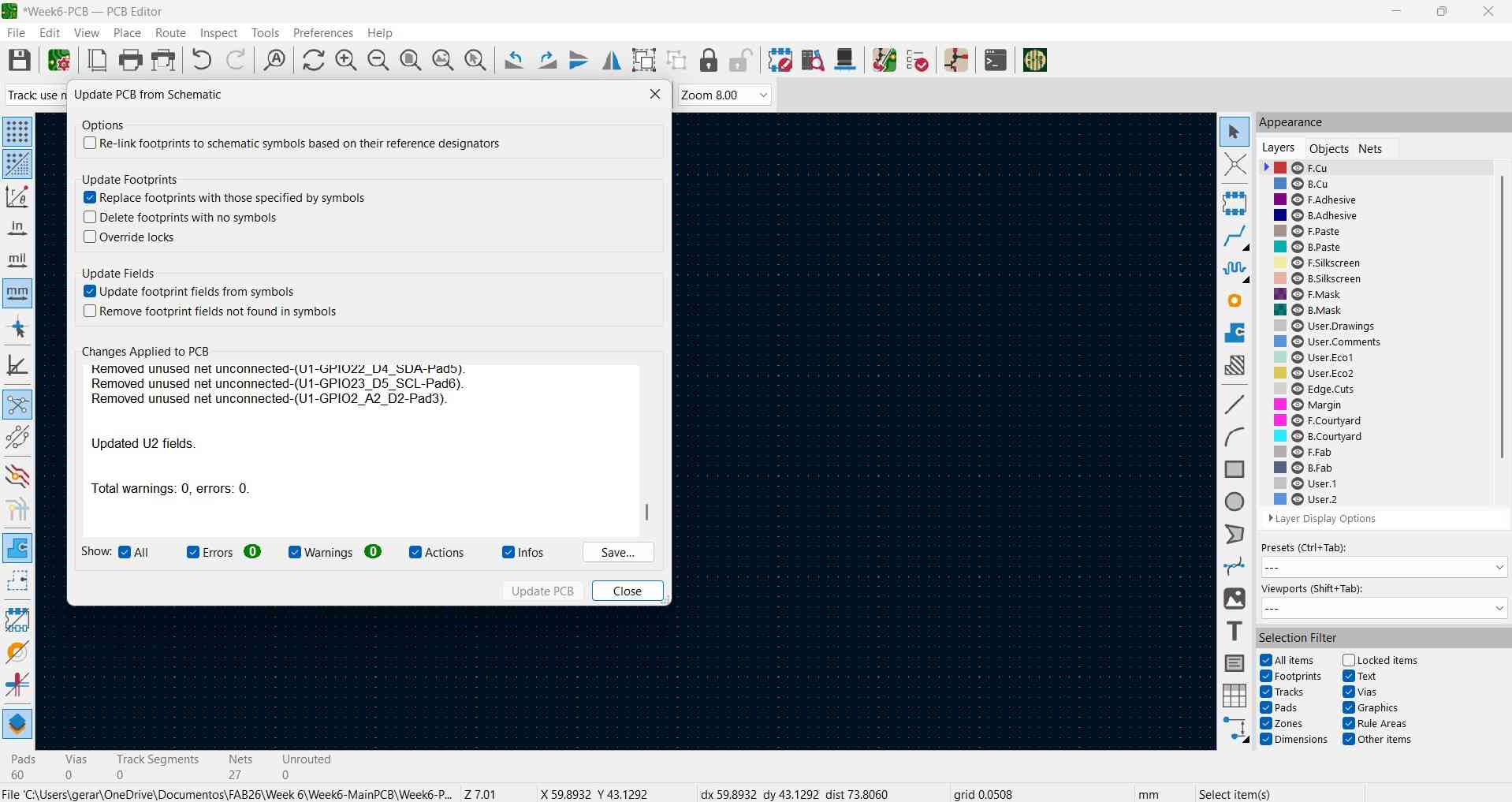
We can update our PCB from the schematic by clicking the fifth icon on the right side of the top toolbar. This operation imports the connections between components and can be performed whenever there are changes to the schematic.
I determined the track width using the calculator tool offered by KiCad on its main interface. As I expect my board to run at 1 ampere, the calculated trace width for this current falls well within the 0.8 mm limit set by the V-tool. This parameter can be applied to the connection lines by double- clicking on them and changing their width value.
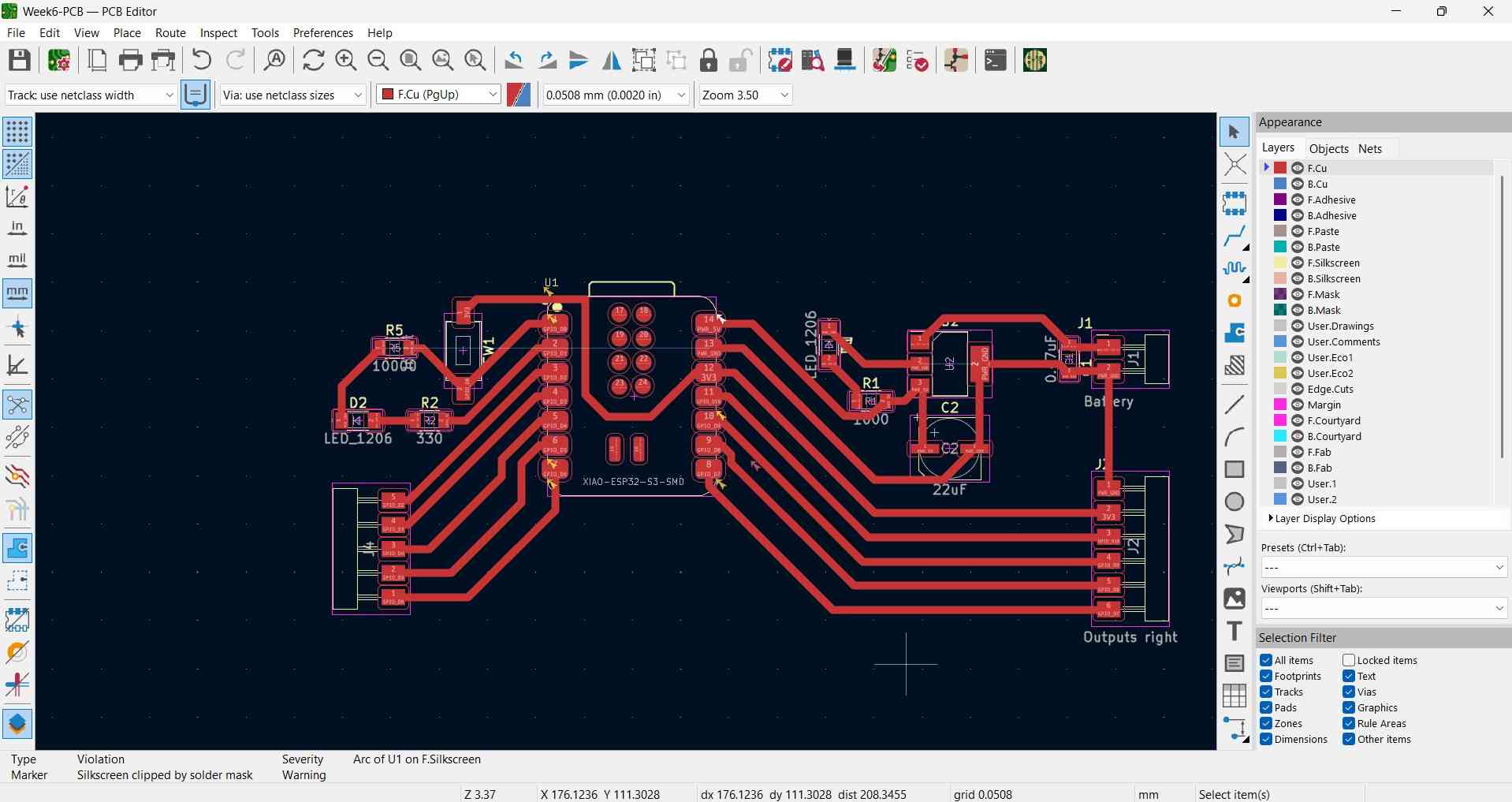
An important step in determining the shape of a PCB is drafting the edge-cut layer. After switching to this layer, I outlined my PCB shape using lines that are 2mm wide. This measurement corresponds to the cutting tool commonly used during the outline milling process at FabLab Ibero Puebla.
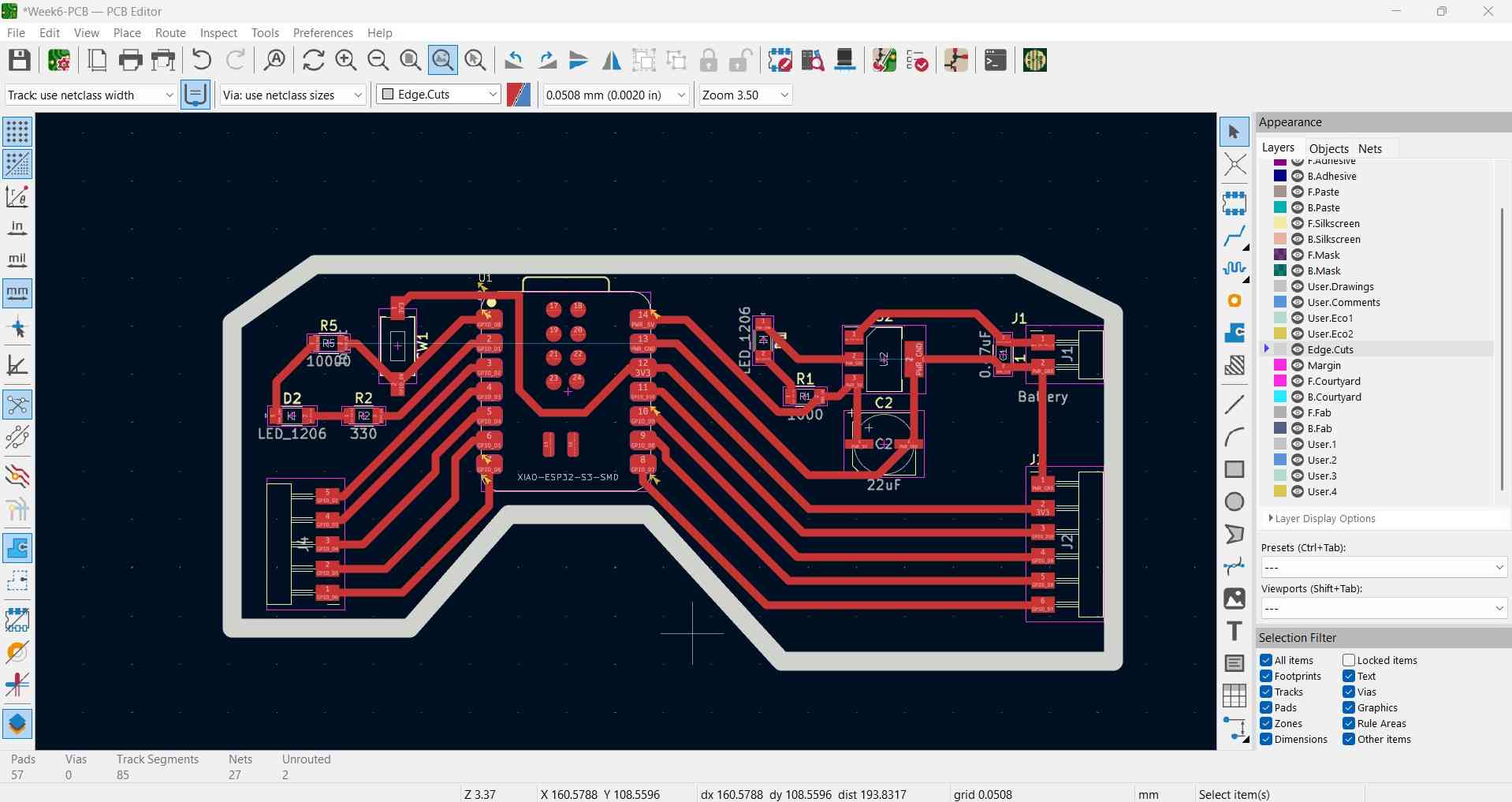
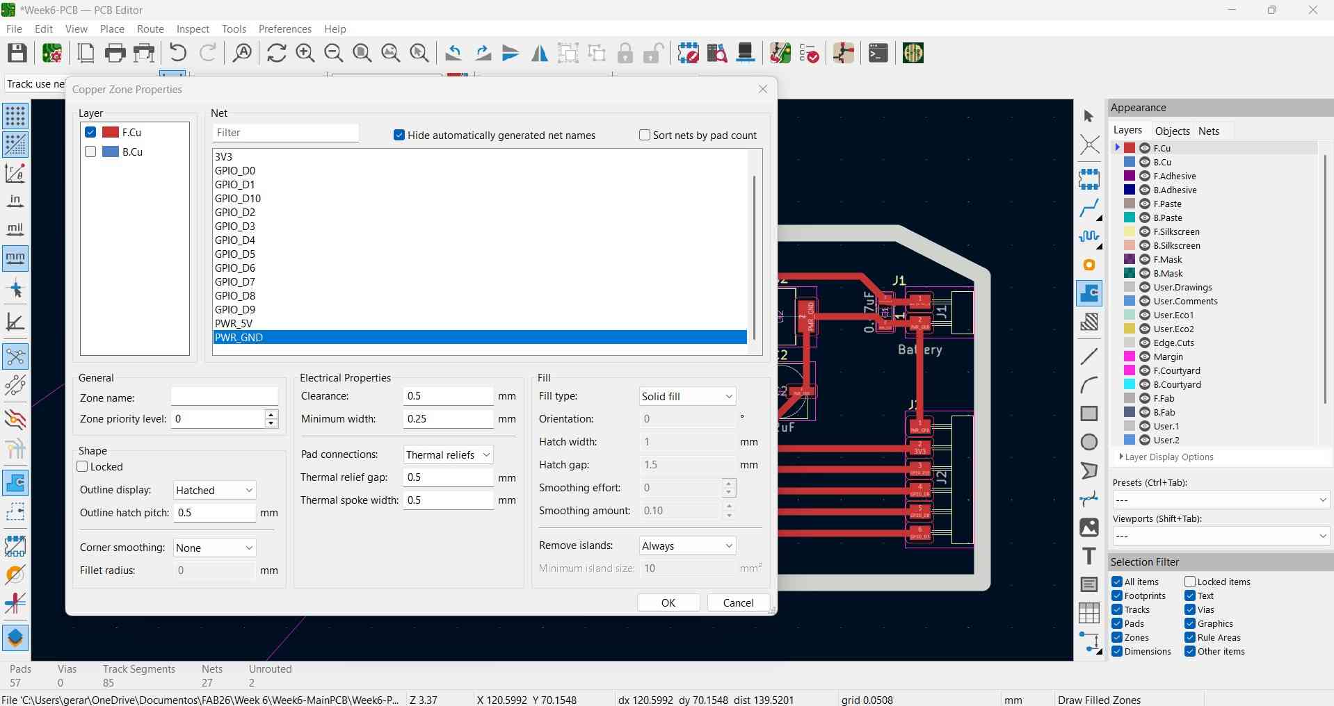
I also applied a copper pour to this PCB by using the copper zone tools. A copper pour is a large area of copper connected to a net like GND, creating a low-impedance return path. Copper pours can also assist with heat dissipation and noise reduction, and, in my personal experience, they can also reduce milling time. KiCad requires the user to repeat a similar shape to that of the edge-cuts layer to effectively apply the copper pour.
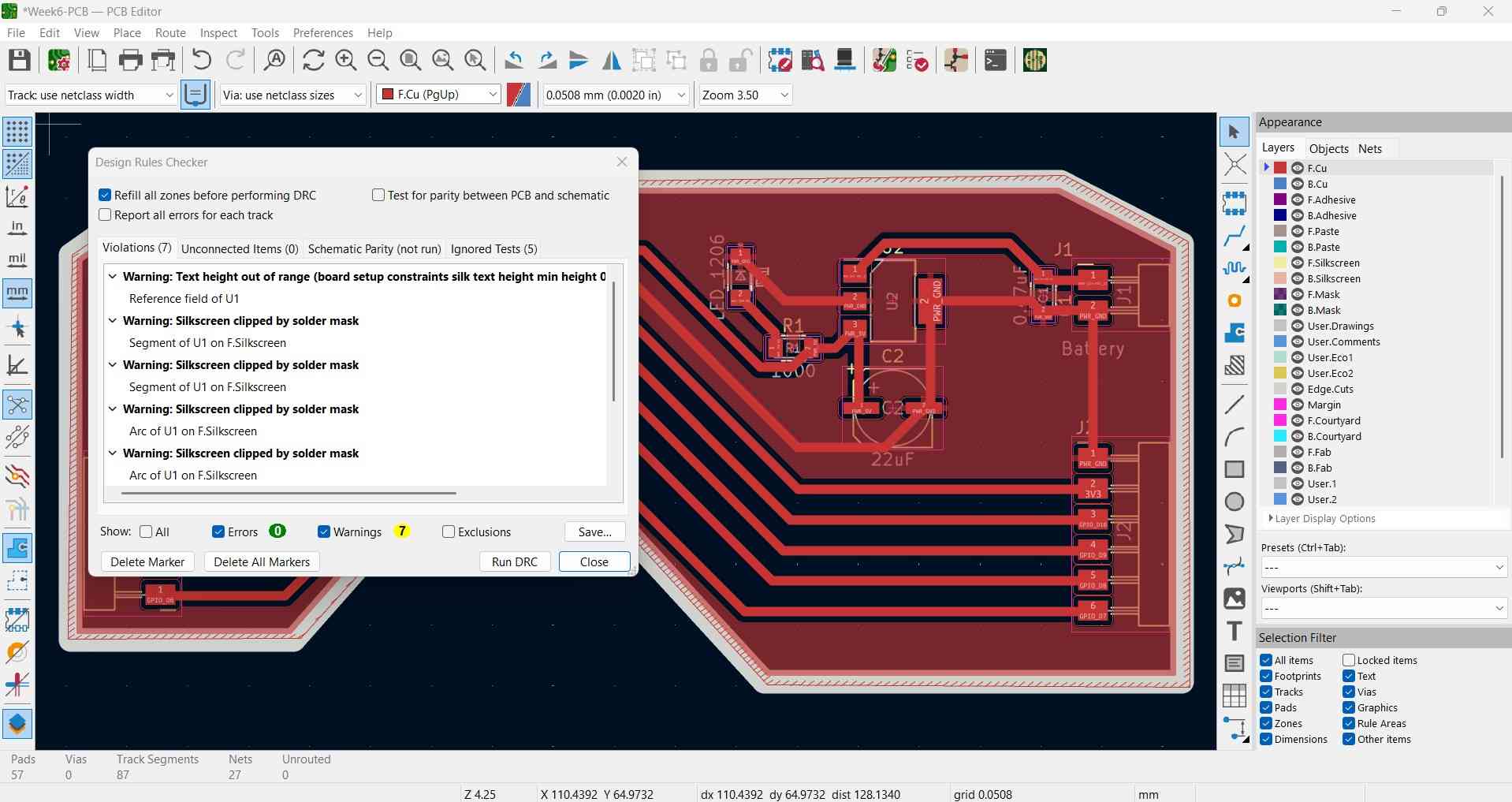
I executed the Electronic Rules Checker in conjunction with my schematic design. This time, I did not encounter any mistakes, only warnings. This indicates that my board can be manufactured as originally designed.
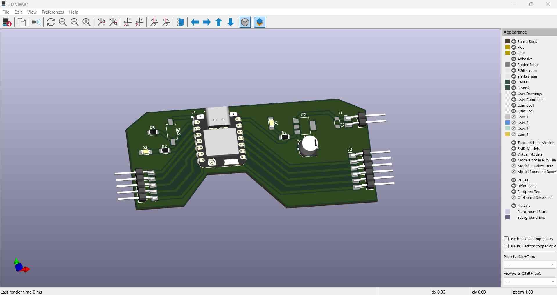
3D model of my PCB design
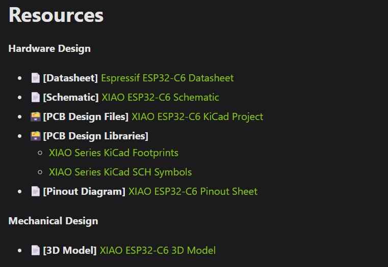
5. Files
Here are the downloadable files for this week:
KiCad schematic and PCB layoutReflection
While some ideas must initially be drafted by hand, such as circuit designs, it is advantageous to live in the era of EDA (Electronic Design Automation) software. I was previously unaware of the compatibility between EDA software and 3D CAD files; this capability can assist designers in more effectively sizing the spaces for housing electronics within a product.