6. Electronics Design
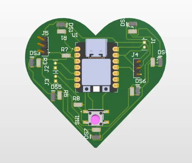
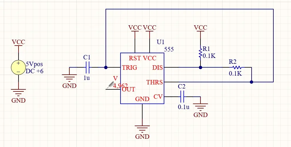
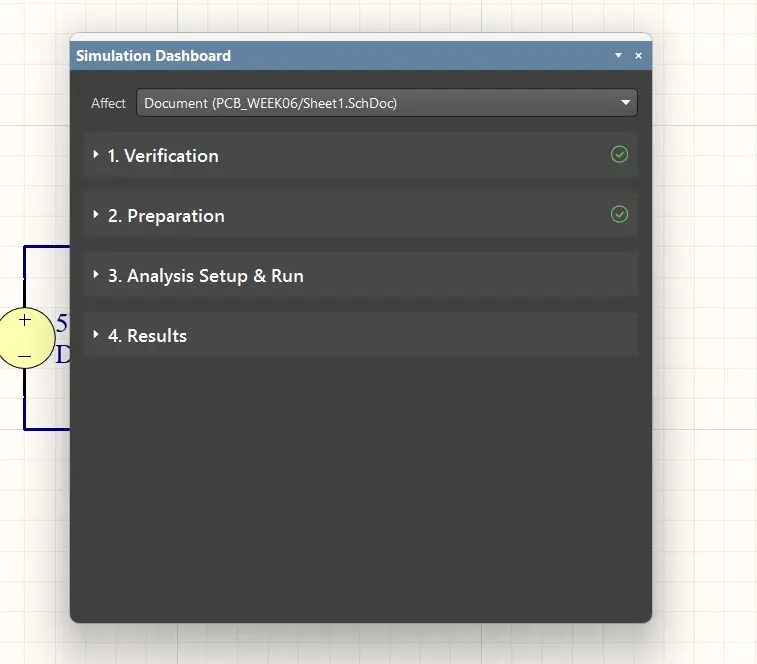
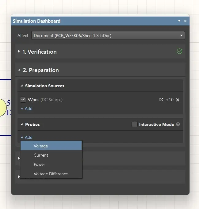
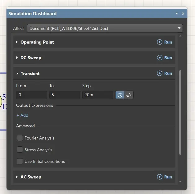
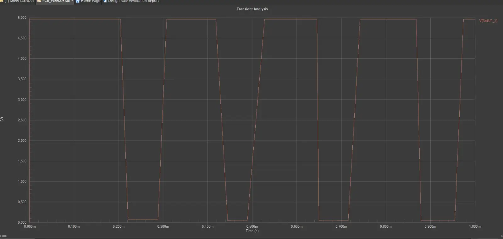
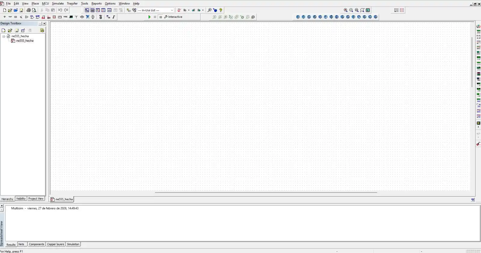
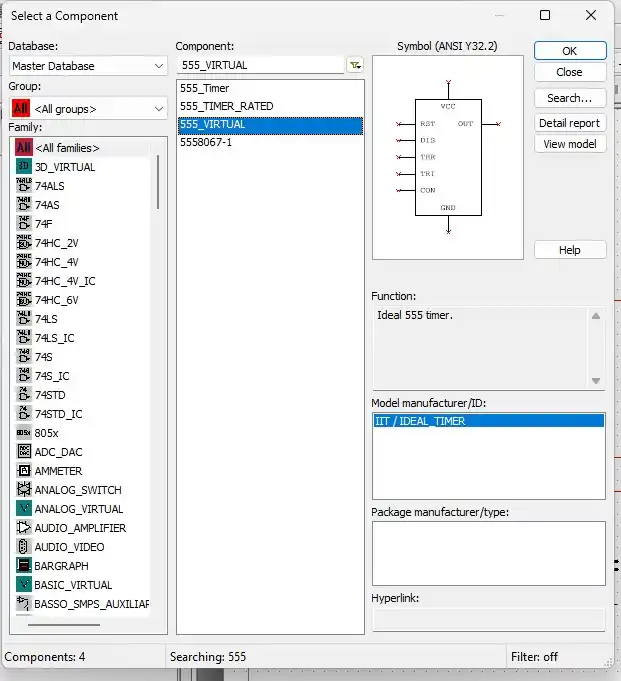
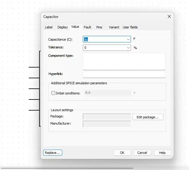
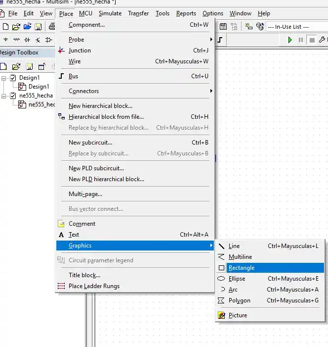
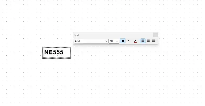
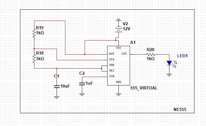
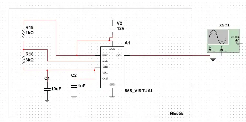
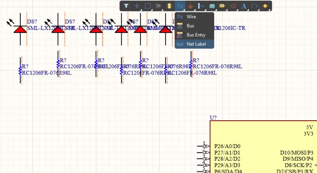
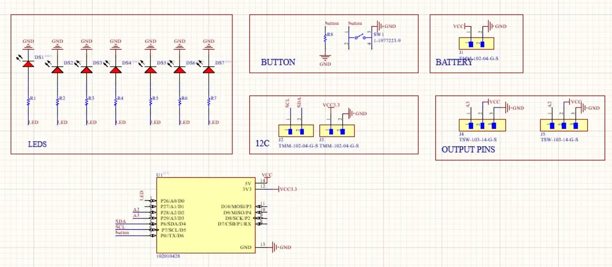
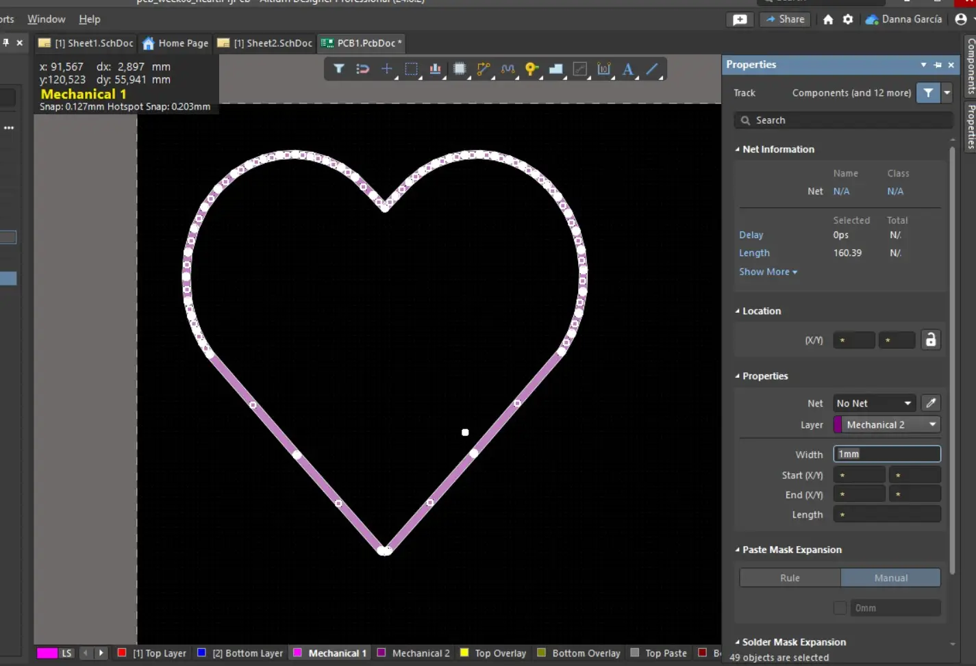
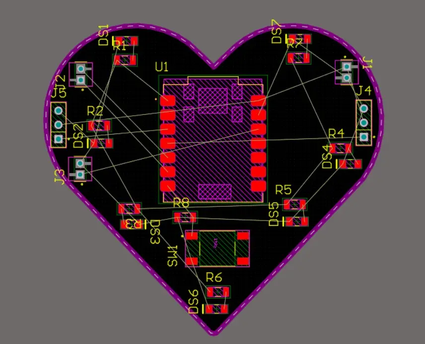
For this week's assignment, I simulated a 555 timer in Altium and Multisim. I also created a PCB in Altium that includes a button, I2C communication input pins, programmable LEDs, battery pins, and output pins (one connected to an analog pin and the other to a digital pin).
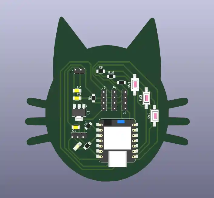
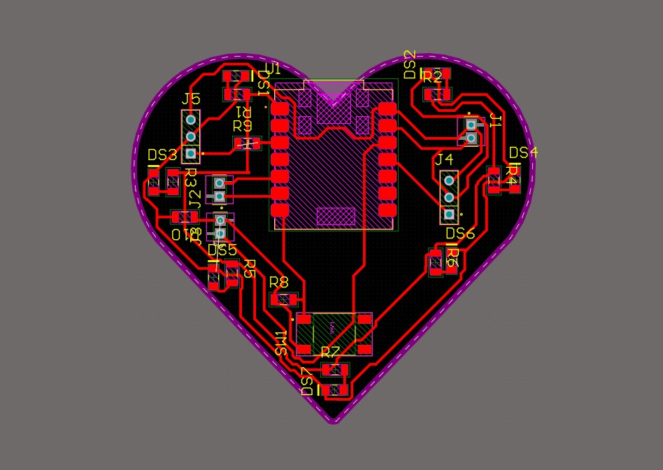
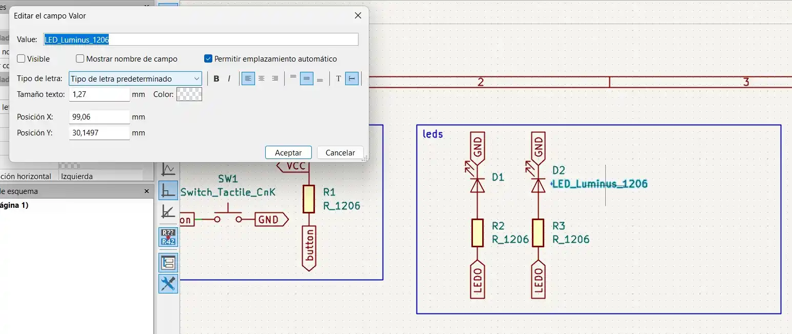
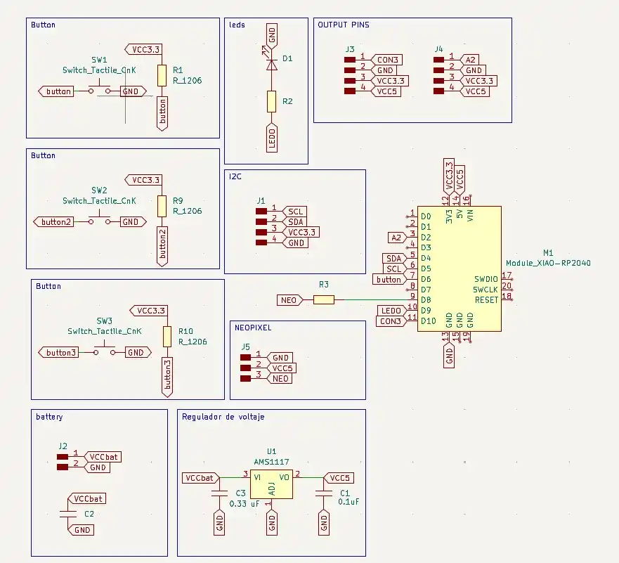
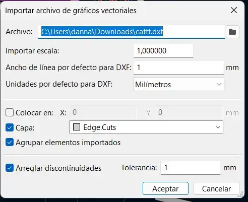
The PCB I created in KiCad has three buttons, an LED, battery pins, a 9-to-5V voltage regulator, I2C communication input pins, and output pins (one connected to an analog pin and the other to a digital pin). Finally, I added output pins for connecting a NeoPixel ring. Both PCBs are designed to accommodate a XIAO.
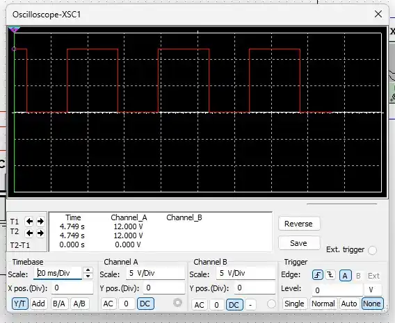
To see how we used the test equipment in our lab to observe the operation of an embedded microcontroller, visit our GROUP PAGE.
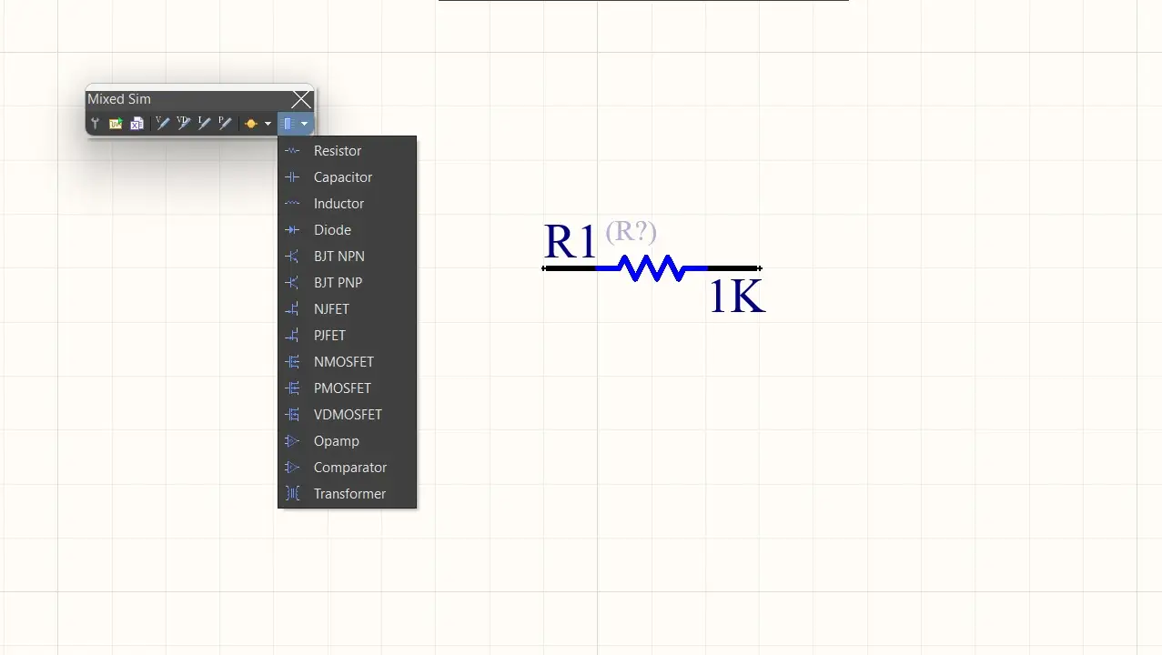
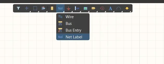
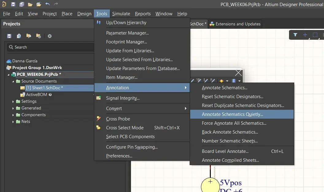
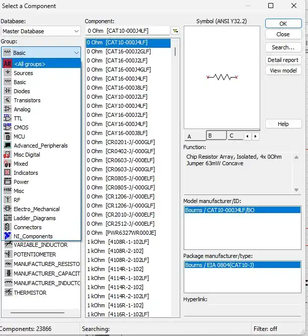
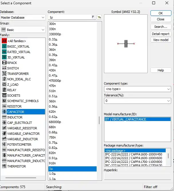
1. Simulation
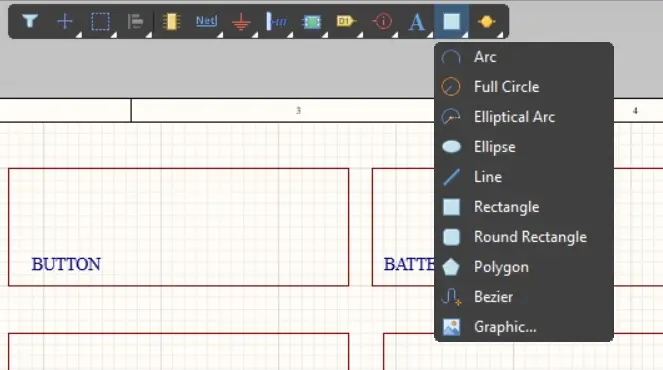
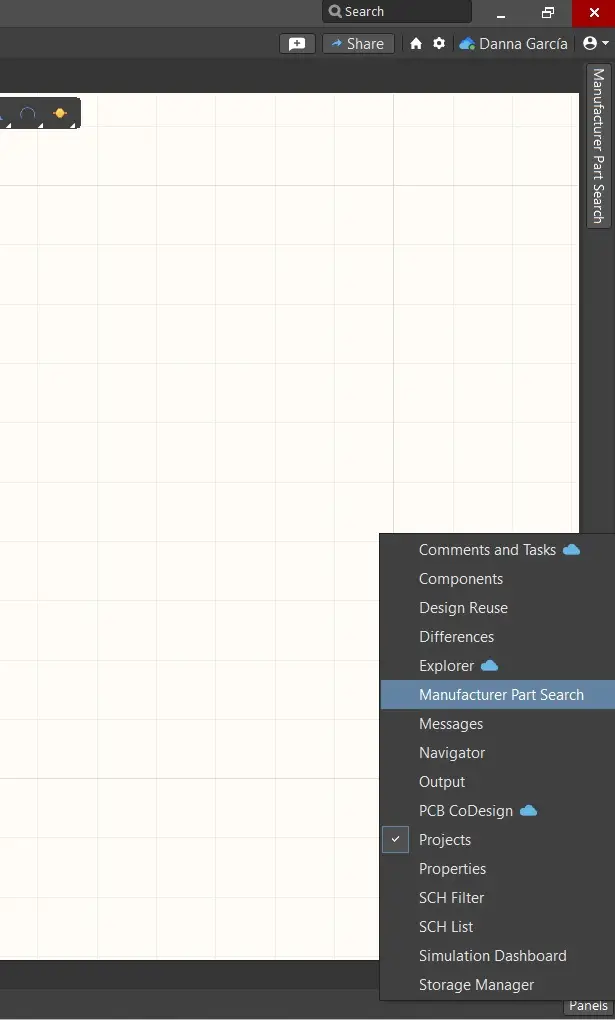
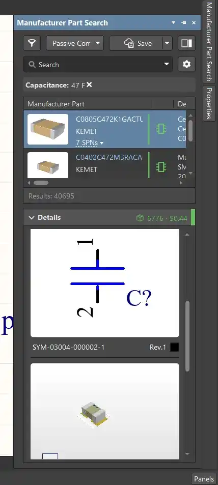
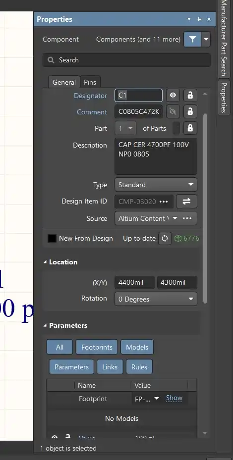
2. Design
| Key / Shortcut | Action |
|---|---|
| 2 | View 2D layout. |
| 3 | View 3D layout. |
| Ctrl + W | Start routing (Interactive Wiring). |
| Spacebar | Rotate component or footprint. |
| Q | Toggle units (mm / mils). |
| V + F | Fit board in screen. |
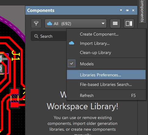
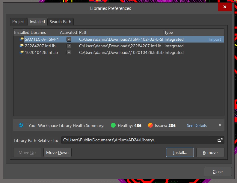
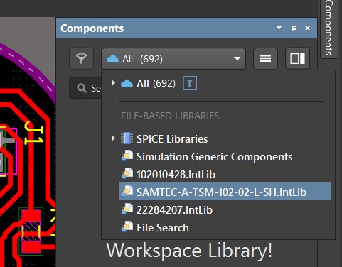
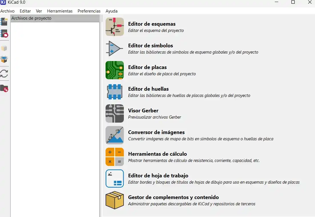
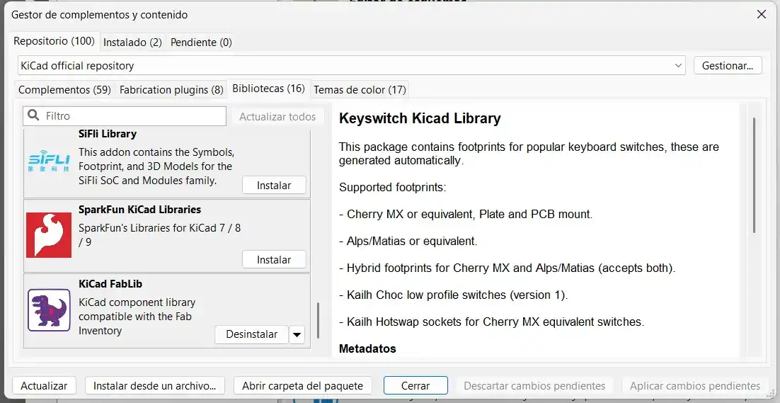
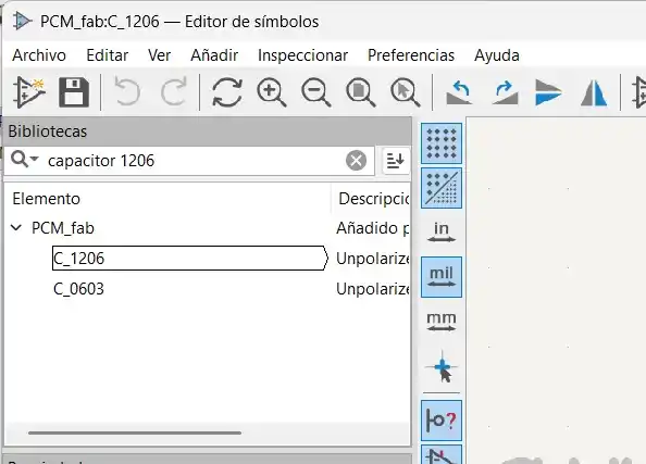
Adding Custom Libraries
PCB Process
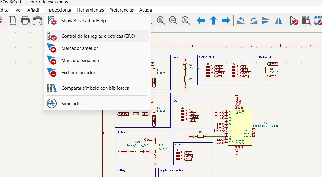
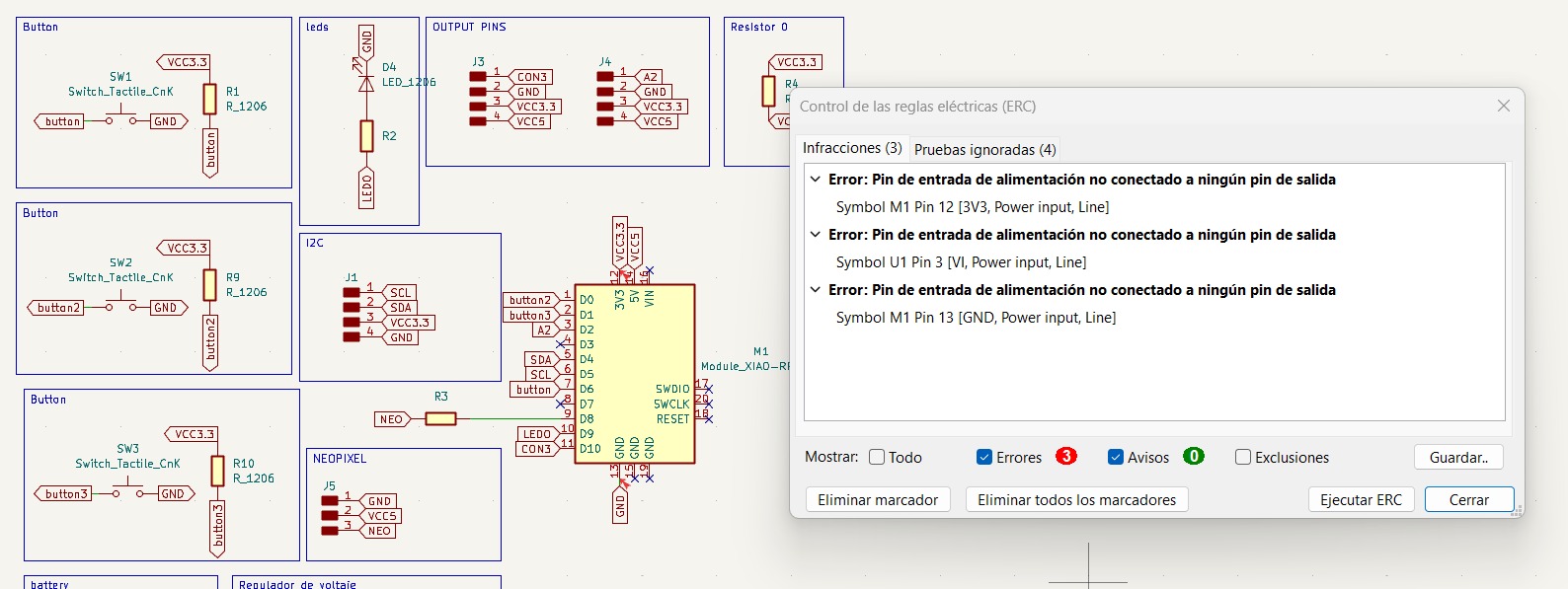
3. Results