Introduction
Group Assignment
Using lab test equipment — including a logic analyzer — to observe and document the operation of a microcontroller circuit board.
Group PageSoftwares
| Software | Use |
|---|---|
| KiCad | This is the one I used for this week. It is a free and open-source software, highly popular in the maker community and Fab Academy. It is used for schematic design and PCB layout without licensing restrictions. |
| Altium | It is a professional paid software that is the industry standard. It is used for high-complexity designs (multilayer, high-speed signals) and offers advanced simulation tools and component management in enterprise environments. However, it has a student version and the university has a license. |
Components used
Below I show the table with the board components and how I searched for them to add them.
Note: Be careful, as not all components have a footprint, so I added them but this was done in a later step.
| Component | Use | Name in KiCad | Footprint |
|---|---|---|---|
| XIAO-RP2040 | It is the microcontroller | Module_XIAO-RP2040 | PCM_fab:SeeedStudio_XIAO_RP2040 |
| Button | These are the buttons that will turn the LEDs on and off. | Switch:SW_Push | Capacitor_SMD:C_1206_3216Metric |
| Capacitor | It acts as a noise filter and energy reservoir to stabilize the voltage supplied to the microcontroller. | Device:C | Capacitor_SMD:CP_Elec_3x5.3 |
| LED | These are the lights that will turn on. | Device:LED diode | Capacitor_SMD:CP_Elec_4x5.8 |
| Power | Power center — it essentially comes from connecting the XIAO via a USB-C cable. However, to tell the program where the power supply comes from, one is placed at the 3V3 output and another at our "Ground". | PWR_FLAG | None |
| Resistor | They work to let only the necessary energy pass through to the LEDs so they don't burn out. | R_1206 | PCM_fab:R_1206 |
As I already mentioned in the table, the microcontroller I used is the XIAO since it is the one provided by my university's node. To get a clearer picture, I consulted the XIAO RP2040 datasheet (RP2040 Datasheet: A microcontroller by Raspberry Pi.) from which I obtained the following information to better understand its use.
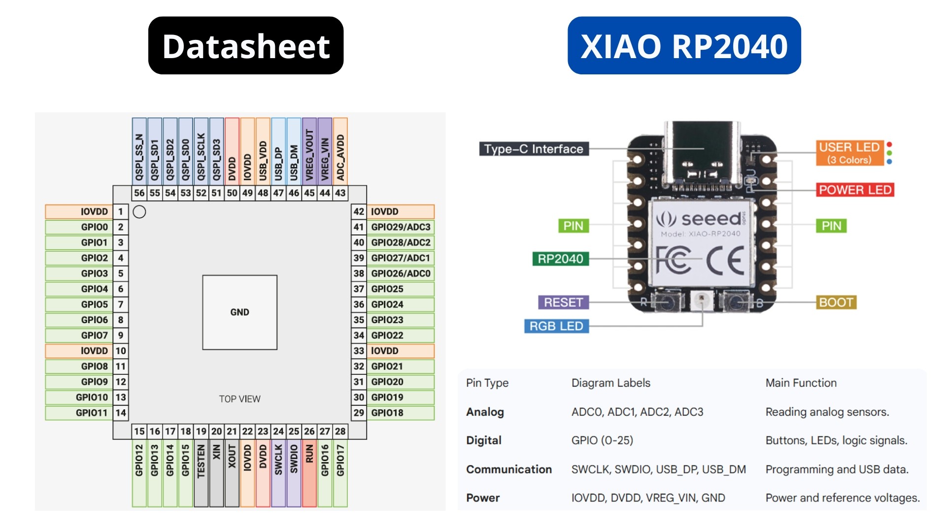
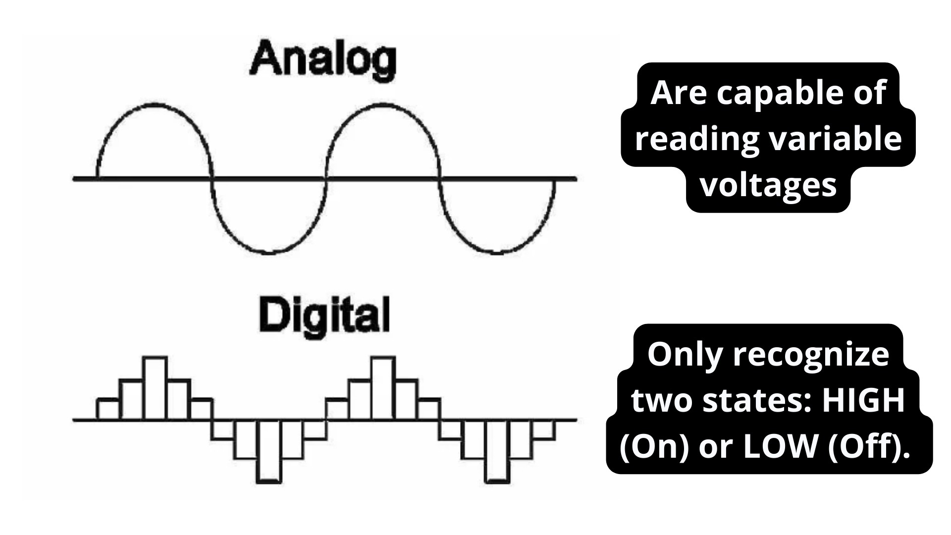
To understand the image above, it is important to know that there are two different types of pins: analog and digital.
Designing my schematic
Failed board (just a test)
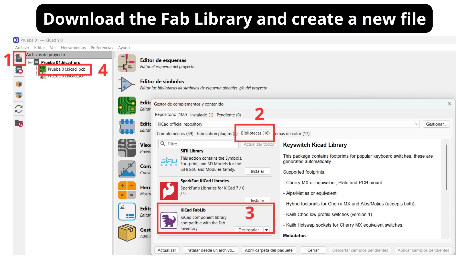
Creating a new file and libraries
The program I used is KiCad. The interface is shown in the image below. To get started, it is necessary to:
- Create a New document
- Go to the library section
- Search at the very bottom for the library called "KiCad FabIb" and install it.
- Afterwards, we can open the file by double-clicking on the "Schematic Editor" — the green symbol.
Place Symbols
To start adding symbols, click on the triangle symbol located in the toolbar on the right side of the screen. Another way to access the same menu is by pressing the "A" key on your keyboard.
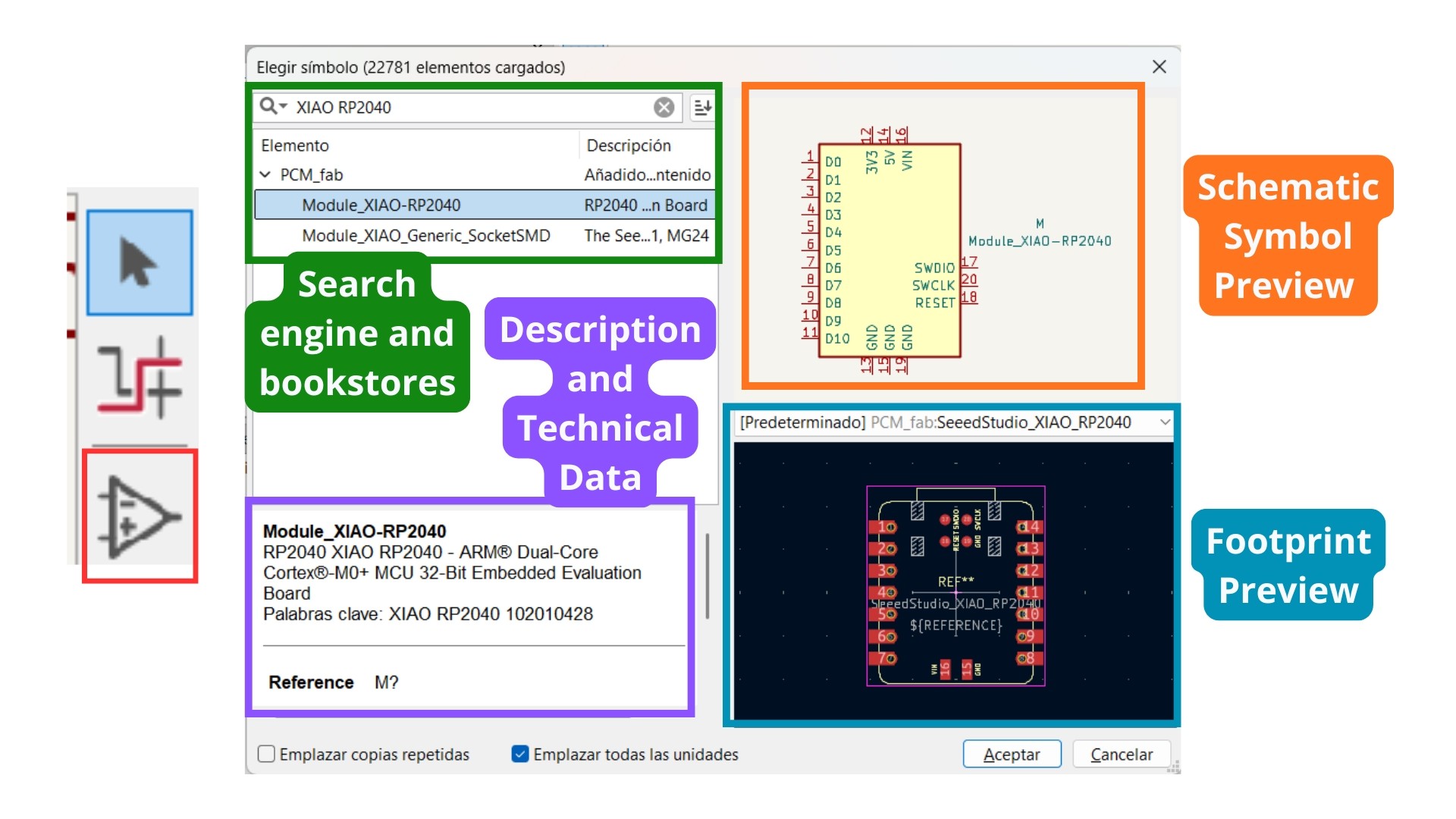
Commands “Place Symbols” parts.
Parts of the "Place Symbols" command:
- Search engine and libraries: Allows you to filter through thousands of components by typing their name (e.g., XIAO RP2040) and browse through installed libraries, such as PCM_fab.
- Schematic Symbol Preview: Displays the logical representation of the component, detailing pin names and functions to establish electrical connections in the diagram.
- Description and Technical Data: Provides detailed information about the hardware, including the exact microcontroller model, architecture (ARM Dual-Core Cortex-M0+), and keywords for identification.
- Footprint Preview: Shows the actual physical layout the component will have on the circuit board, including solder pad dimensions and the component's outline.
Start designing
The only notion I had when I started designing was that I needed buttons and a resistor connected to an LED. So I connected them the way I thought was right and then took a screenshot of my circuit to give the following prompt to the AI Gemini:
Prompt: "Is this correctly connected? What am I missing? My intention is for the buttons to turn on the LED."
For each modification I used the same prompt and uploaded the screenshot.
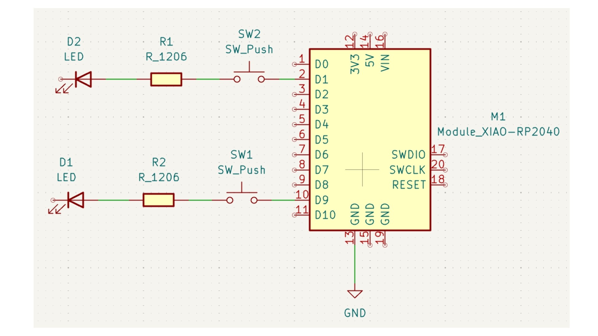
First sketch Screenshoot.
The three evolutions in the board design are shown in the image.
- First modification: I started using the "Labels" tool, which tells the program what is connected to what. This helps us avoid confusion with the wires and keeps the board more organized.
- I watched a YouTube video (Build a KiCad Project Schematic | Part 1) to learn how to correctly connect the buttons — that's where I discovered that capacitors need to be added to the circuit.
- Finally, I had to label the pins to which the components need to be connected.
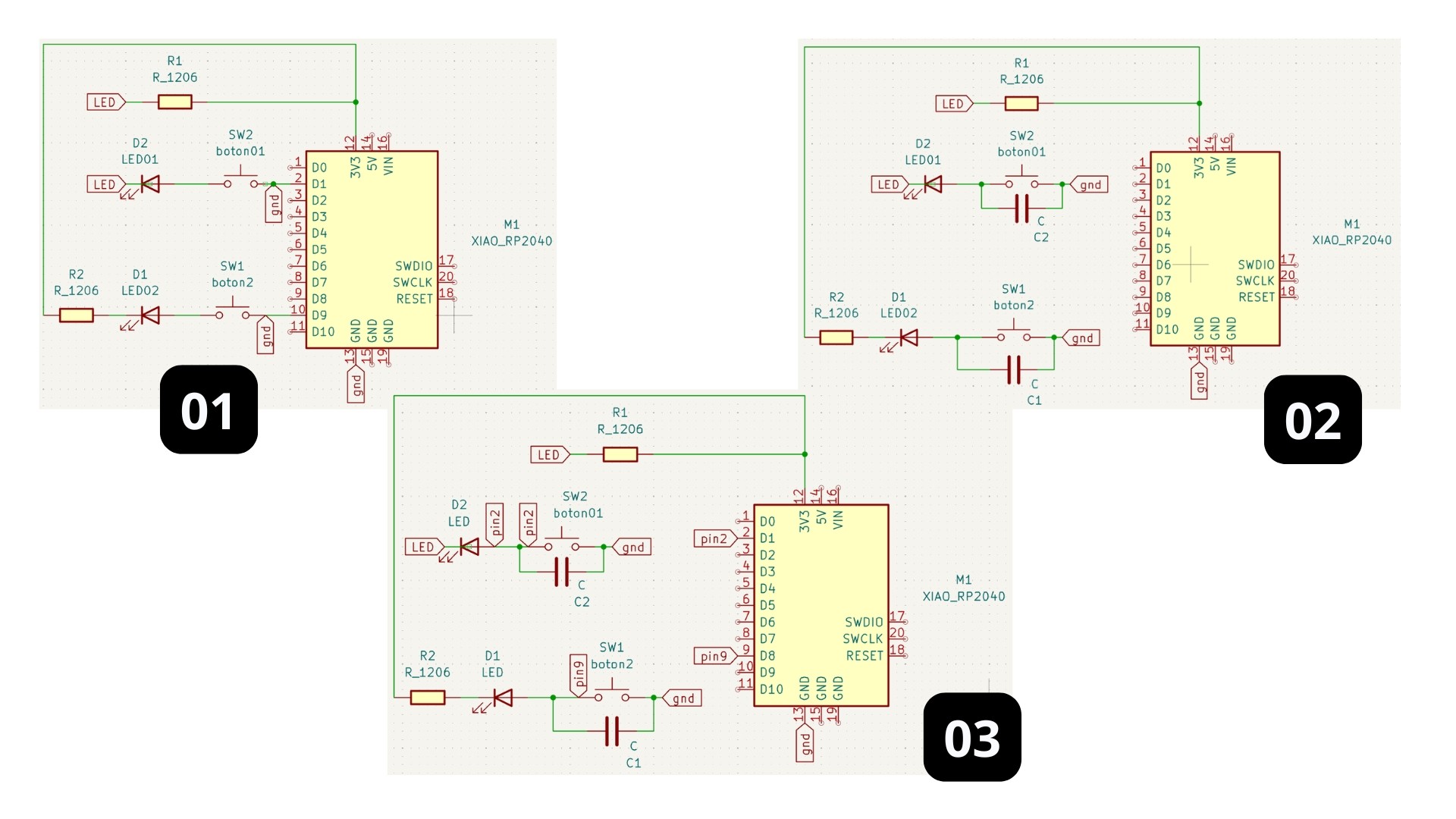
Three design evolutions.
Recommendation: To make it easier to organize the components on the board, I suggest naming each component in the side menu on the left of the workspace under the "Text" section.
Detecting errors in the design
Before moving on to the next process, it is important to check for errors in the board. To do this, use the tool under Inspect > Electrical Rules Checker (ERC). Then click "Run ERC" to run the diagnostic.
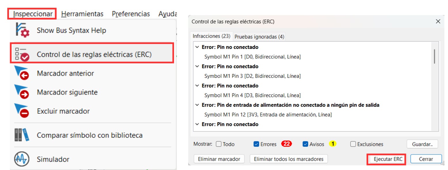
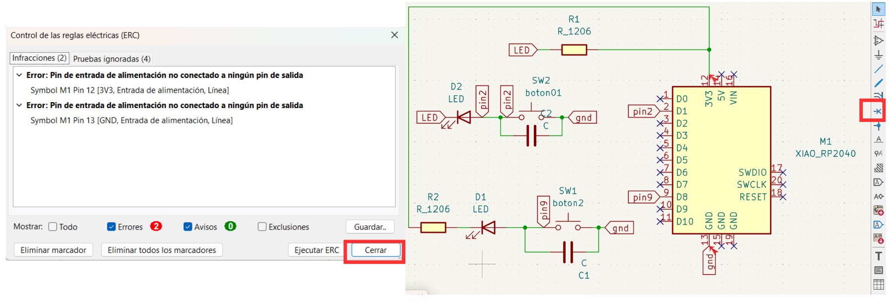
In my case, I had many pins that were not connected to anything, which flagged as errors. To fix this, I used a toolbar tool called "Place No Connect Flags", placing an X mark on all the XIAO pins that were not going to be connected.
Finished first draft of the board.
Note: This board did not actually work; however, it helped to understand how KiCad works.
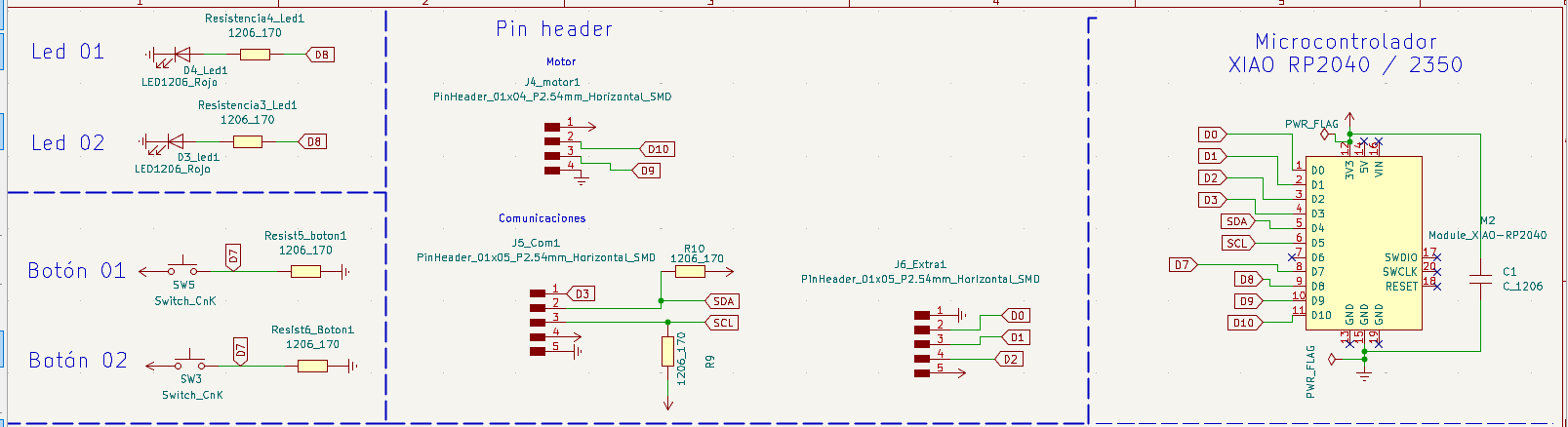
Final main board
KiCad
Component List
| Resource (Component) | Description / KiCad Search Term | Format / Link |
|---|---|---|
| Main Controller | Seeed Studio XIAO RP2350 (Compatible with RP2040 Footprint) | Datasheet |
| LED Indicators | Red LED 1206 — Status and feedback indicators (Qty: 2) | PDF Document |
| Capacitor | C_1206 — Ceramic Capacitor for power stability | PDF Document |
| Resistors | R_1206 — 170Ω Resistors for LEDs and Buttons (Qty: 6) | SMD 1206 |
| Motor Connector | 4-Pin Male Header (Horizontal SMD) — Stepper motor interface | Pin Header |
| Extra IO Headers | 5-Pin Male Header (Horizontal SMD) — Communication & Extra pins | Pin Header |
| Tactile Switches | C&K PTS636 — Push buttons for user input (Qty: 2) | PDF Document |
Schematic Editor
The board is designed to be modular, so it is made up of different parts:
- LEDs that will blink.
- Buttons that will be responsible for turning the LEDs on.
- Pin headers: one designed to connect a stepper motor, another to enable I2C communication, and extra pins to make the most of the XIAO.
- XIAO RP2350, which is our microcontroller.
I followed the same process as before and verified that there were no errors using the Inspect > Electrical Rules Checker tool.
Board
Importing the design
- In the same schematic editor, click on the "PCB Editor" icon — the green one at the far right of the top toolbar.
- Import the schematic using the button.
- Add footprints to the missing components (which was the error flagged in my case). To do this, click on the component to select it and press the E key on your keyboard to open the menu. Then click on the marked icon shown in the image and search for the component name (the ones I listed in the first table of my documentation).
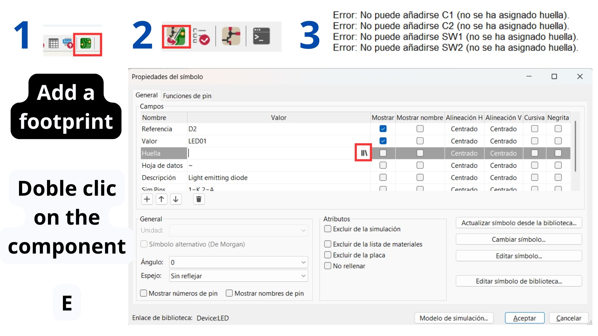
First way to assign a Footprint.
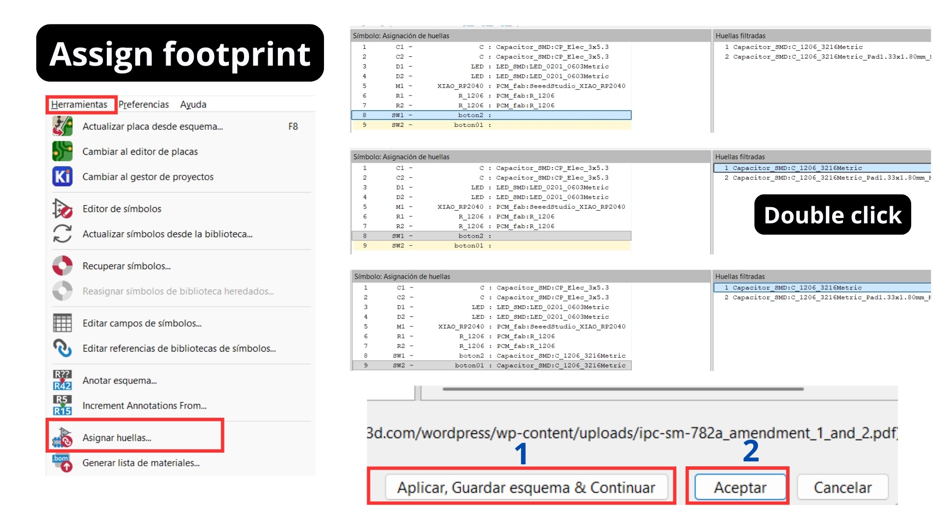
Second way to assign a Footprint.
Layers
The layers I recommend keeping visible are the following:
- F.Cu (Front Copper): This is the top copper layer where you route the electrical traces and place the surface-mount (SMD) pads.
- B.Cu (Bottom Copper): This is the bottom copper layer, used for routing traces on the back of the board or for creating ground planes.
- F.Silkscreen (Front Silkscreen): This layer contains the white ink printed on the top of the board, used for component outlines, logos, and reference designators like "R1" or "C1".
- F.Mask (Front Solder Mask): This layer defines the areas on the top side that should NOT be covered by the protective epoxy coating (solder mask), exposing the copper for soldering.
- Edge.Cuts: Although not highlighted in your text but visible in the list, this critical layer defines the physical boundary or "cut-out" shape of your PCB.
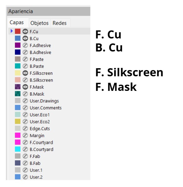
Layers panel in KiCad.
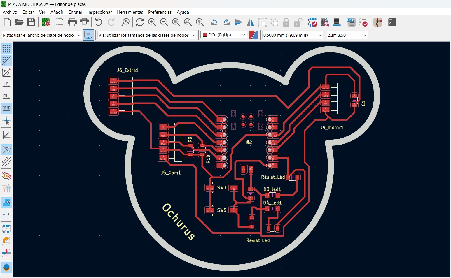
Board layout
All components must be arranged so that the blue lines do not cross each other.
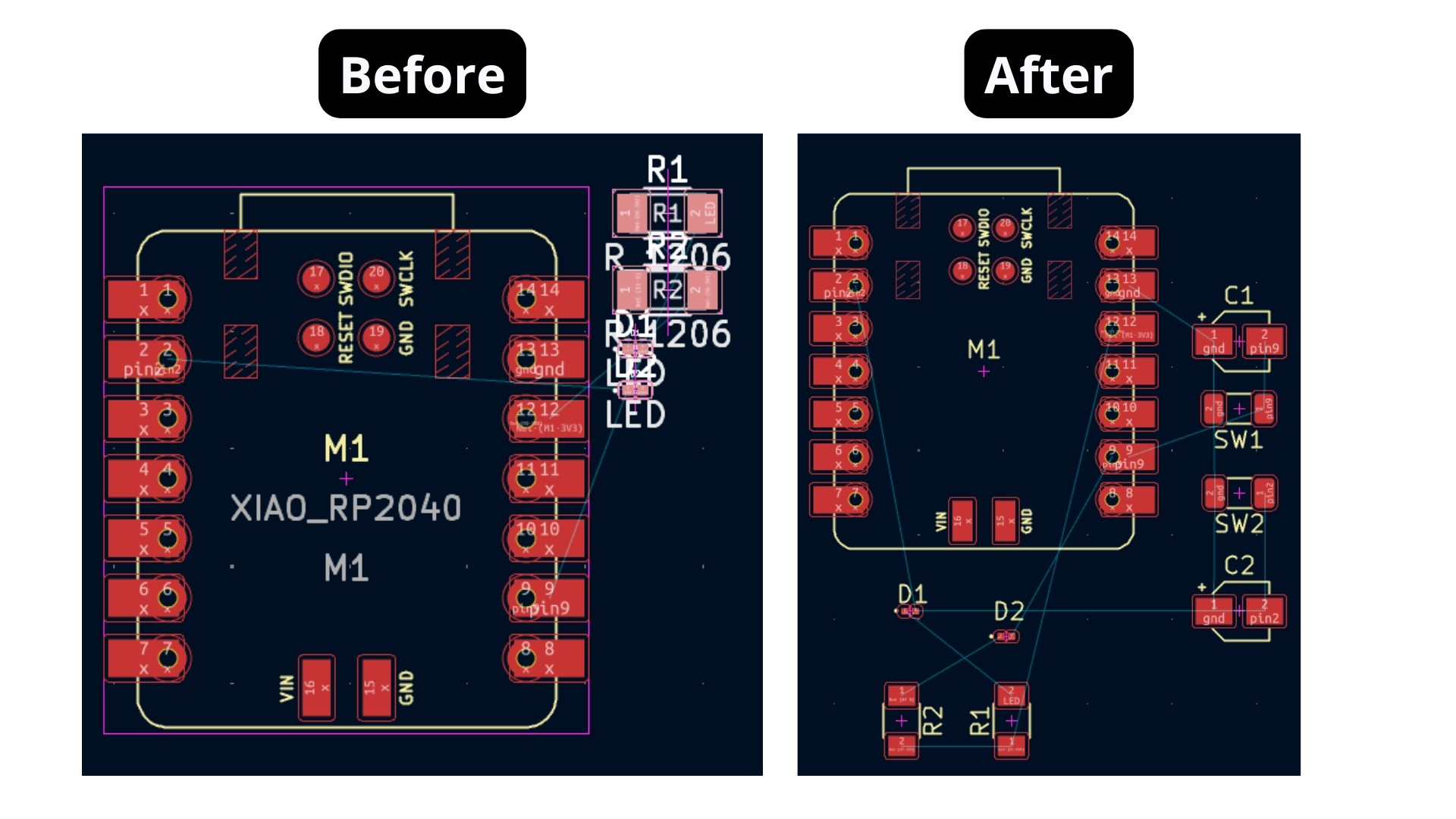
To wire the components together, use the "Route Single Track" tool. The only rule is that no tracks should cross, which is why the previous step — ensuring the blue lines don't cross — is so important.
It is important to configure the track width on the board. To determine the "Minimum track width" (calculated with the KiCad calculator), I used the following prompt in Gemini.
Prompt: How many amps do I want my circuit current to be, to enter it into the KiCad calculator?
With the information Gemini gave me, I moved to the KiCad calculator where the only things I changed were the current and the maximum temperature my PCB can reach. As a result, my "Minimum track width" should be at least 0.115 mm — I exceeded this by a lot, so it's fine.
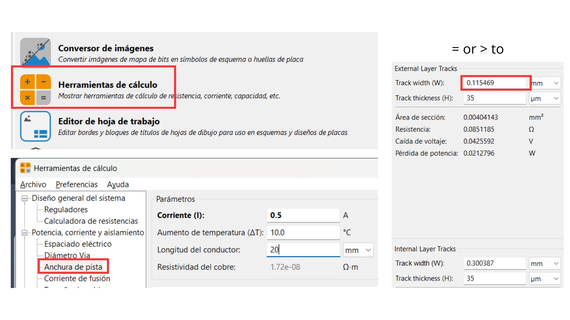
Minimum track width in KiCad calculator.
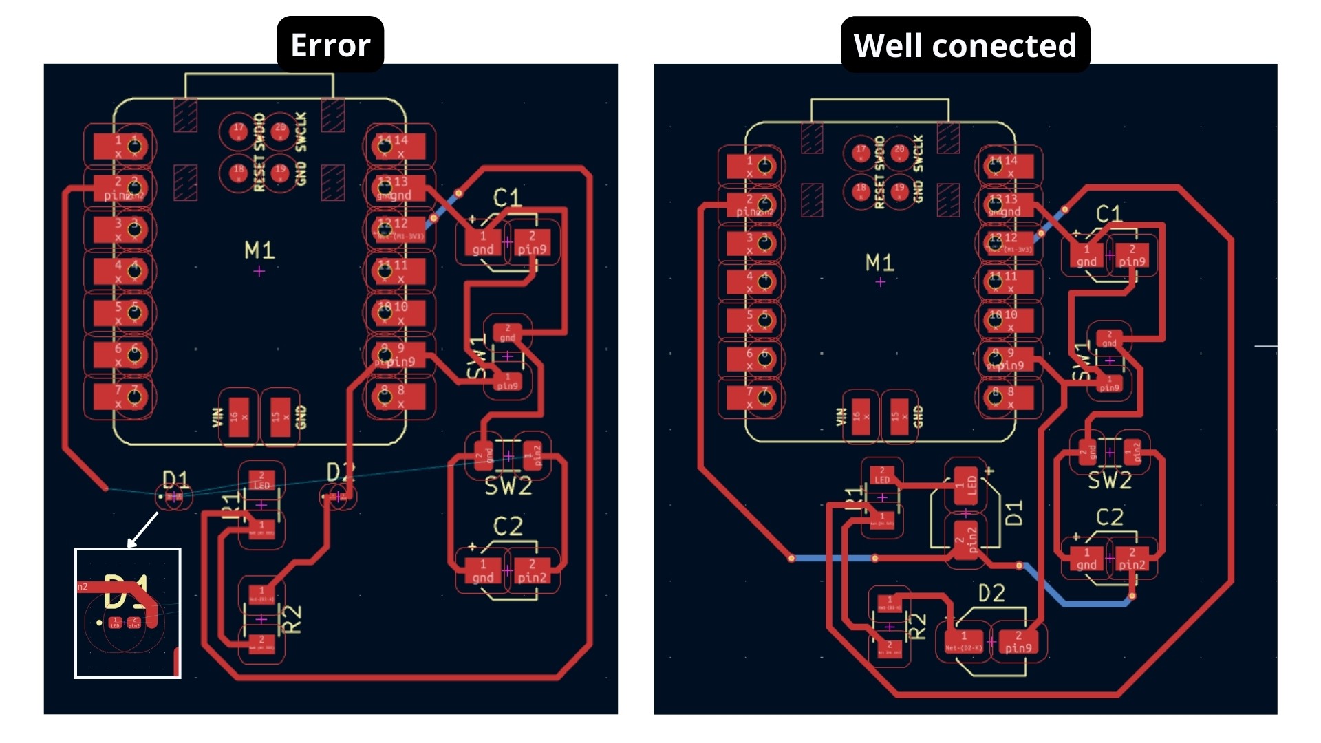
Watch out for this error: When I tried to connect the LEDs (shown as D1 on the board), the routing path was too large and merged with the other leg of the LED, which prevented me from making the connection. To fix this, I switched to a larger LED so I could connect it without causing a short circuit on the board.
Note: I used the V command on the keyboard to route the track underneath the board. However, be careful when manually flipping the board before sending it to be physically made — it must remain in the same flipped position so that it aligns correctly with the other side.
Routing underneath the board using the V command.
Additionally, use the "Draw Lines" tool to draw the board outline.
Note 01: This line appears in the right toolbar as a grey line instead of a blue one, like the one found above it.
Note 02: You must be on the correct layer — for the external cutout, it is Edge Cuts. I realized this error once I ran the error check.
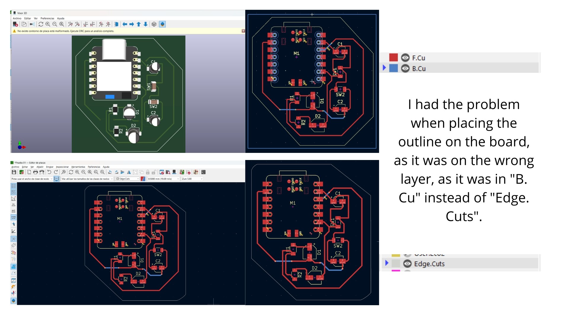
Board outline on the Edge Cuts layer.
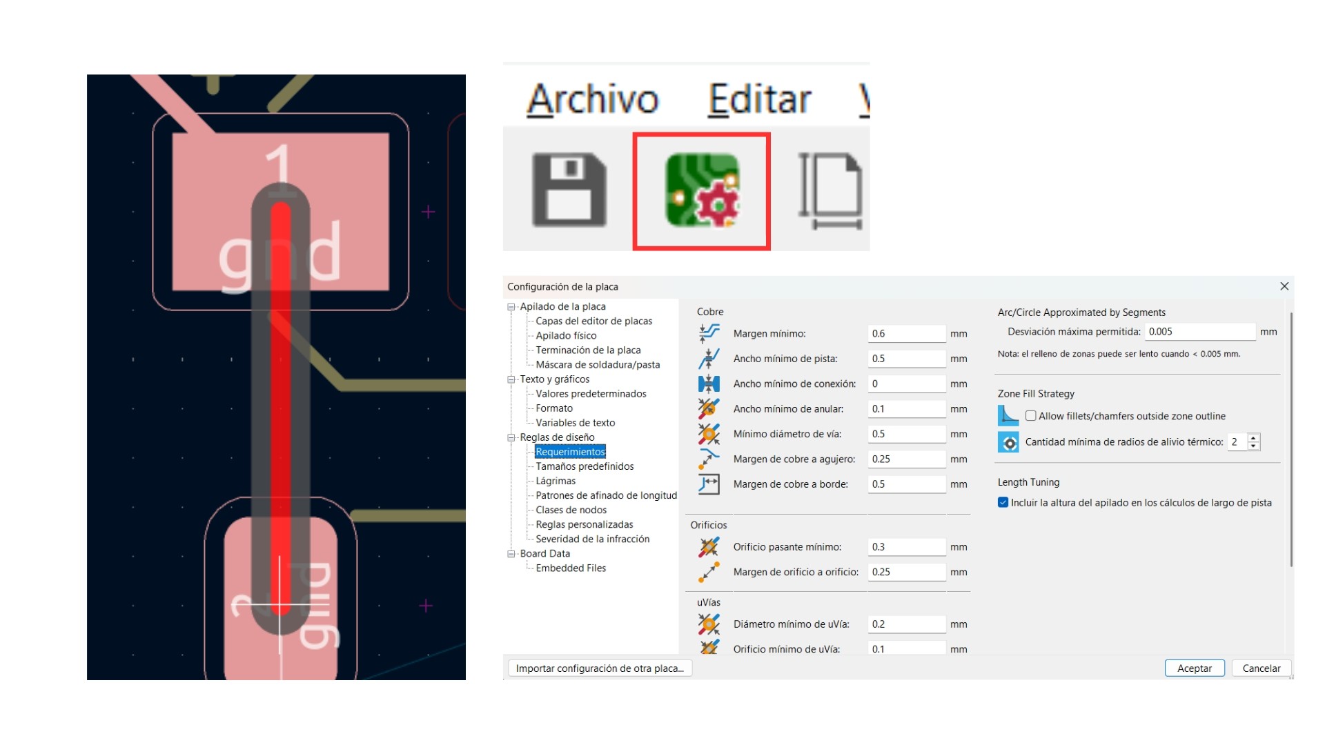
Detecting errors
Just like in the schematic design, you need to check for errors. Go to the Inspect > Design Rules Checker > Run DRC tab.
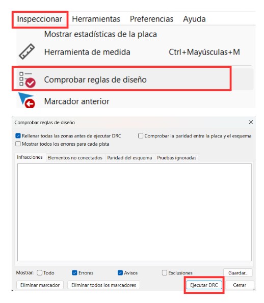
Design Rules Checker window in KiCad.
Viewing in 3D
Once the errors are corrected, go to the View > 3D Viewer tab to see your model.
Saving your file
- Go to File
- Select the "Export" option
- Click on STEP, so you can modify it in the program you need.
Final main board
Board Editor
I made the pads with the following specifications.
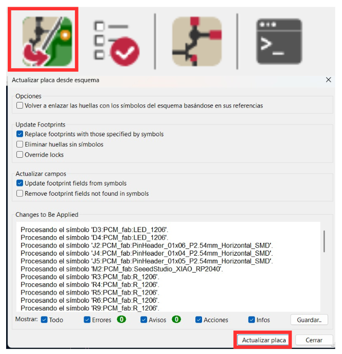
Note: I made the pads and realized I had to make multiple changes to make it easier to connect them. Therefore, an important step: whenever a change is made in the schematic editor, it is important to import it and click the "Update PCB" button.
Additionally, I changed the border thickness (saved in Edge.Cuts) to 2mm. The final board looked like this:
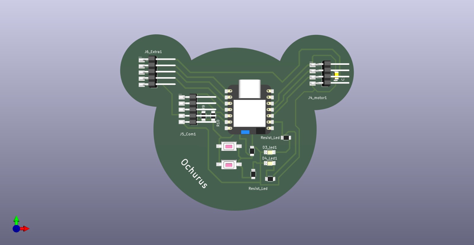
Final board in 3D — completed.
What I learned this week:
- I consider PCB manufacturing to be one of the most valuable tools because, ultimately, it is what is used to create electronic products today; therefore, it is the foundation of the current industry.
- I learned to translate an idea into a more professional format, moving beyond breadboard designs toward actual schematics and layouts in KiCad.
What I learned from the group page:
- I learned to use a multimeter to measure voltage (in parallel), current (in series), and continuity, and I understood why measured current may vary from the theoretical value due to real component consumption.
- I learned to use the oscilloscope to visualize PWM signals generated by the RP2040, identify the duty cycle, and measure pulse width with cursors to obtain precise readings.
- I understood how UART communication works and why the character "D" appears inverted on the oscilloscope (00100010 instead of 01000100) due to the protocol's LSB-First standard.
YouTube videos that helped me in this section
| Description | Link |
|---|---|
| General tutorial in Spanish | Kicad Tutorial en 10minutos |
| Summary of how to use KiCad (in English) | KiCAD 7 PCB Layout in 5 steps |
| How to correctly connect a button | Build a KiCad Project Schematic | Part 1 |
Files I used this week
w06_KiCad_files.zip
Failed Electronic Board Files
Los siguientes archivos están incluidos en el paquete:
- 01_First
- 02_Schematic_desing
- 03_Board
Ochurus_final_board.zip
Final main board
Los siguientes archivos están incluidos en el paquete:
- Placa modificada.kicad_pcb
- Placa modificada.kicad_prl
- Placa modificada.kicad_pro
- Placa modificada.kicad_sch