Electronics Production
On week 6 we designed our very first PCB. It is now time to bring it to life. Electronics production refers to the act of creating our designed PCB into its own functional product. This is usually one of the last steps taken on electronic driven projects. It might take 1 or 2 or more iterations, but in the end a well-crafted PCB is what we Makers aspire.
PCB can be manufactured in many ways. For more professional and formal work, exporting your design to a PCB manufacturer like PCBWay is ideal, as these types of companies will produce your PCB with industry-quality parts and machines to end up with something you might find inside any electronic product you can think of. For us makers, PCBWay is the very last step on the list. We need ways to make prototypes that not only work as intended, but are also cheap and fast to produce in house.
Upgrading Our Design
There are a few things I want to upgrade to our original design before printing it out:
- The trace width must be adapted to better fit the machine‘s drill bit size.
- I need to add a “Copper Ground Field” to my PCB (more on that later).
- I want to change the Symbol for the RP2040.
Changing the RP2040‘s Symbol
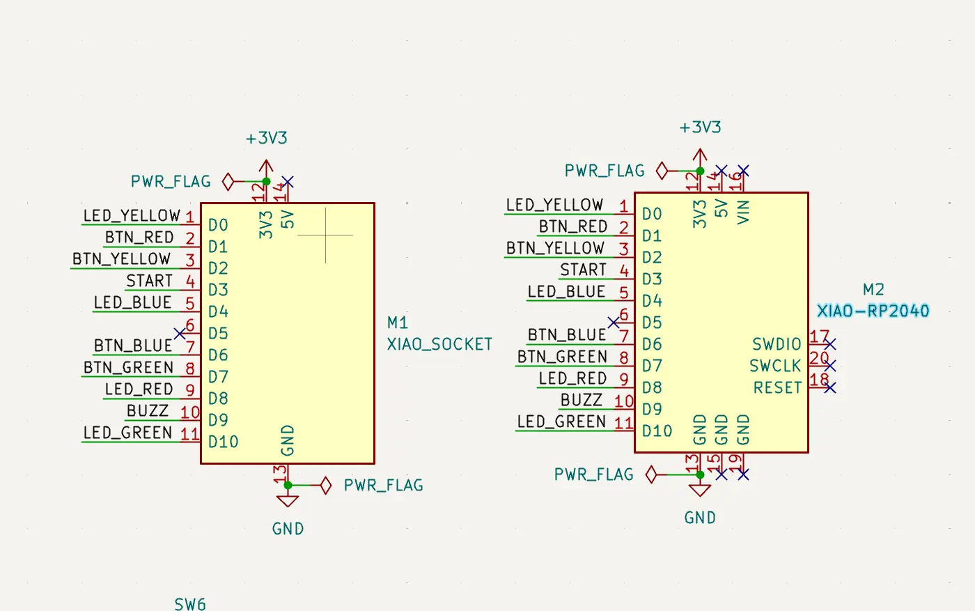
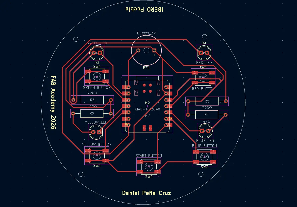
The first symbol of the RP2040 I selected was meant to be an special holding piece, where the actual RP2040 can be safely plugged in and out with out soldering. Unfortunately, we do not have access to that specific holding piece. So, the logical solution is to use the actual RP2040´s symbol and soldering its pins to the PCB. That way, the RP2040 can be placed and removed when the project is over.
To do this, I simply added the new symbol on the schematic editor and connected every pin to its corresponding label. There where a few extra pins on this symbol, but we can just ignore those for now.
Modifying the Traces
We need to make our traces a little bit bigger. The Roland uses a drill bit to cut the empty spaces, leaving only the actual traces in copper. Our current traces use KiCAD´s standard size, that are not optimized for our specific machine. But we can change our project´s setting, by going to File > Board Setup. In this menu, we can go to Design Rules > Net Clases to make our needed adjustments.
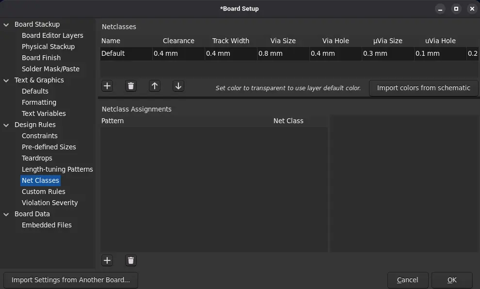
After doing some research, I decided to go with the following parameters:
- Clearance = 0.4mm
- Track Width = 0.8mm
- Via Size = 0.8mm
- Via Hole = 0.4mm
- Everything else as default
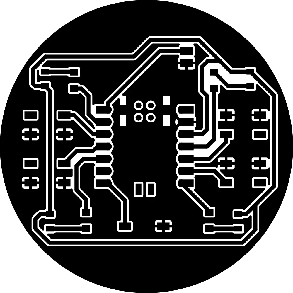
Now, we can update our PCB in the PCB editor to import the new RP2040 Symbol, and changing the tracks with our new sizes. I personally deleted the old layout to make a new design, I´m not sure if just changing the Net Clases values will automatically change the existing track´s size.
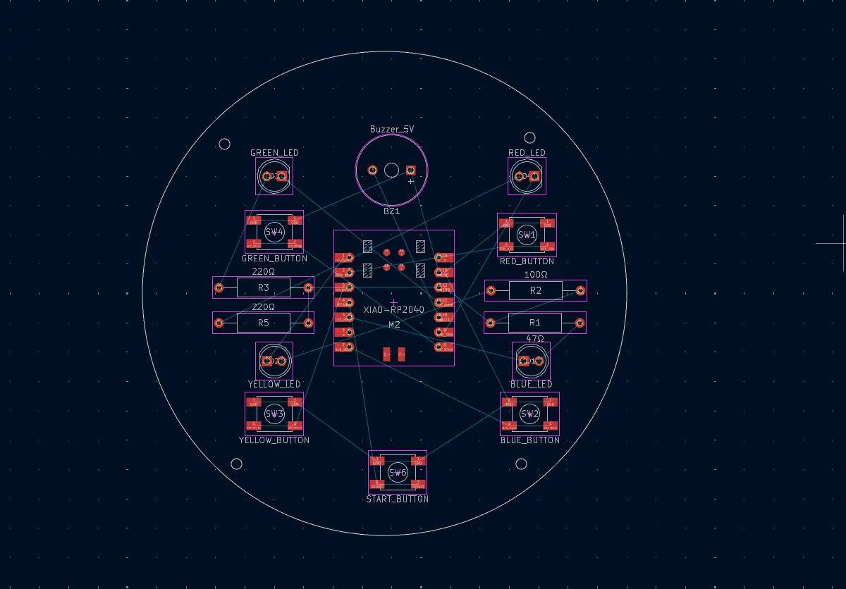
Now I was just a matter of trial and error to get the tracks just right. It took a little bit of pin relabeling, so that pins where near its target component. In the end, I came out with this layout:
The Copper Fill
A Copper Ground Fill is a layer of copper connected to ground that takes the extend of the empty space in your PCB. As we previously established, our machine will carve out everything but the tracks. In a big PCB, this can make printing times extremely big, as everything that is not a track is carved. Using a copper fill will make it so that the machine has to only carve the separation between the ground plane and the tracks, significantly reducing our printing time.
To add this to our design, we must first select our F. CU layer, and then press SHIT+CTRL+Z on our Keyboard. We must now trace the perimeter of our PCB. With rectangular / squared PCBs you can trace the actual perimeter. With every other shape, you can make a square around your shape. Once your square is fully connected, a window will appear. We must select our GND layer and add some custom parameters. For this first trial, I went with the following:
- Clearance = 0.4mm
- Minimum Width = 0.4mm
- Fill Type = Solid
- Remove Islands = Always
- Pad Connections = Solid
- Everything else as default
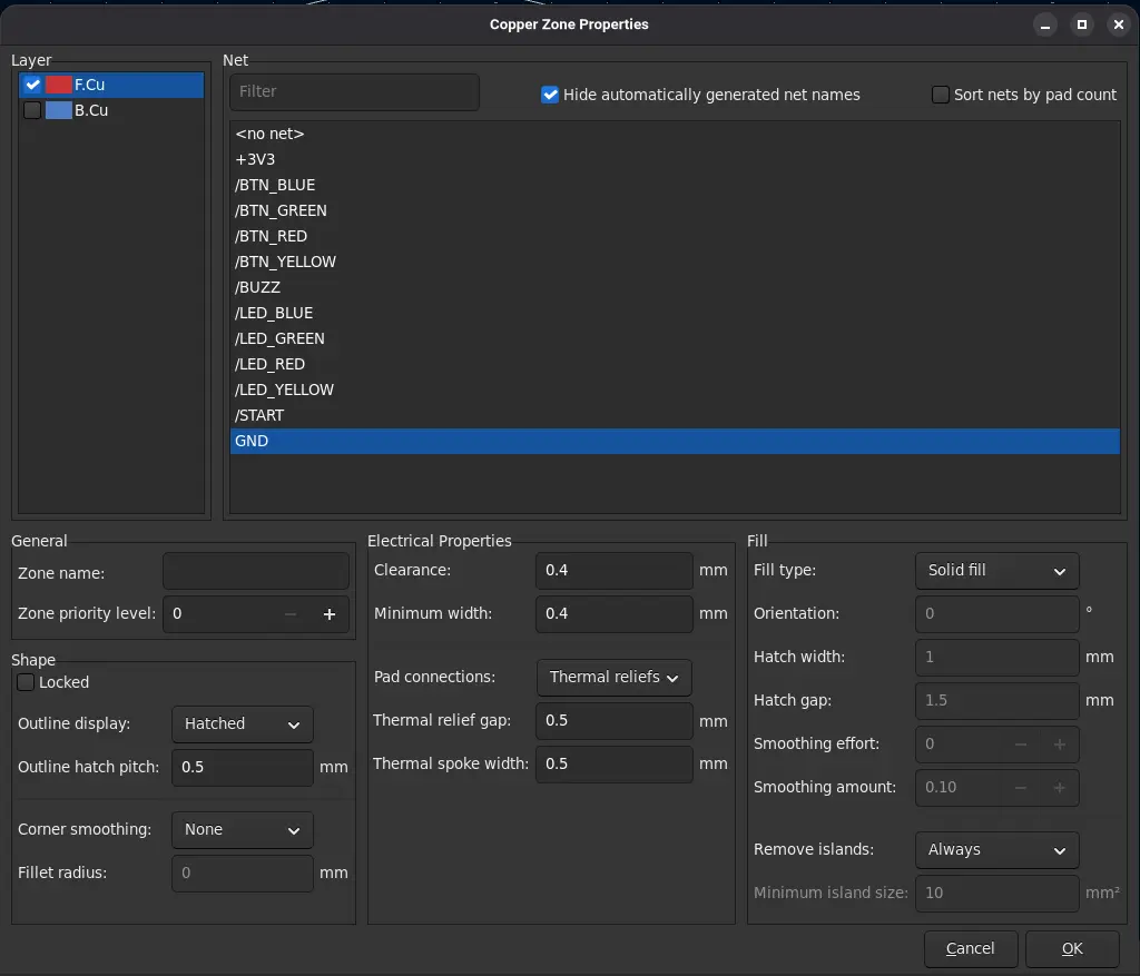
Now, click Ok. Then, click B on your keyboard. The copper fill will be added to your design.
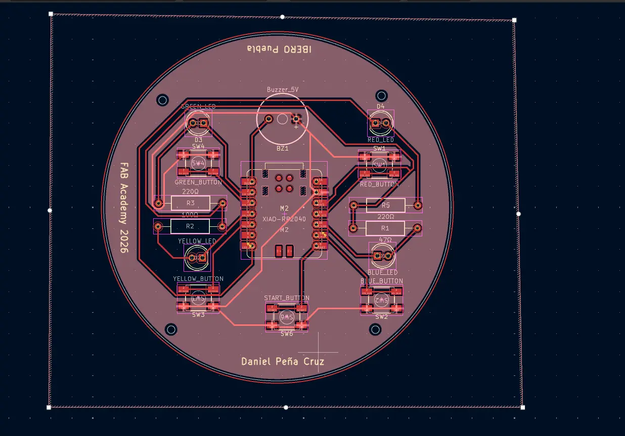
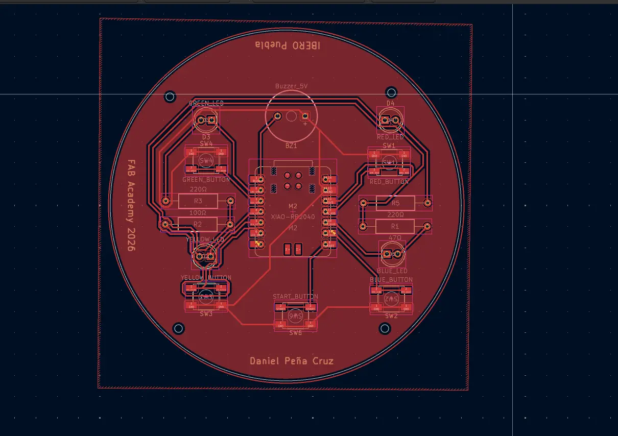
See those empty spaces? The Roland will still be carving those as they are not part of the copper fill. To solve this, we can optimize our tracks to be more compact, allowing the copper fill to better extend in the PCB. Remember, there are rules on how the copper fill can generate on your PCB. Once again, trial and error is an excellent approach. Once you have modified a track, click B once again and the copper fill will update. You can optimize your PCB as much as you wish.
A Couple Extra Modifications
After a first revision of my design, there a few modifications that still needed to be made before exporting to produce. This involved changing my components from Trough-Hole to SMD. The main difference between Trough-Hole and SMD is that Trough-hole requires perforations on your PCB and, usually, tracks underneath it for an easier solder. The more modern approach to components is Surface Mounted Device components, or SMD. Unlike Trough-Hole, SMD is soldered over the PCB.
Accessing Trough-Hole components is generally easier for the beginner user, as electronics stores are more likely to offer them. But in our Lab and university SMD components are widely available.
Changing our components in our PCB is as easy as changing the symbol on our schematic. We´ll be using 1206 model components for its size. We must change our resistors, LEDs and buttons. Our buzzer can stay as is.
Preparing for the Milling Machine
In order to prepare our GCODE for our Roland Milling Machine, we must first export our PCB design in either SVG or PNG format. We have a couple of ways to do that. The first one being exporting it directly from KiCAD with Files > Plot. Select SVG on the drop-down menu and click plot. You can also generate the Gerber file of your project, and use a Gerber to PNG converter like this one to generate a PNG if you desire.
Now we can generate our GCODE using modsproject page. In the menu on the up-left corner of the main screen, select the SRM-20 > Mill 2D PCB option (This might change with your milling machine availability).
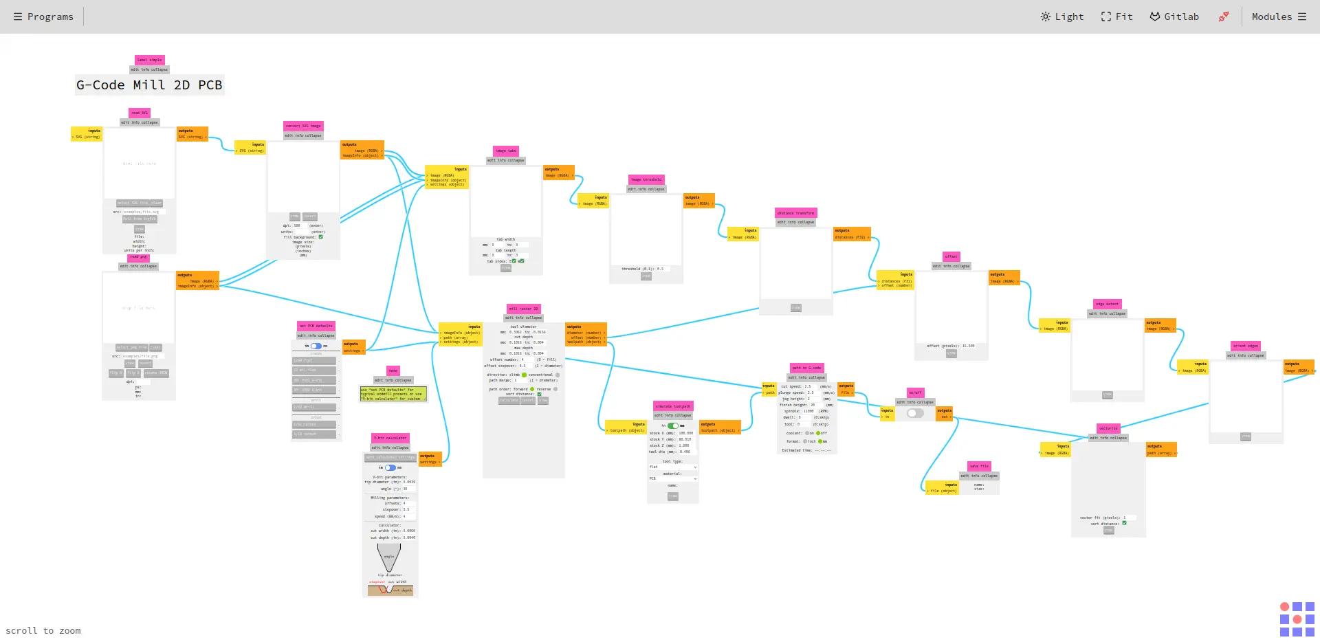
This screen with nodes will appear. Most of them we do not have to modify, they are just there to complete tasks for us in order to generate our GCODE. For starters, select the upload button for either SVG or PNG, and upload your image.
Note: Your initial image must be in black and white. Mods flips your image’s color, so everything white in your initial image will be milled away, and everything black will remain as copper.
You will see how your workspace will automatically modify itself. Now we must make some important adjustments before moving forward. Firstly, in the “set PCB defaults”, we have a selection of tools at our disposal. We will be using the 60 #501 V-bit option for our engraving, and the 1/32 drill for the edge cuts.
The “Mill raster 2D” will be modified. With this node we can better adjust our parameters for our specific drill bits. In my case, for the engraving tool, I made this modifications:
- Tool diameter: 0.4mm.
- Offset number: 1 (personal preference).
And for the edge cut tool, I just changed the tool diameter to 2mm, as we where working with a larger tool.
Modify the “Roland SRM-20 milling machine” node with these parameters:
- Speed: 2.
- x: 0.
- y: 0.
- z: 0.
And at last, switch on the previous node to the “Save file” node.
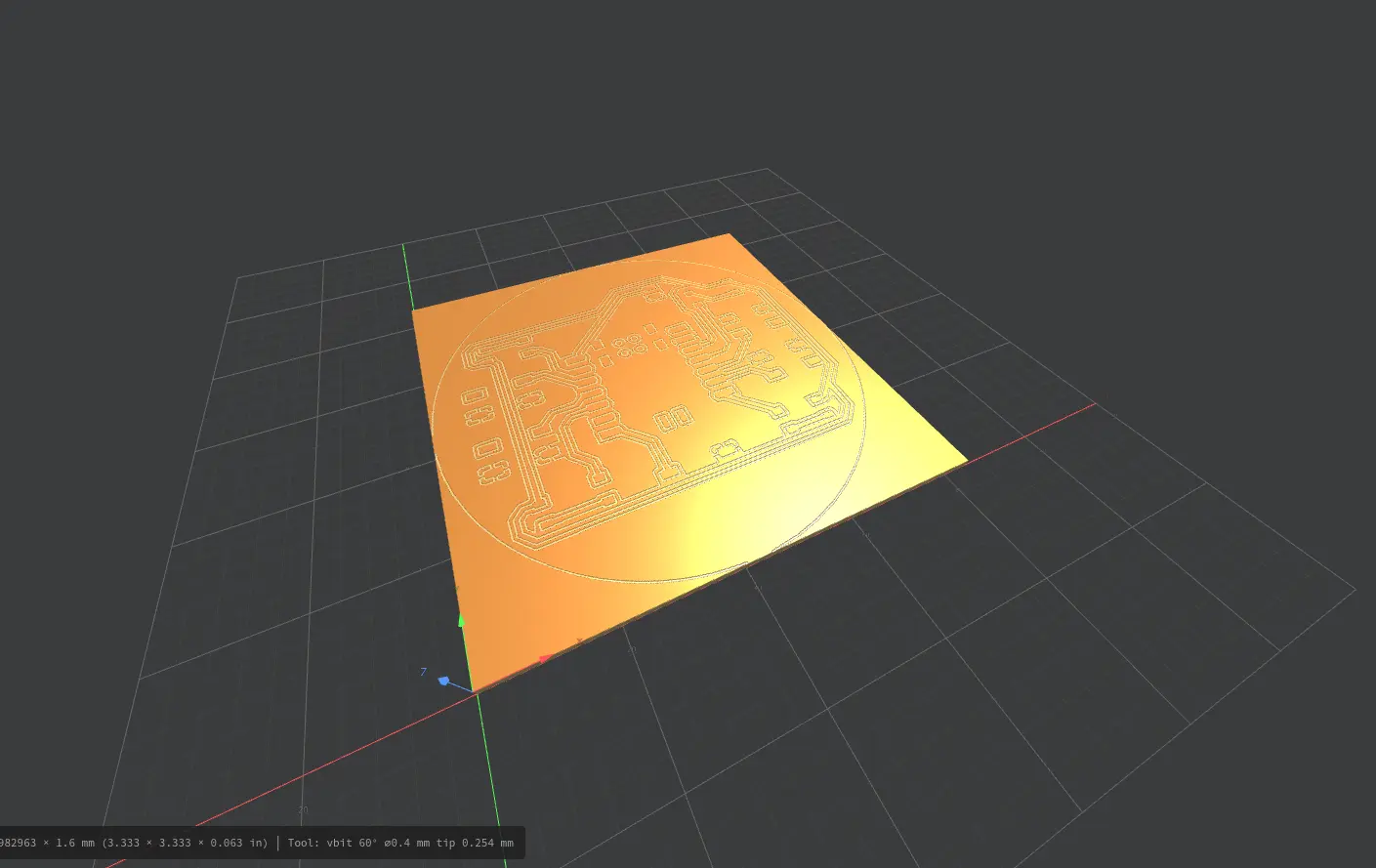
Now, return to the “mill raster 2D” node and hit Calculate. The program itself will generate your GCODE. Plus, a 3D render of your final product will appear on screen.
Now, with our GCODE ready, we can continue!
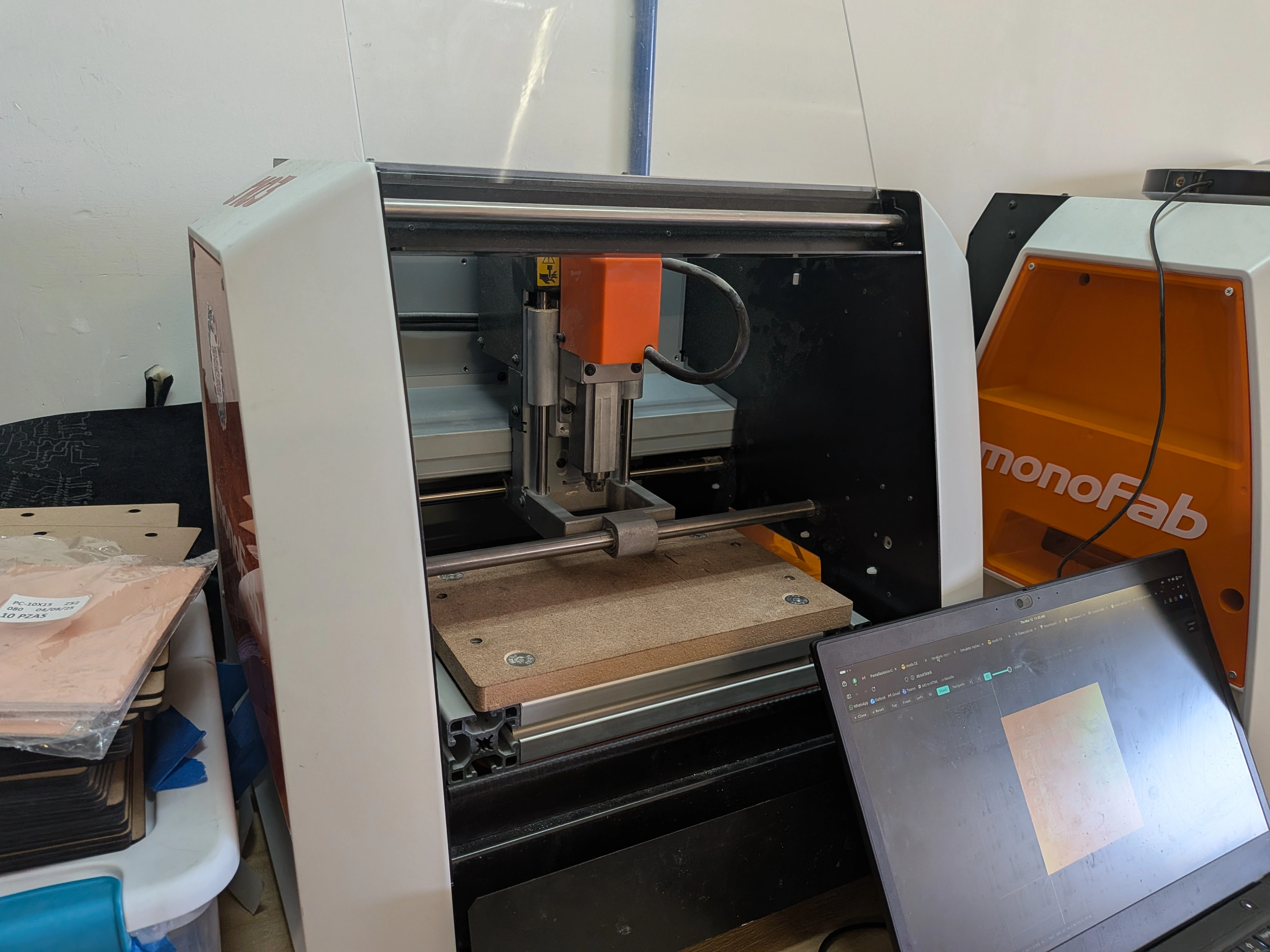
The Roland SRM-20
For this PCB, we will be using a Roland SRM-20 Milling Machine. For more information on how this machine operates and how to use it, check out or Lab‘s Group Assignment Page. From this assigment I learned the steps needed to engrave and cut a PCB in the Roland SRM-20 mini-mill, including setting up the copper plate, setting up the different engraving and cutting tools, and safety tips neede for its operation. This page also includes instructions on how to use the XTool F1 Ultra Laser Engraving Machine of our Lab. Sadly, I had no opportunity of using it in this week.
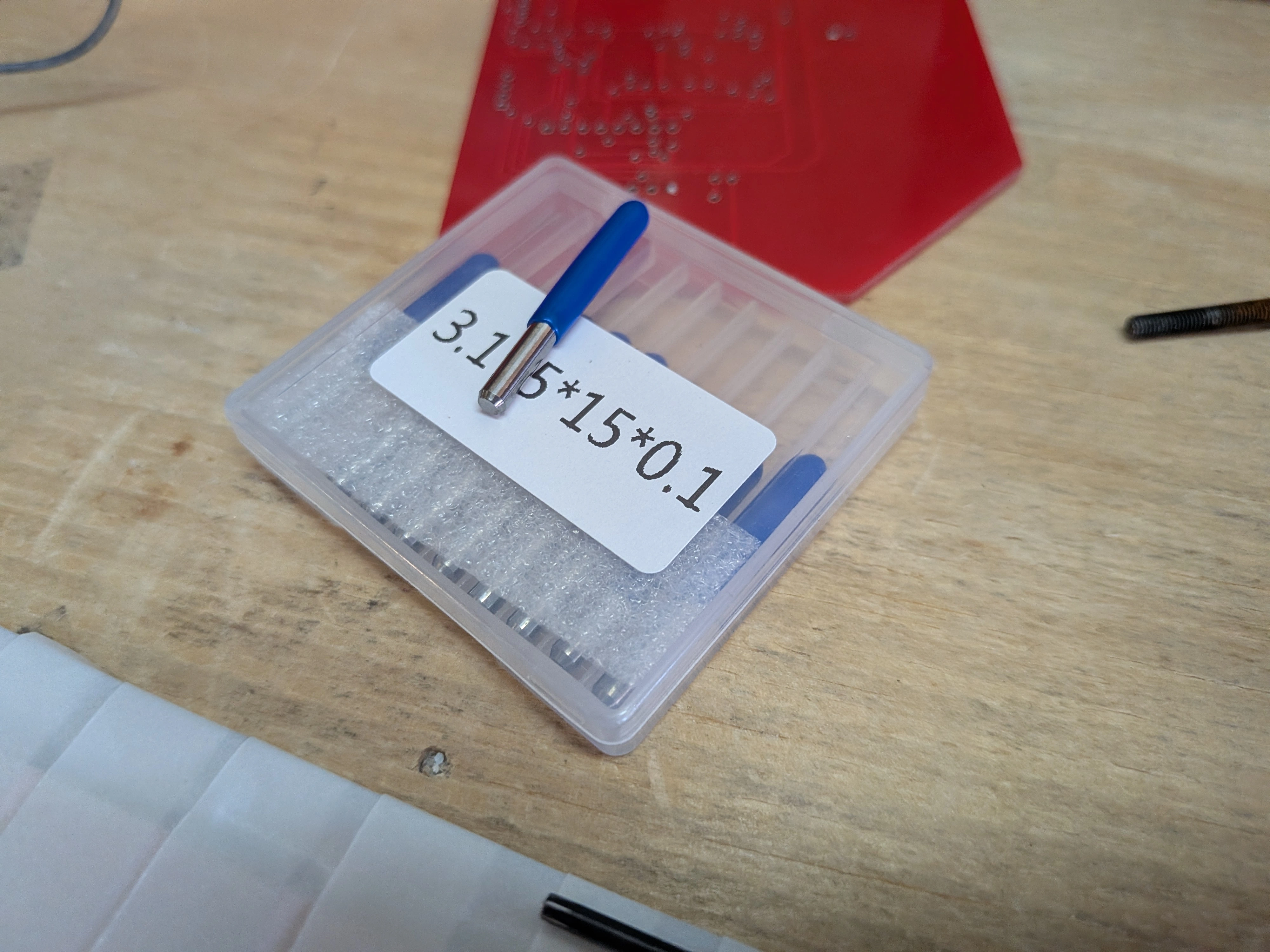
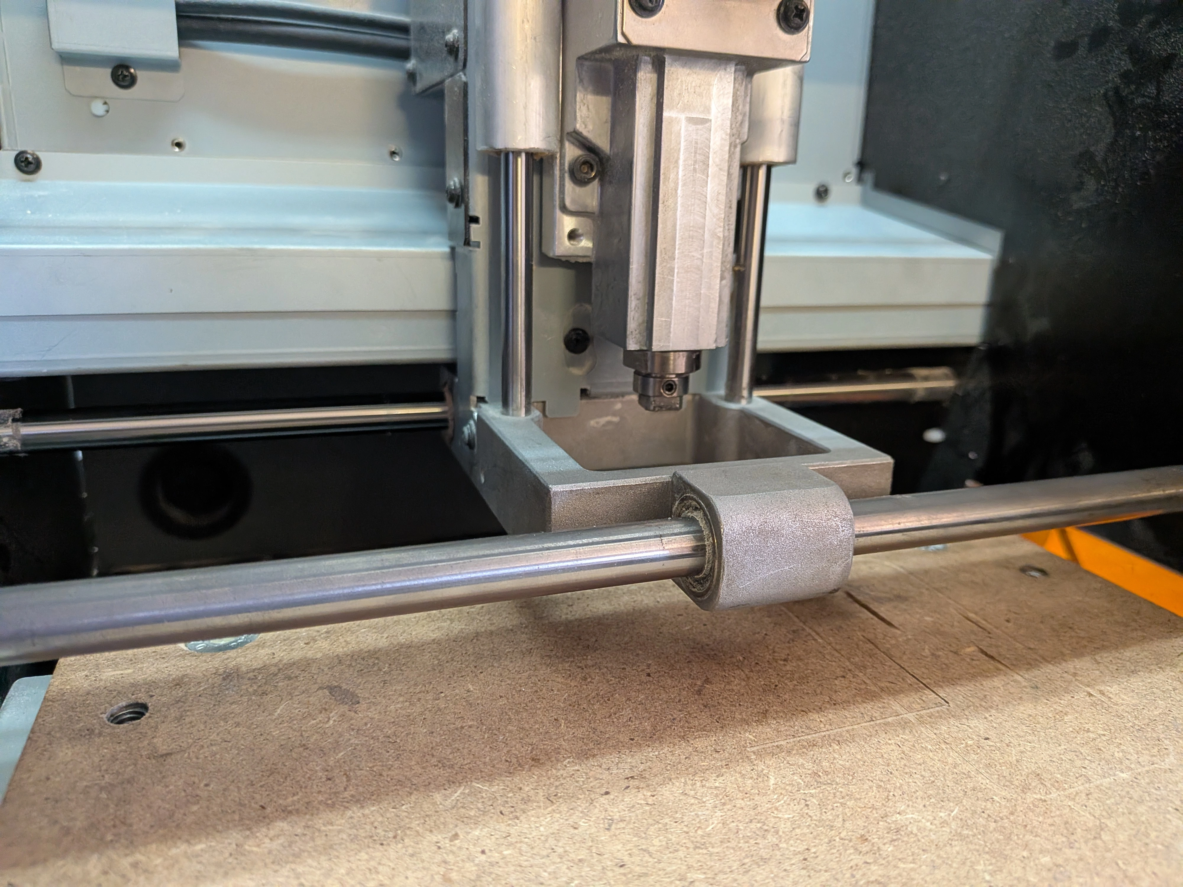
Step 1. Preparing the Milling Bit
To prepare the milling bit, we must first open the protective screen of the Roland.
Note: The Roland won‘t allow you to move the drill with the screen opened. Opening the protective screen while the Roland is operating will automatically stop the cutting process.
Now, grab your desired drill bit. Using an Allen key, secure the drill bit to the machine.
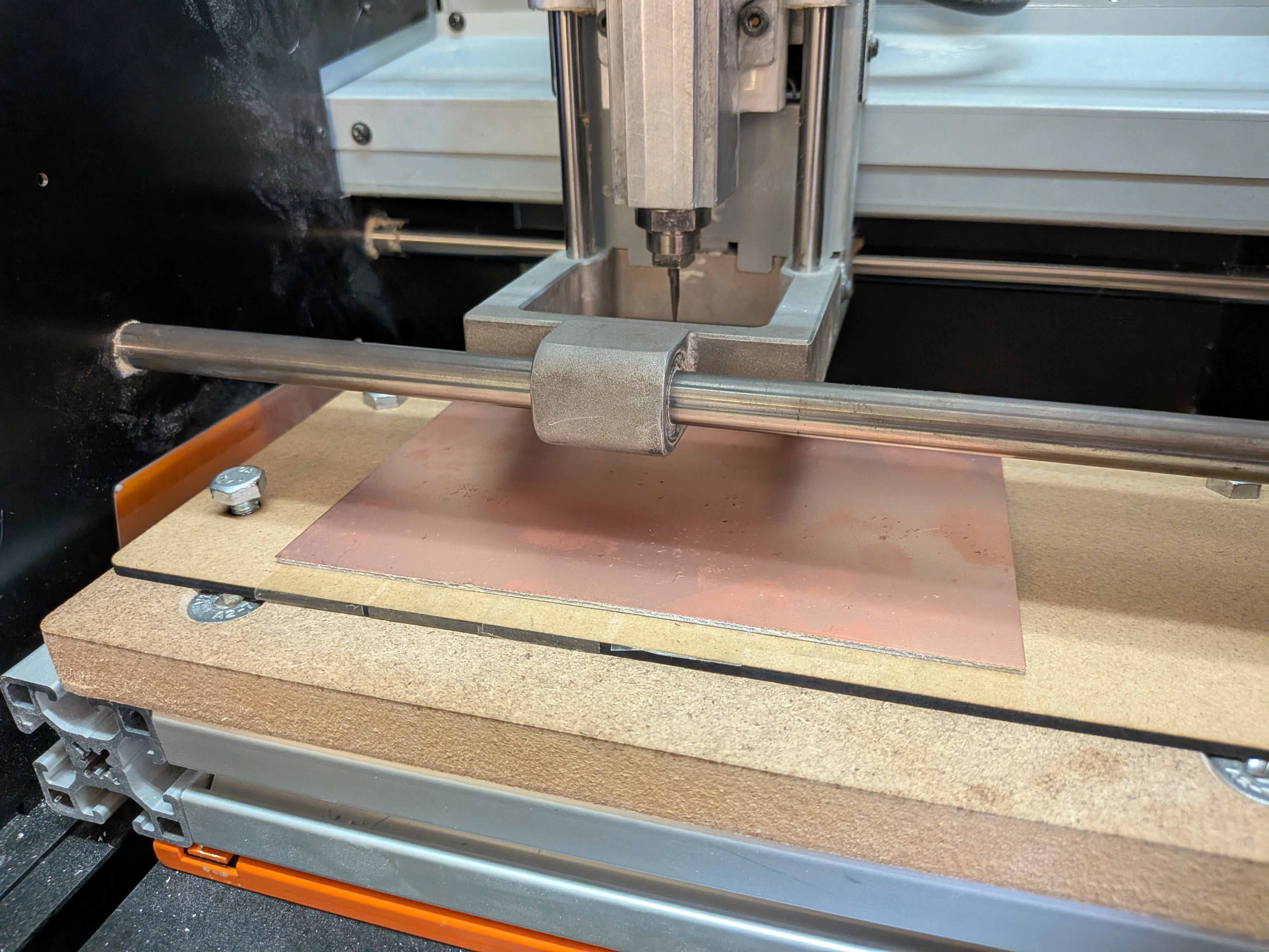
Step 2. Preparing the Copper Plate
We must also prepare our copper plate. To do this, we can simply paste the copper plate to an spare MDF plate called a “Sacrifice plate” with double-sided tape.
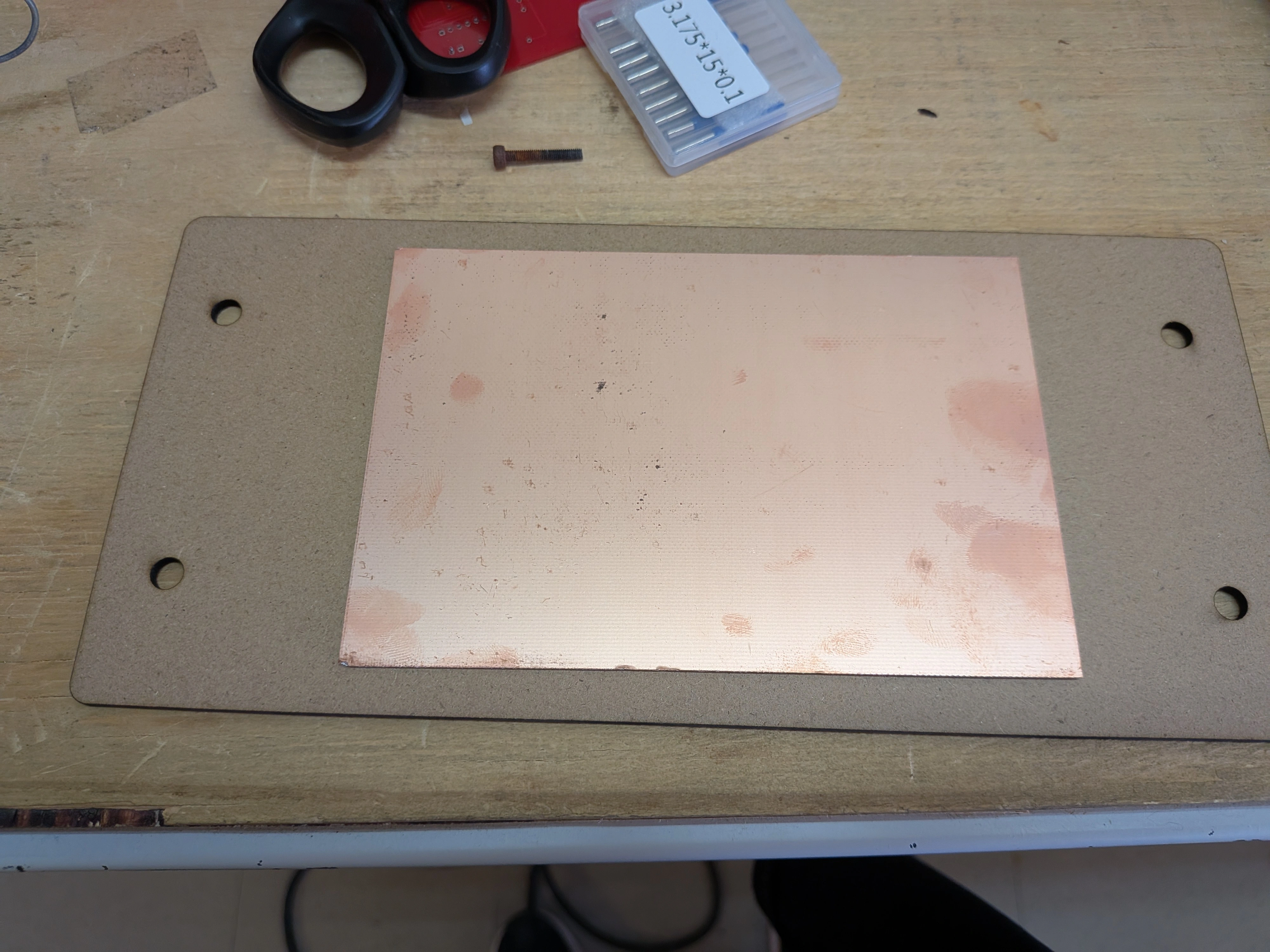
Now, we must secure the copper plate to the base of the moving base of the Roland with some screws.
Note: These screws must NOT be fixed tightly, as this can bend the plate and harm our final result. The screws must be fixed firmly but not as tight as possible.
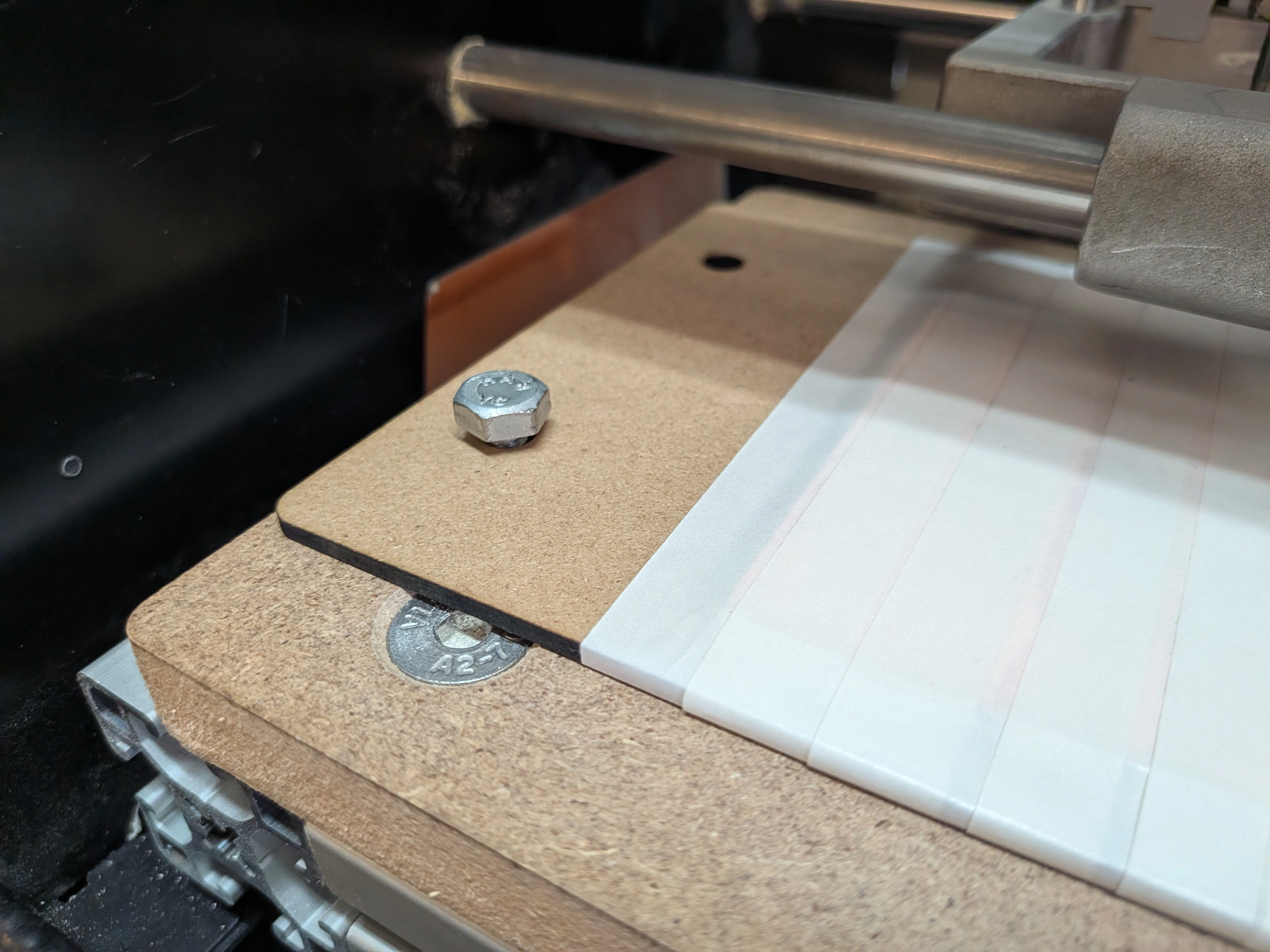
Note: Don‘t mind the tape placement on this photo. I misunderstood the instruction at first.
Step 3. Preparing our Computer
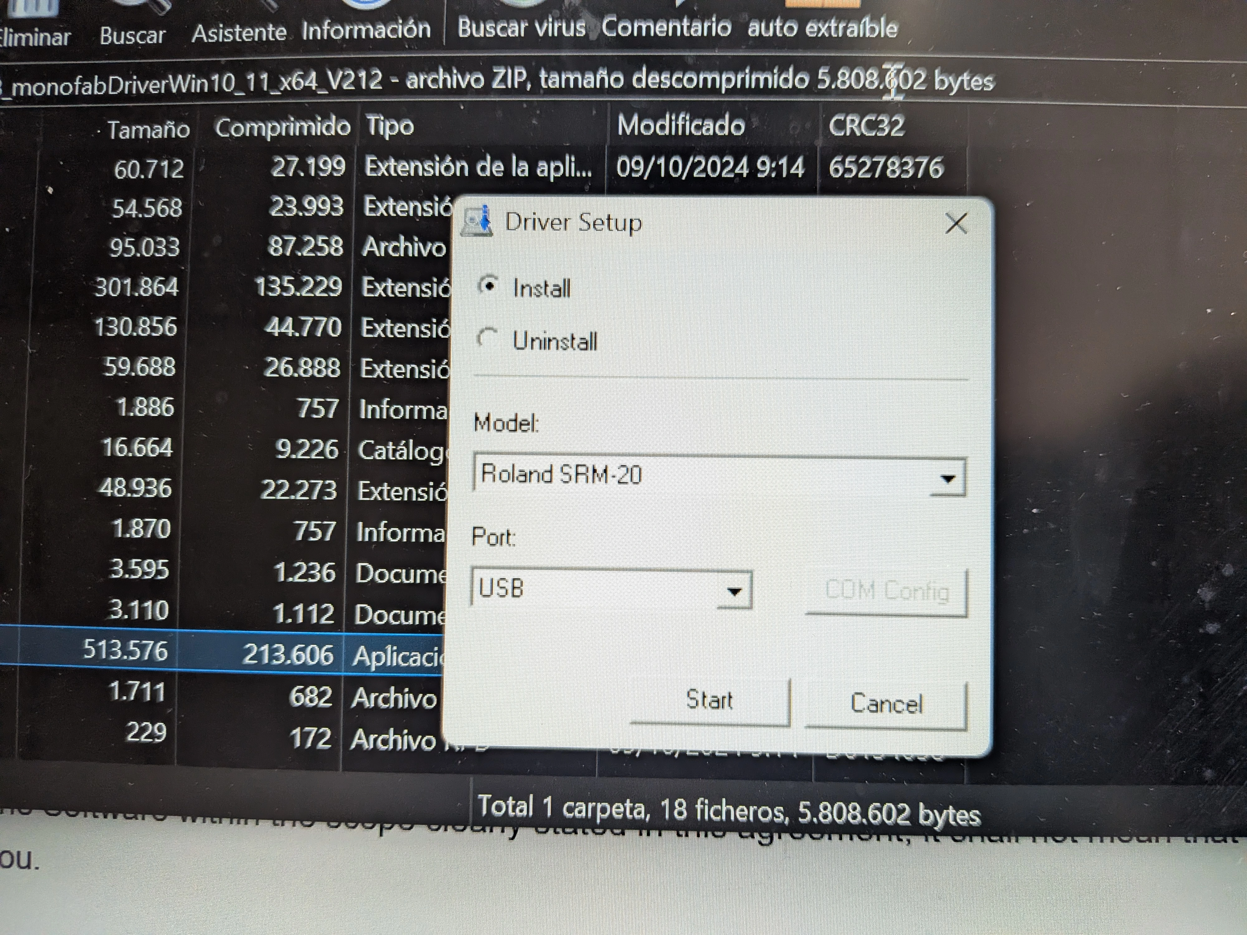
We need to get our computer ready to control our machine. To do this, we must download 2 essential software from DGShape‘s downloads page: The controller software and the machine‘s drivers for our computer. We must download “monoFab Driver” and “VPanel for SRM-20” and install them following their respective installation wizard‘s instructions.
Now we can connect our Roland to our computer with USB, and open VPanel:
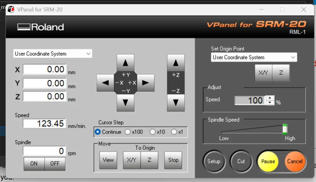
VPanel
With VPanel we can control our Roland‘s main functionalities. Using the various arrow keys we can move our drill on the X, Y and Z axis, we can set our origins, control our speed and pause/cancel our cuts. With our copper plate now fixed into the machine, we can set our XY and Z origins. The XY origins are a no-brainier, just make sure that your drill bit is set somewhere near the bottom-left corner of your copper plate.
Setting the Z Axis
Setting the Z axis can be quite a challenge. This is arguably the most important step of the process, as miscalculating the Z Axis by even 0.01 mm is enough to affect your final result. We can use our “Cursor Step” values to change the amount of movement of all our axis on every arrow press. The nearer your drill is to the copper plate, the slower your movement should be, as pressing the fragile drill bit to the copper plate can be enough to break it.
Note: A neat trick you can use is approximating the drill bit to the copper plate surface and dropping it by loosing it with the Allen key. The drill bit will now be laying on the plate‘s surface. Tighten up the drill bit again and now set your Z origin.
Also, make sure to calibrate your Z Axis on the center of your material (more on that later).
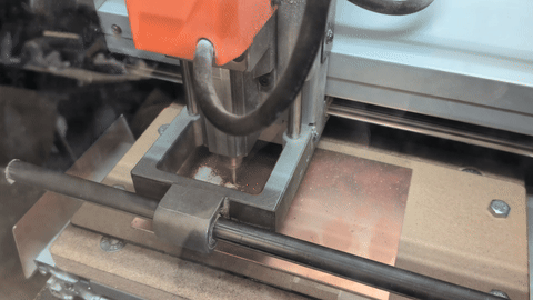
Now, with our Axis calibrated, we can finally proceed to mill our PCB!
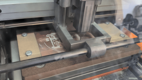
The First Attempt
My first trial with the Roland wasn’t as smooth as I had envisioned it. For starters, I have a lot of trouble setting the Z Axis on our machine (and apparently I wasn’t the only one). For whatever reason, setting the Z Axis on the center of the plate will make it so that the drill wouldn’t be correctly placed on the edges of the copper plate. Adjusting the Z Axis on the corners, however, will make it so that in the center the drill bit was pushed to much into the material.
With this issues unresolved, the actual cutting process had two distinct problems at the same time: there where areas of the PCB where barely any engraving was being made, and some where the drill pierced to much, breaking the drill bit in the process:
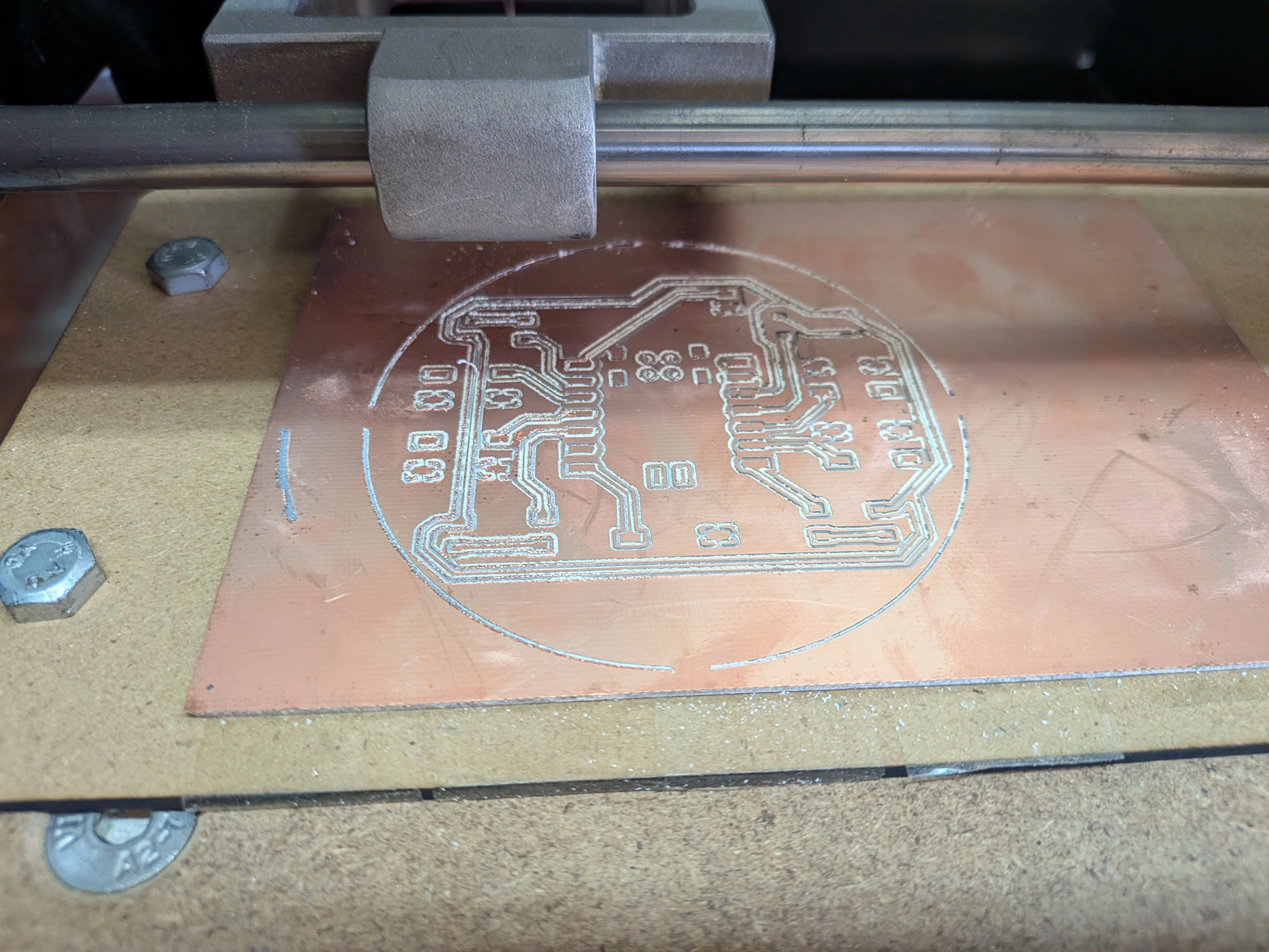
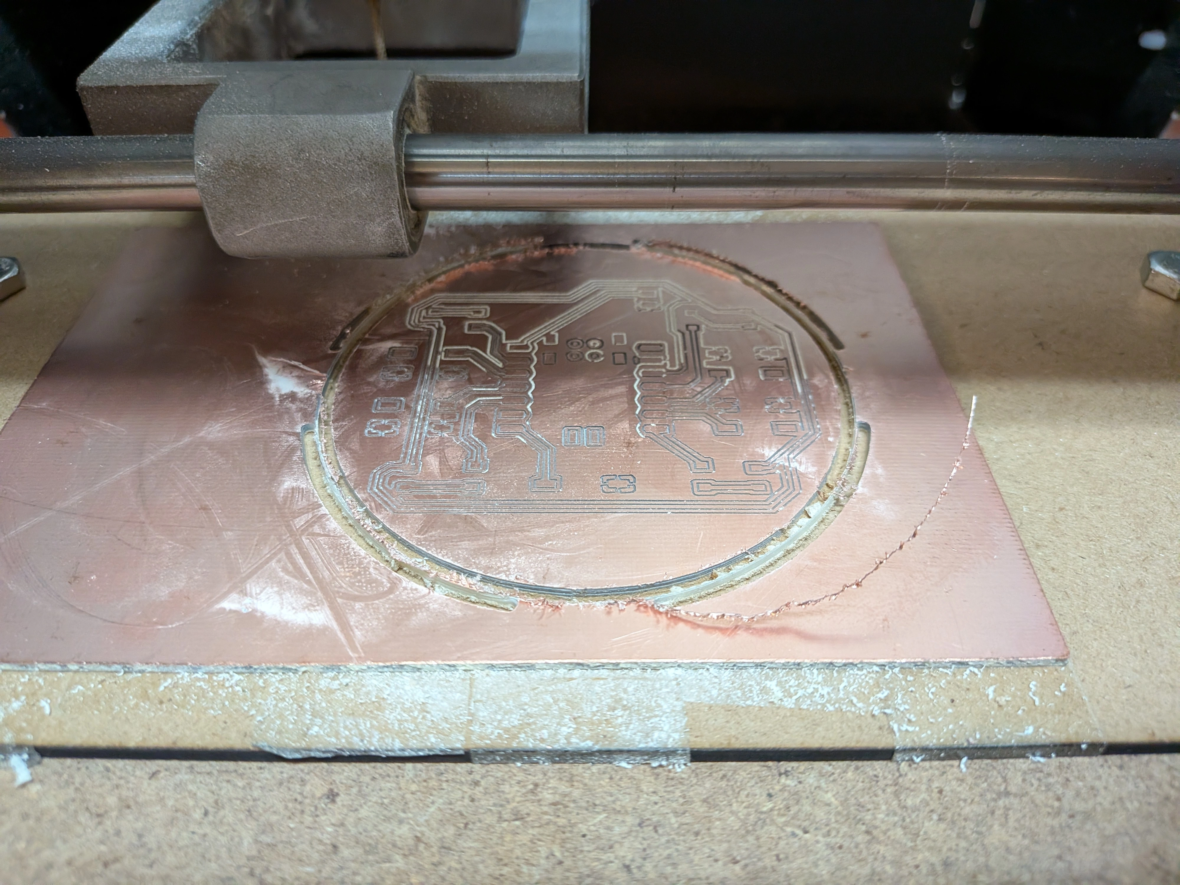
Still, after some trial and error, a PCB came out of the Roland:
Note: Once the PCB is milled, white dust will be present on its surface. This dust is highly toxic when breathed. Make sure to get rid of it with a vacuum before continuing.
And after cutting the edge, this was my very first PCB:
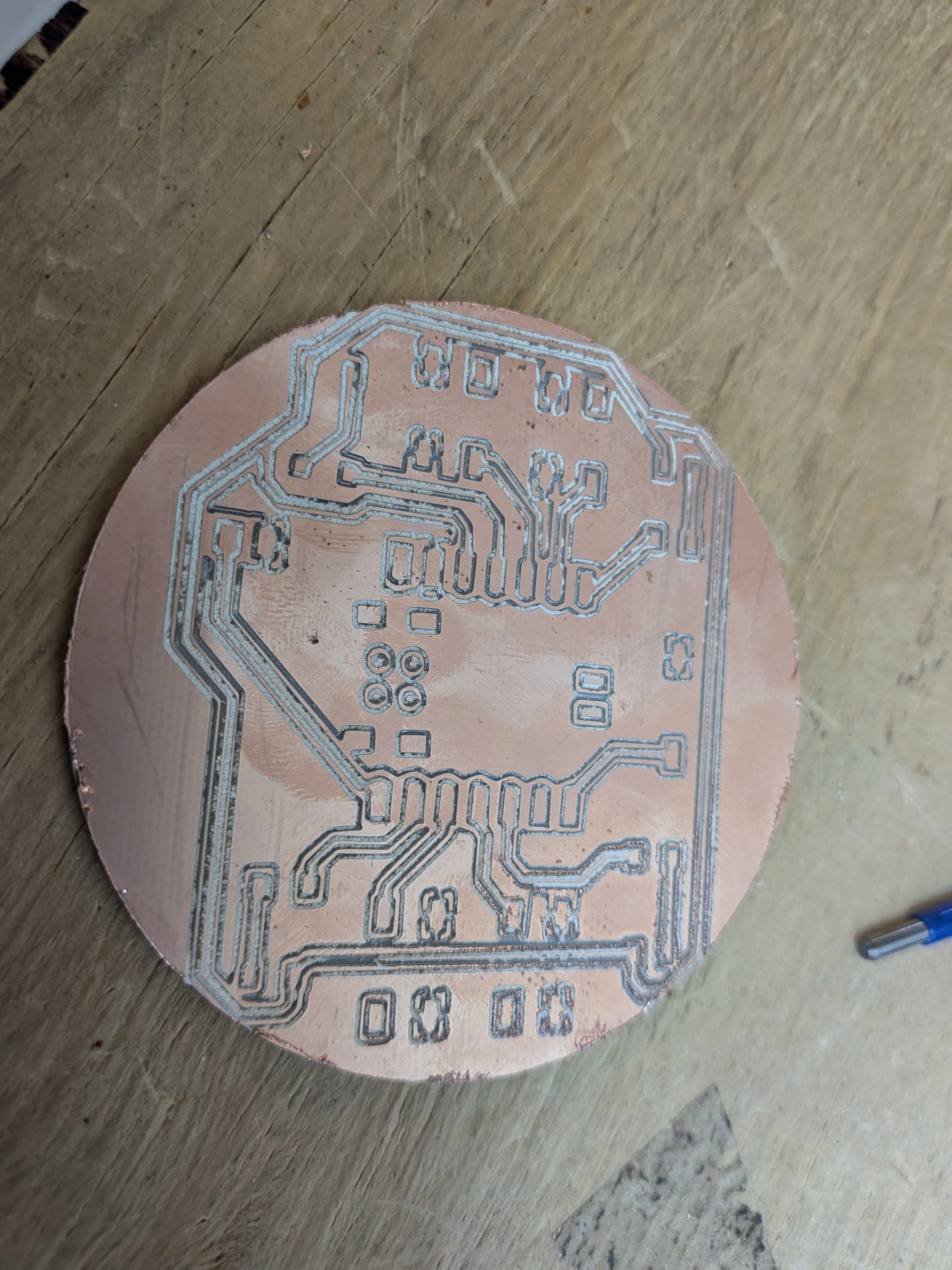
As you can see, there are a few things wrong with it. For starters, the cut itself is messy. This is because, at some point during (or even before) the milling process, the drill bit broke. Secondly, the drill engraved to deep in some places, breaking some of my main copper traces in the process. And third, the edge cut clipped some important traces as well. Overall, this first PCB wasn’t ready to be soldered in.
The Second Attempt
I attempted a second PCB with my new knowledge acquired. The main changes I made this time where:
- Made sure I raised the drill every time I moved it and before starting the cut, to prevent the drill bit from breaking.
- Changed the XY origin more to the center of the copper plate, trying to combat that weird difference between the edge and center‘s Z height.
- Used the “dropping the drill bit” method to calibrate the Z Axis origin.
Now, with this modifications, our second attempt went way better than the previous one.
This time, our traces where perfectly defined and our PCB ready for the soldering process!
Soldering our Components
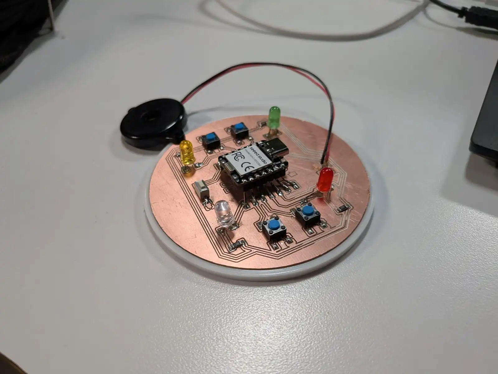
As much as I would have love it to end on a high note, something went wrong in some step of the PCB production. We were working with SMD components, 1206 sized to be precise. Plus, a Xiao RP2040 that we had to solder to the PCB. No problem, as I already have experience and practice soldering components to PCBs with soldering iron and heat gun.
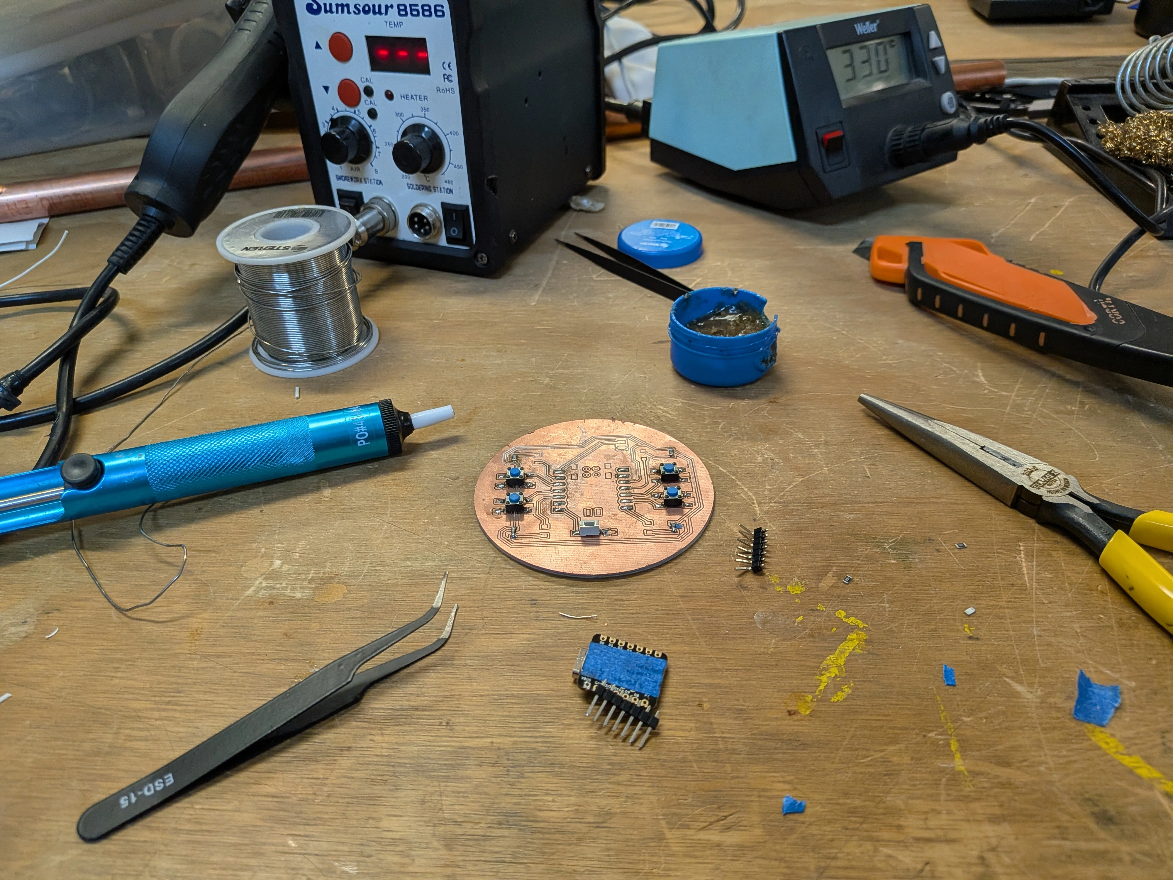
The problem came with the soldering pads positions, more specifically their size. You see, when designing the PCB in KiCAD, I selected the FAB’s libraries footprints for each component, mainly the 1206 resistors and the Xiao RP2040. This should have make it so that the sizes on the final PCB matched the actual real life component size. But for whatever reason, mine where bigger, as I they where scaled up.
My leading theory is that, when converting the Gerber file to PNG, the page scaled the image to fit content, up-scaling the component‘s footprints. Some components had no problem being connected, like the buttons. But for the resistors and the Xiao RP2040 itself, the task was almost imposible.
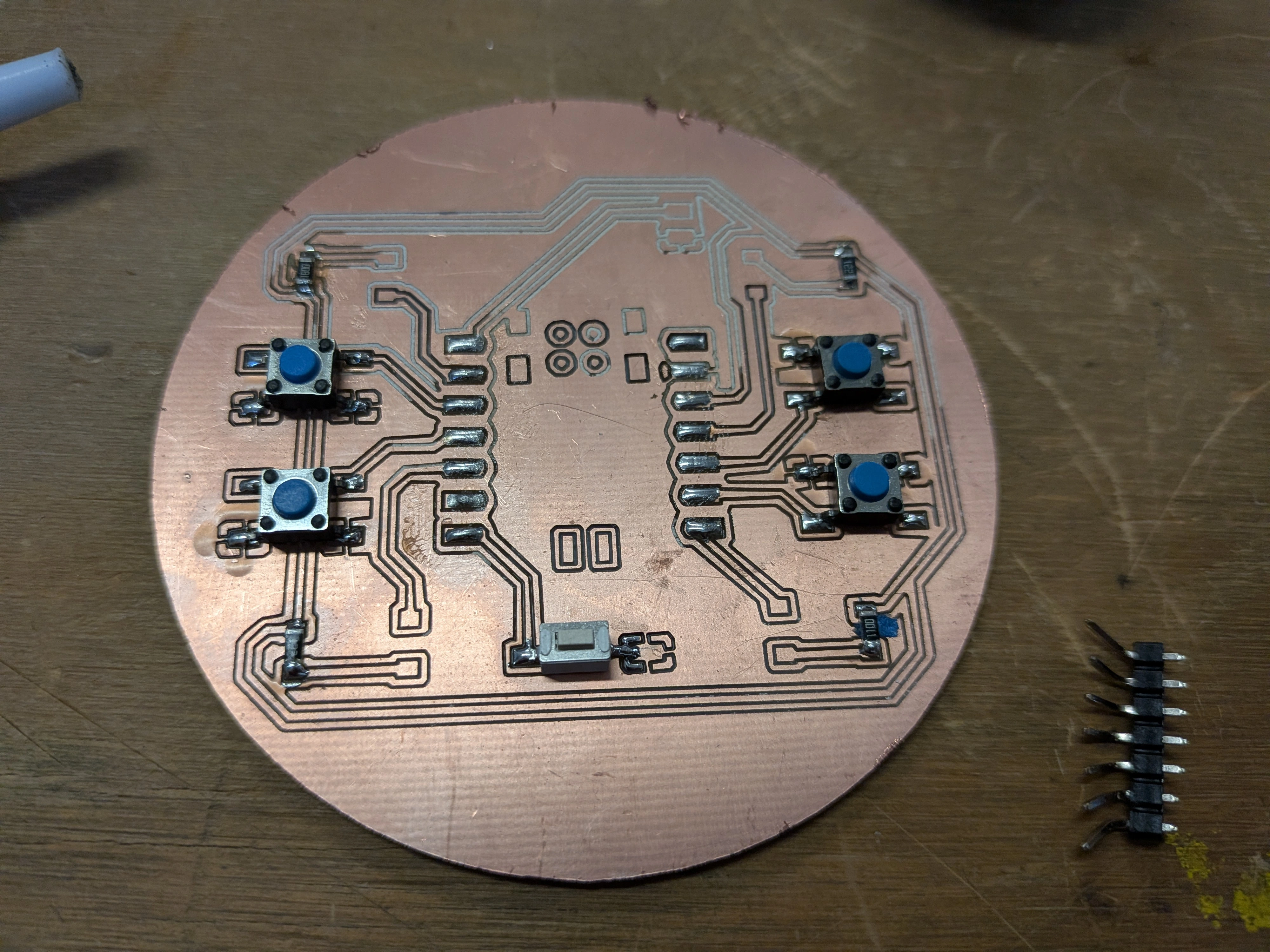
I was able to somewhat work around the resistors, using some masking tape on their bottom to prevent contact with the ground plane. The Xiao, however, was trickier as the pads and pins where impossible to align. I tried fixing it by bending and soldering some Pins to create a bridge between the components:
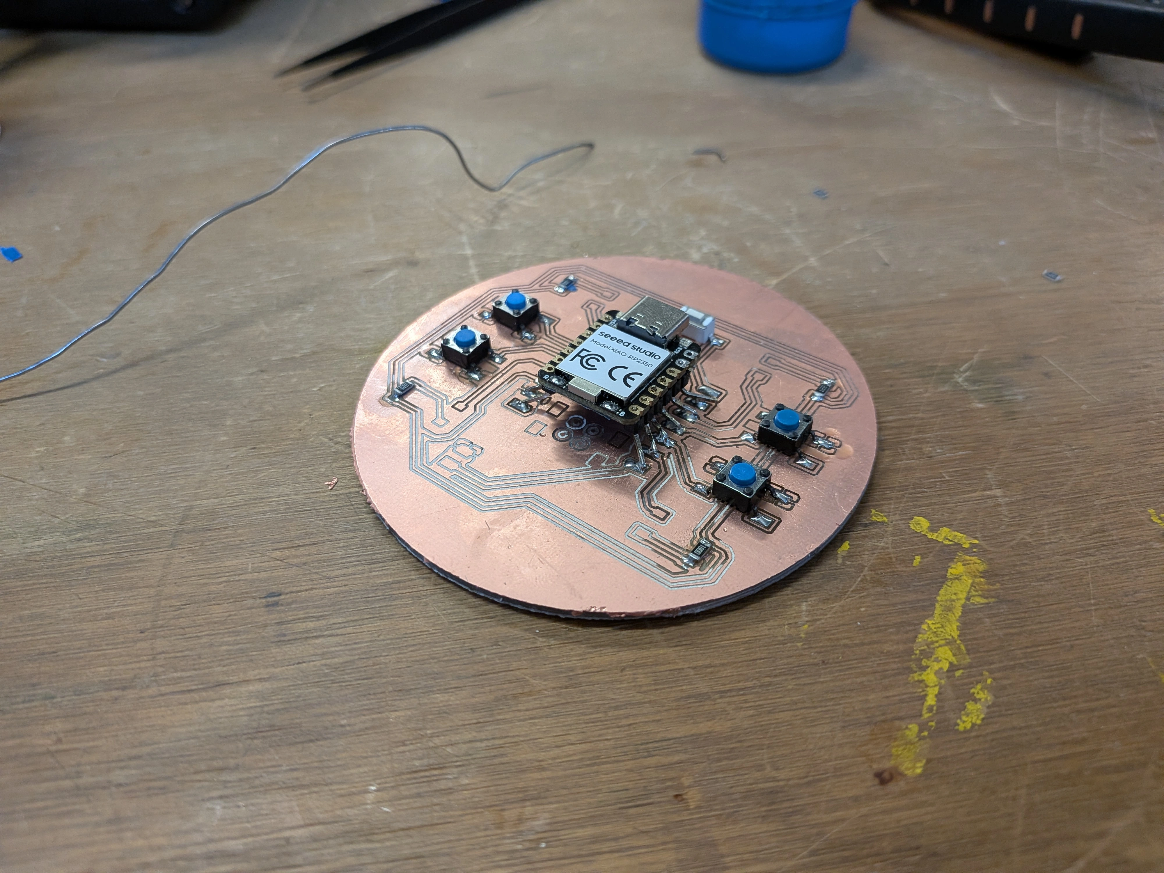
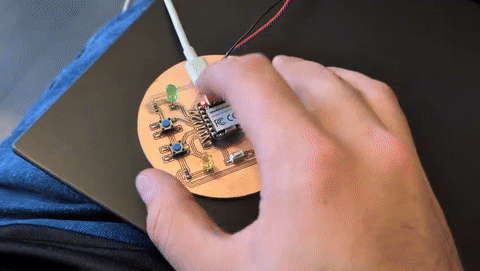
Soldering the LEDs was also a hard task to achieve. I ended up deciding to use regular Trough-hole LEDs to facilitate its soldering. Plus, I think regular LEDs give it a more playful look. With all connected, it was time to load my Script into the Xiao. This was an easy task, as the code was already made in Wokwi in week 6. I only needed to modify the pin number for each component and some small tweaks.
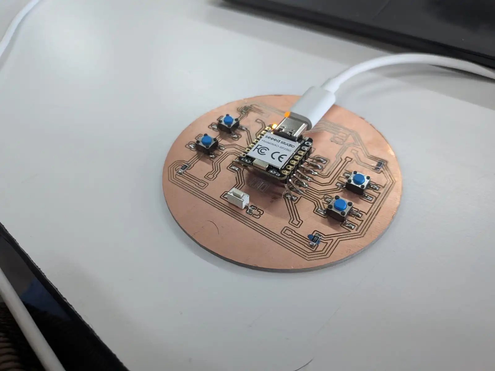
At first, only the red LED turned on. I had no idea as to why it was behaving like that. Then I figured it out: The Xiao wasn’t making full contact with the pins. I ended up soldering the pins to the Xiao, which almost solved the issue. Every LED worked fine, except for the Green LED. It turns out the resistor wasn’t properly soldered. I de-soldered it and soldered again. This time, everything worked out as expected, and I had my Simon game ready to play!
Extra Credit: PCB Case
On week 6 I also designed a parametric PCB casing in OpenSCAD. The PCB had some size modifications, so I only needed to change one variable and the whole model was ready. I the imported it into Ultimaker Cura, prepared the file for printing and send it. The print took 1 hour, and in the end, resulted in a perfectly fit bottom case for the PCB. I miscalculated the size of the case borders, but regardless it functions as a perfect protection for the down side of the PCB.