Electronics Design
Electronics Design refers to every step involved in the creation of electrical circuits. This electrical circuits can then be physically made with a bread board and electrical components. For most, this is already a pretty big step forward. Bringing your very first circuit to life, even something as simple as powering an LED, it´s enough to make you fall in love with electronics.
For us FAB Academy students, though, building en electrical circuit in a bread board is just the beginning. Our project will require their own custom-made electrical circuits that sadly cannot stay in a bread board. We need to design our custom Printed Circuit Board (or PCB for short). A PCB helps us compact our electrical circuit, removing the need of external wires. With a PCB, every wire is replaced with a copper route that connects our soldered components.
Designing you own PCB is essential to ensure your project has everything it needs to work correctly. It is a process that requires some basic electronics knowledge. If you understand how electrical circuits work, and how the most used electrical components work (resistors, capacitors, LEDs, buttons, etc.), you are good to go.
For more information on the process of designing electronics, check out our Lab’s group assignment. From this assignemt I learned the basic electronics measurement, like voltage and amperage, and its measuring tools like the multimeter and Oscilloscope. Having a basic understanding on how electronics work is essential for correctly designing a PCB full of electronical components and a constant power supply. Plus, knowing how to use this tools is a desired skill for debugging our PCBs and understanding what is going on through them.
Electronics design is divided into 3 main steps:
- The idea.
- The Schematic.
- The PCB design.
The “idea” is straight forward: you must first know what you want to do in order to make it. Making a prototype on paper or even a bread board can make you visualize your PCB and be ready to work on it.
The Idea
We´ll be using a Xiao RP2040 micro-controller for the brain of our PCB. It is important to note that using a micro-controller is not mandatory for PCB design, it is just a way of making our lives easier, and allow us to do stuff that would be harder to make with bare bones electronics.
My idea is to create a Simon Game. For those who don´t know it, Simon is a memory game, where different colors are shown in a continuous patter that randomly grows with every round.

This is an excellent first PCB project, a it only requieres a few components to work, keeping our PCB simple and allowing us to work with the few pin availability of the RP2040.
Prototyping in Wokwi
To make the prototype, I booted up Wokwi. Wokwi doesn´t offer the RP2040 itself, but this micro-controller is based on the Raspberry Pi Pico platform, which is available. I chose to work with MicroPython for a fast prototyping and to better understand the logic of the game.
Essentially, to code a Simon Game, You need an Array (or list). This Array will save the sequence of colors. Every round, a random color from the color list (red, blue, green, yellow) will be added to the list. Now, for each element on the list, will need to read if the current input matches the color of the sequence. If it does, we continue until the round is finished. If not, we lose.
For those who understand flowcharts, here is the flowchart of the game logic:
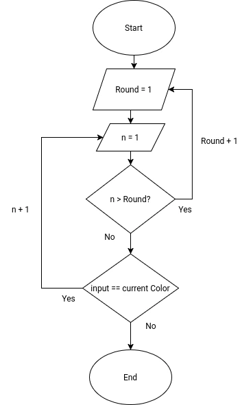
Programming this in python is pretty straight forward, and with our knowledge on embedded programming from week 4, we where able to not only code the came, but also make the electrical prototype for it.
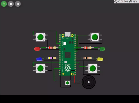
I won´t be placing the code here, as it is quite long. But you can find it in the files section of the page. The python code will be compiled to the RP2040. And this image of the build itself will be our blueprint for our next steps.
KiCAD
For the next two steps, we´ll be using a program called KiCAD. KiCAD is a mix of different software that help you throughout every step of a PCB design. To start using KiCAD, you can download it from KiCAD´s official website.
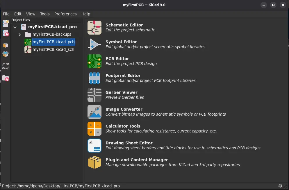
Opening KiCAD for the very first time, you´ll see this menu:
The amount of options might seem overwhelming, but essentially we´ll be using three:
- The Schematic Editor.
- The PCB Editor.
- The Plugin and Content Manager.
First, go to File > New Project to create a new project. A file will be created. This file will contain your project file, your schematic file and your PCB file.
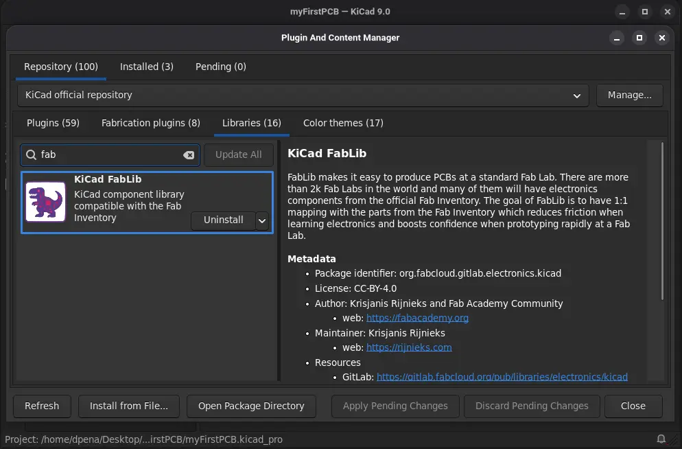
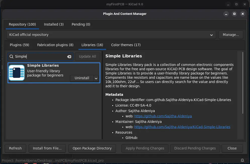
Before we start, click on “Plugin and Content Manager”. A window will appear. Click on “Libraries” and search for “FAB” in the search bar. A library will appear. Click install and then Apply Pending Changes. This will install a FAB made library of components:
Another library I personally recommend is the “Simple Libraries”. This will contain a couple of essential electronics componentes for us to use:
Now we can close this tab and begin our PCB design journey with our second step: the Schematic.
Schematic Design
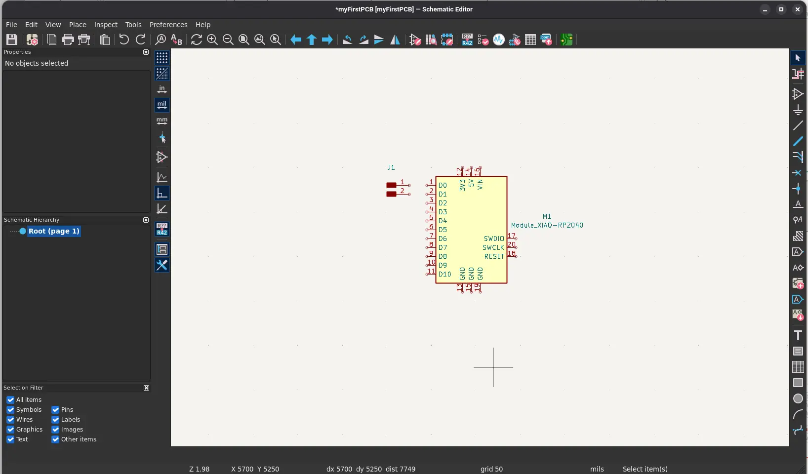
Opening the Schematic Editor for the first time, you´ll see a blank workspace. Working in KiCAD is really straight forward. With the right side menu (or with keyboard shortcuts) you can place and connect electrical symbols.
Fun fact: in my free time I like to learn about Electronics repairing, specially laptop repairing. One of the most useful skills I´ve learnt is Schematics reading. So this might be my first time building a PCB, but the previous knowledge on schematics reading made me feel like home.
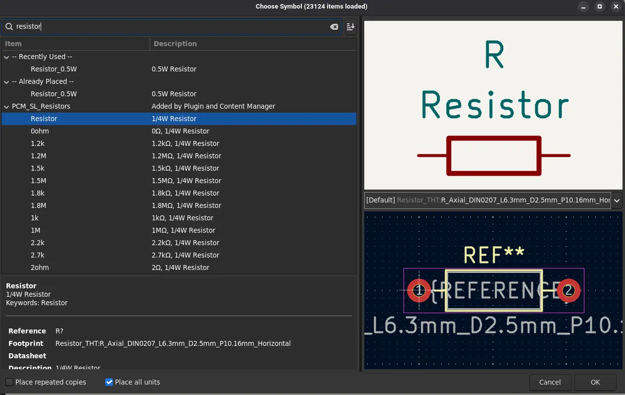
To place a new componente, you can type A in your key board. A new window will appear. You can use the search bar to search for your desired component and select it. Two images will appear on the right: The first images (the one on top) will be the symbol, or the image that will appear in the workspace of the schematic view. We can connect the symbol to other components. The second image (the one on the bottom) is the footprint, or the actual space the component will have on the PCB.
Note: Be careful! Not every component has a footprint file. If your desired component has no bottom image, this means it won´t be translated when we switch to the PCB editor in the future.
If by any chance your component is not in the components list, you can search for it online by typing your component followed by “___ KiCAD symbol and footprint”.
Now you can place your component. Now, we´ll look at the most common tools you´ll be using:
- Typing B will let you create connections between components.
- Typing L will let you create labels, that declare “wireless” connections between components. This one is helpful for segmenting your schematic into main circuits and joining them without an actual connection.
- Typing Q will let you mark a connection end as “not used”.
With this tools we can follow our Wokwi prototype and create our own connections:
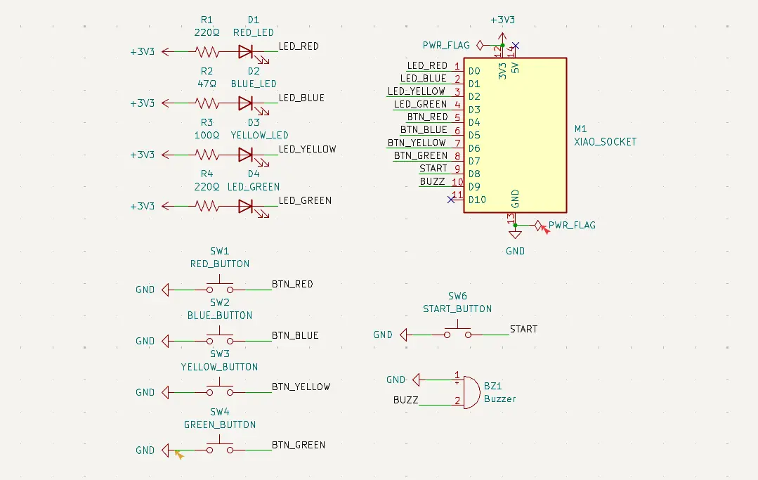
Here´s whats going on.
- The big block is the Xiao RP2040 socket, where the actual micro-controller will be placed. From here, every GPIO connection is sent.
- The first array of lines are the LEDs. Each LED is connected to the 3V3 line of the Xiao. They also have their mandatory resistor with their value changed according to every LED color.
- The second array of lines are the buttons for each LED. Each button is connected to both ground and their LED line.
- There is an start button connected to the START line.
- There is a buzzer connected to the BUZZ line.
Electrical Rules Check
On the top menu there is a “Check list” icon called the Electrical Rules Check (or ERC). This tool will take a look at your schematic and tell you it there are any electrical problems with it. ERC is a MUST before completing your schematics and go to the PCB design, as this will ensure your PCB won´t have any problems moving forward.
For example, my first schematic had a couple of problems involving the 3V3 and GND line. The Xiao socket knows there will be power going out those pins. Marking those pins with a simple “+3v3” and “GND” pin confuses the simulation, triggering an error. To solve this, I added a “PWR_FLAG” besides the 3V3 and GND pins, letting the simulation know “There will come power out of here”.
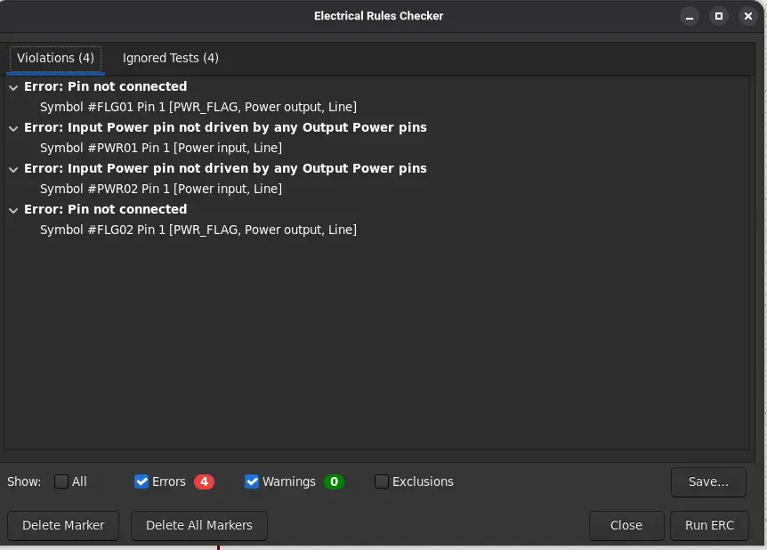
If the ERC returns no errors and your schematic is completed, your are now ready for the third and final step: PCB Design.
PCB Design
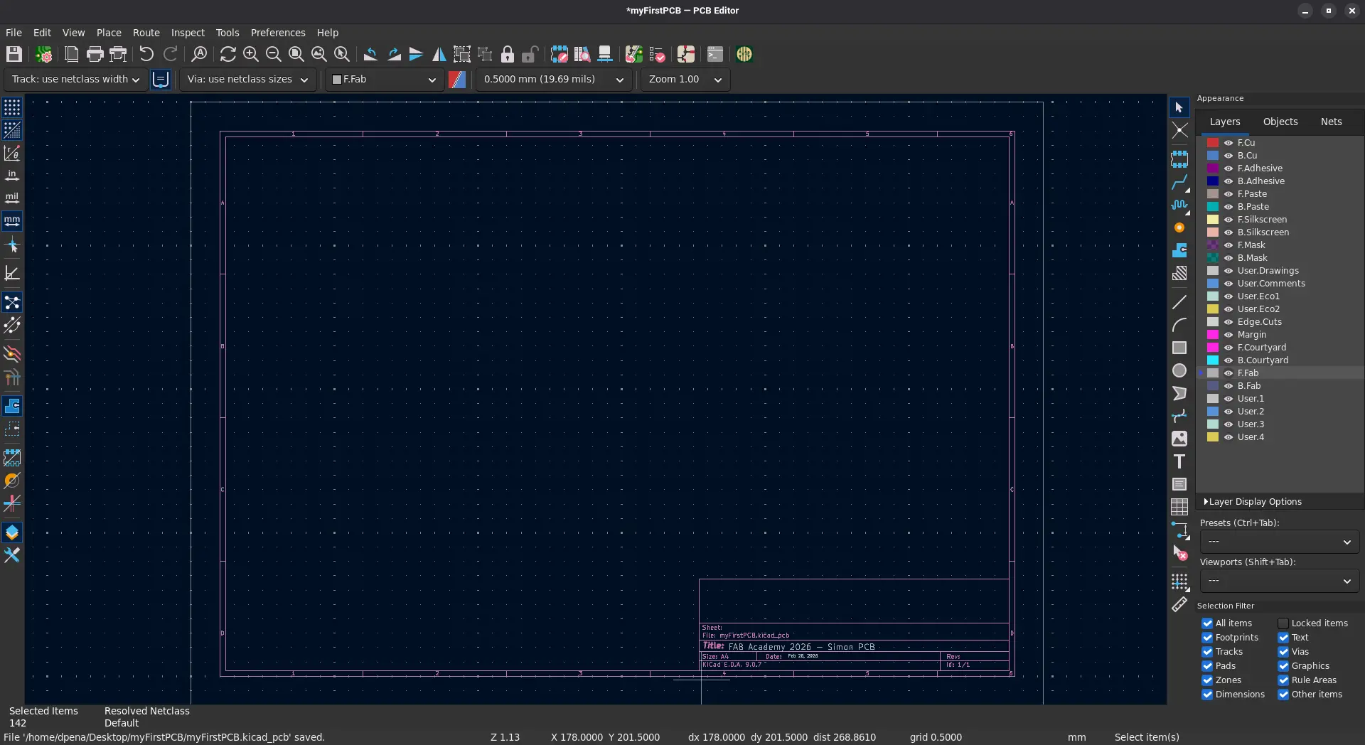
We can now change our view to the PCB editor. Opening the workspace for the first time, we will not see our components yet:
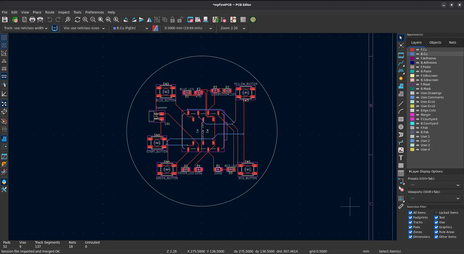
To import our components, look for the “Update PCB from Schematic” button in the top menu bar (the one with a half-schematic and half-pcb icon), or simply type F8 in your keyboard.
A clump of components will appear.
Component Arrangement
Your first step is arranging your components correctly. There is no “correct” way of doing it, its just trial and error. There are dim blue lights connecting your components. If your schematic was well done, this lines represent components that connect to each other. Arrange your components in a way that makes those lines overlap the least.
You can also determine the exact size and shape of your PCB. On your right side bar there is a list of all the layers of your PCB. Click on the “Edge.Cut” layer. Now, using the drawing tools on the toolbar, draw your PCB´s shape.
Routing
It is now time to connect your components.
There is a KiCAD plug-in called “Auto-route”. This plugin helps creating component connections automatically. I highly DISCOURAGE you using this tool. For starters, when I tried using it, the PCB was configured to use more than one copper layer. Spoiler for the Electronics Production week: We will only have a single layer with the PCB creation methods available in most of our Labs.
Plus, there is no better way of learning than doing it yourself. Even with a couple of components, routing can be a challenge. It requires a lot of component movement and trial and error, but it´s worth the time investment. After a lot of trial and error, my PCB was routed.
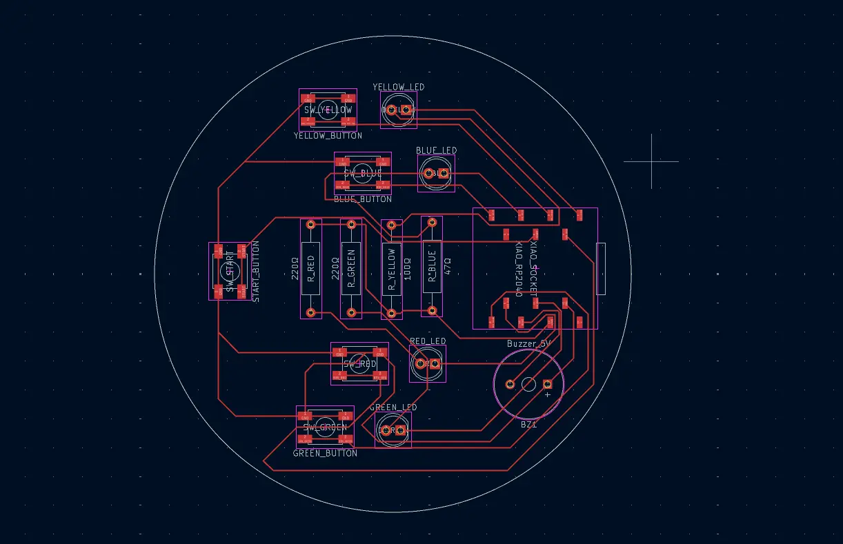
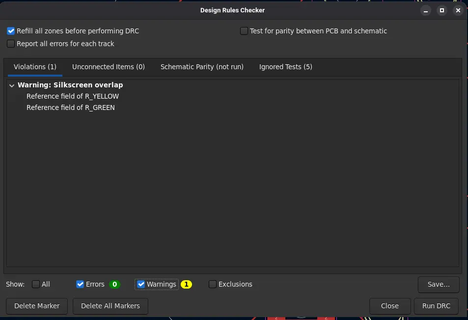
Design Rule Check
Similarly with the ERC for schematics, the Design Rule Check (or DRC) is the last step in our PCB design journey. Running the DRC will let you know it there are any mistakes present in your PCB. Luckily for me, I had no design Errors, just a couple of warning of overlapping text. Does this mean my design is perfect? No. It just means that, electrically speaking, our PCB will work. There are a lot of advanced electrical rules that apply to more advanced PCB, and most of those won´t appear on the DRC. But for our first PCB, having no Errors is enough.
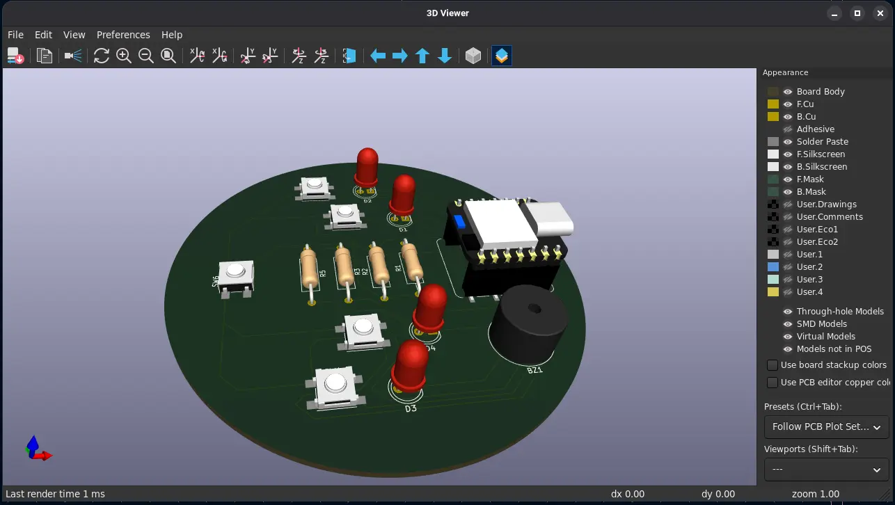
The 3D View
Now, as a reward for our hard work designing and constructing our schematic and PCB design, we can take a look at how our PCB will look once in our hands. To do this, go to the “3D view” button in the top menu (the one with a capacitor icon).
Now, your PCB will be rendered in a 3D viewer, where you can move around and appreciate your PCB on detail.
Extra Step: Designing a Casing
This is an optional step to do, but designing a case for your PCB is a perfect way to not only practice your 3D design skills, but also keep your work more protected (plus, its an extra credit). In the PCB Edit view, KiCAD already offers you some important information about your PCBs shape. For example, my PCB is round, so I´m given the radius of my shape. This might be enough to start designing a case. But for more advanced cases or for weirder shapes, this won´t cut it.
Luckily for us, KiCAD also allows us to export our PCB in .stl format. This means that we can import our PCB to any CAD software we desire in order to have a better look at the piece whilst designing, and making better adjustments.
To export our PCB 3D model, go to File > Export > STEP/GELP/…/…/STL. A window will appear. Select STL in the dropdown menu, leave everything else as is.
A crude STL model will be created. Now let´s design our case. To do this, I´ll be using OpenSCAD again. We´ll create a new project folder, where our .scad file will be but also our .stl file, more on that later.
Using our PCB radius data from KiCAD, we can begin creating a case:
difference() {
              linear_extrude(height = caseHeight)
              circle(r = pcbRadius + caseBorder);

              translate([0, 0, 2])
              linear_extrude(height = caseHeight)
              circle(r = pcbRadius);

              translate([0, 0, 1])
              linear_extrude(height = 1)
              text(text = "FAB Academy", size=5, halign="center");

              translate([0, -8, 1])
              linear_extrude(height = 1)
              text(text = "2026", size=5, halign="center");

              translate([0, -16, 1])
              linear_extrude(height = 1)
              text(text = "Daniel Peña Cruz", size=5, halign="center");
          }
This code creates our base case, with a dip for the PCB. Bonus points for the embedded text on it´s bottom.
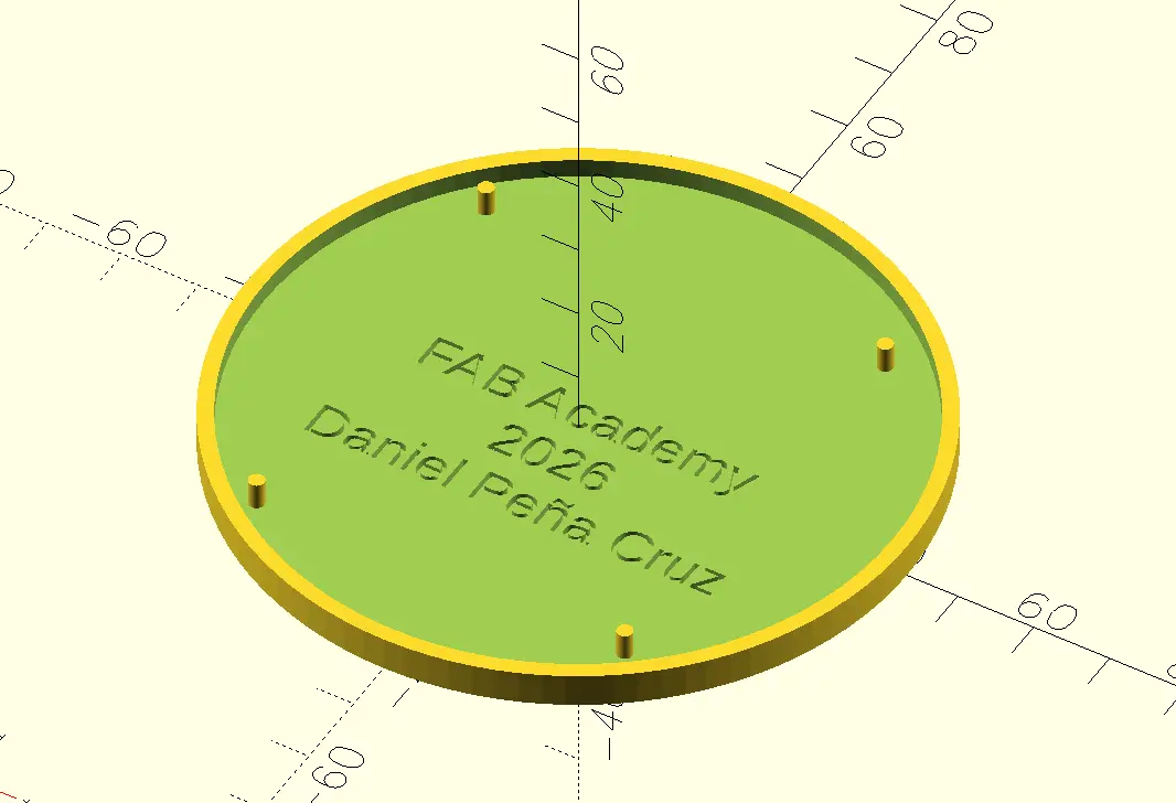
We also added those pins to better lock the PCB with the casing. To add those wholes in the PCB, simply add circles in the Edge.Cut layer of your PCB design.
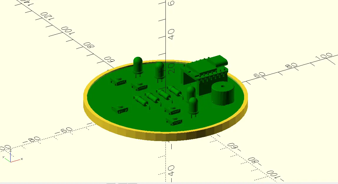
Now, we can use the import() function to import our .stl model. If the .stl file is located in the same folder as the .scad file, you can import it like so: import(myFirstPCB.stl). The PCB will instantly appear on your screen. If the file is not in your project folder, you can place the exact route to it.
And that´s it! On week 8 (Electronics Production) we´ll be printing this casing as well.
Next Steps
For now, our PCB will be staying in file format. However, on week 8, we´ll be bringing it to life. The knowledge acquired during this week will also be needed further down the line for our Final Project. You can check my Final Project´s page for the Electronics Design section on the Development tab. There will be more on my project´s PCB journey.