
Week 08 | Electronics Production
Group Assignment
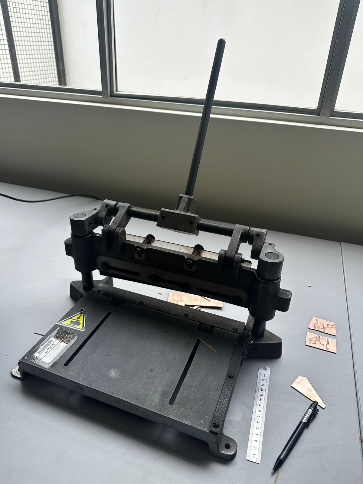
This week's group assignment consisted of characterizing the PCB fabrication process using the equipment available in the laboratory. The objective was to understand the workflow for producing printed circuit boards, including milling the copper traces with a CNC machine, drilling the component holes with a bench drill, and cutting the board using a manual shear cutter. The activity was carried out in the Electronic Laboratory of the Pontificia Universidad Católica del Perú (PUCP).
The complete documentation of the group work can be found in the following page:
Group assignment documentation
Individual Assignment — Week 08
During this week the complete process of fabricating, assembling, and testing a printed circuit board (PCB) was carried out in the electronic laboratory of the Universidad Católica del Perú - PUCP. The objective was to understand the full digital fabrication workflow for electronics, from the design files to the final functional board.
1. Preparing the PCB Design in KiCad
The first step consisted of preparing the PCB design previously created in KiCad. Before exporting the file, the PCB was reviewed considering the limitations of the CNC milling process. Since the board would be fabricated using a subtractive method, the design parameters had to ensure that the milling tool could physically reproduce the geometry.
The trace width was set to 0.4 mm, with a clearance of 0.4 mm between traces. These values were defined based on the limitations of the CNC milling process, ensuring that enough material could be removed between traces to achieve proper electrical isolation.
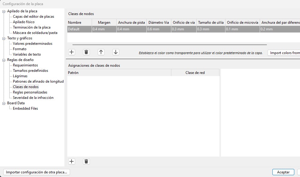
Design rules configuration in KiCad showing trace width and clearance values used for CNC milling.
In addition to the trace width, several design parameters were defined in KiCad to ensure compatibility with the CNC milling process. The clearance between traces was set to 0.4 mm. Although vias were not used in this single-sided design, default values were configured to maintain consistency in the rule set.
The PCB was designed as a single-sided board, avoiding vias and minimizing the complexity of the routing. In this design, the ground was not routed as a separate trace because the copper surface of the board was used as a ground plane.
After completing the PCB layout in KiCad, the design was exported as an SVG file. This vector format allows the circuit traces to be directly processed and converted into toolpaths.
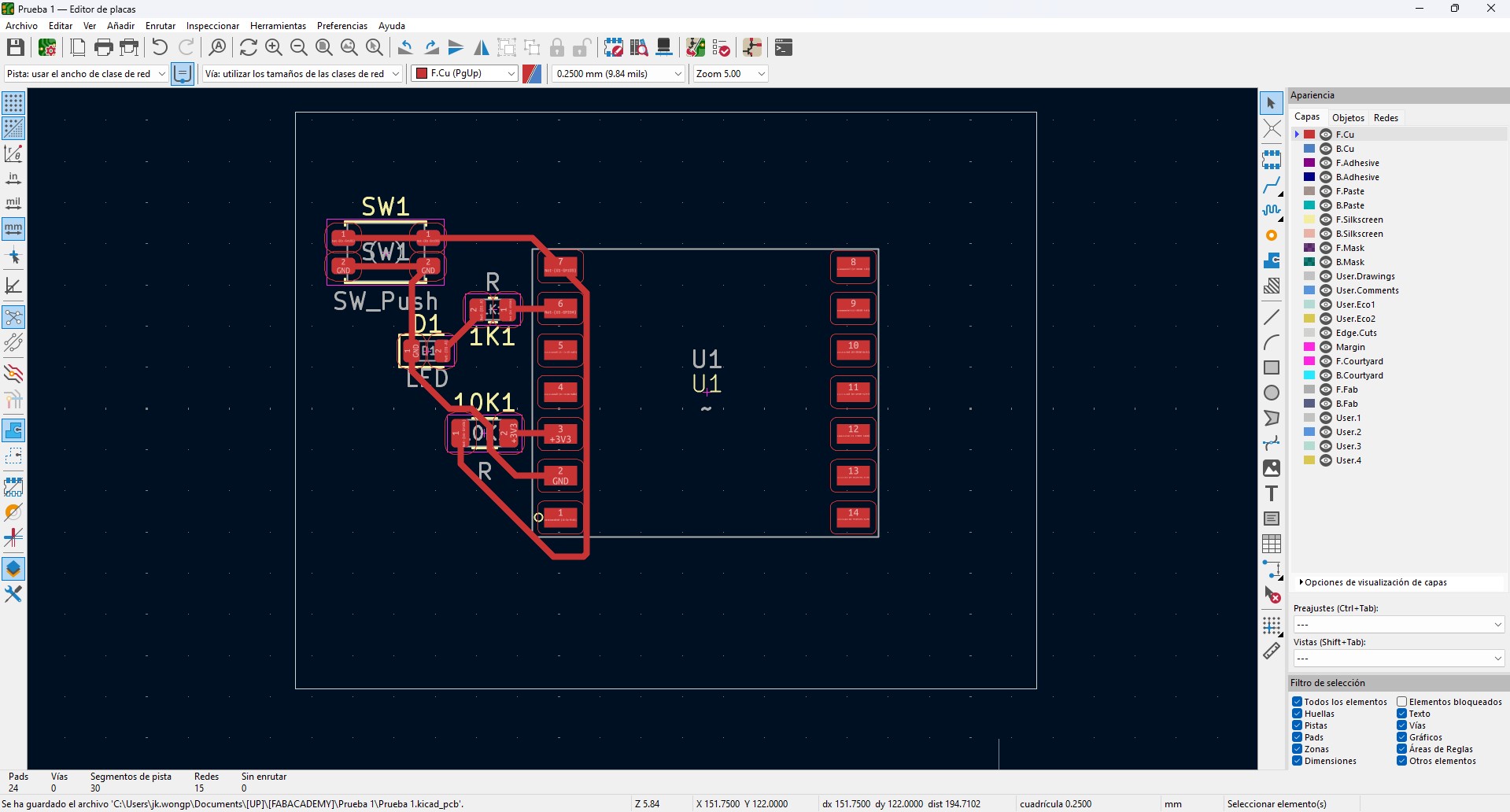
PCB layout prepared in KiCad before exporting the design as an SVG file.
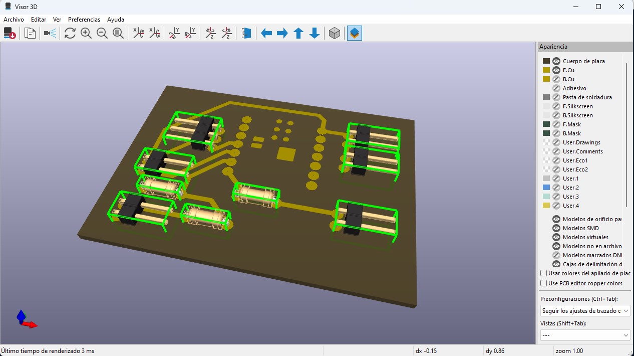
3D visualization of the PCB showing component placement and board configuration before fabrication.
2. Refining the Design in Inkscape
The SVG file was opened in Inkscape to prepare the geometry for fabrication. In this stage, the circuit traces are represented as vector shapes that define the areas to be preserved during the milling process.
First, the image was mirrored to ensure that the circuit would be correctly oriented when milled on the copper board. Additionally, some circuit paths were slightly opened so that the ground connections could properly merge with the rest of the copper surface.
SVG file edited in Inkscape showing mirrored design and adjusted paths for proper ground connection.
This step was essential because it refined the vector geometry and ensured that the design was correctly prepared for toolpath generation.
3. Generating the G-code
After refining the design in Inkscape, the next step was to generate the G-code, which contains the instructions required for the CNC milling process. This step translates the vector geometry of the PCB into toolpaths that define how the milling tool will move to remove copper and isolate the traces.
The toolpaths were generated based on the contours of the traces, following an isolation strategy. In this approach, the milling tool moves around the edges of the conductive paths, removing the surrounding copper while preserving the areas that form the circuit.
This process was carried out using a toolpath generation workflow within the Inkscape environment, where the vector design was interpreted to define the machining paths. Parameters such as tool diameter, cutting depth, and feed rate were considered to ensure that the generated paths were compatible with the physical characteristics of the CNC machine and the milling tool.
The resulting G-code defines the precise movements of the tool, including the regions where material must be removed to achieve electrical isolation between traces. Once generated, the file was prepared for visualization and execution in the CNC control software.
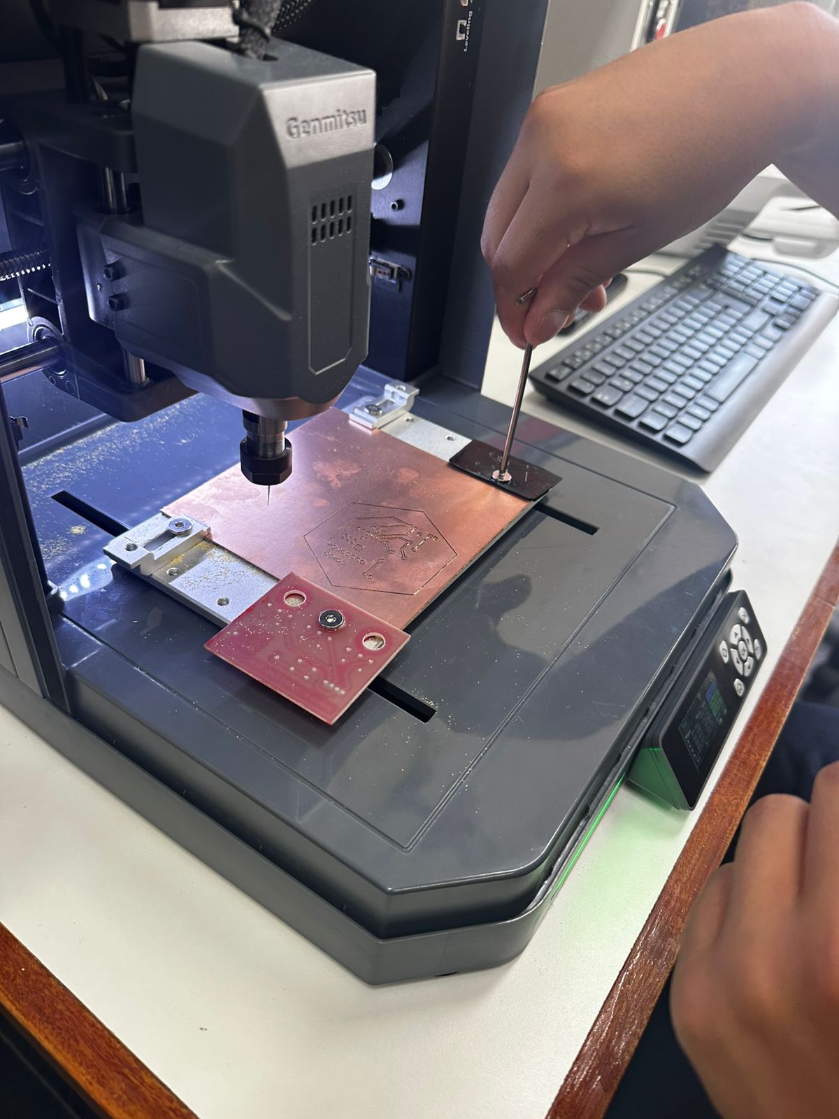
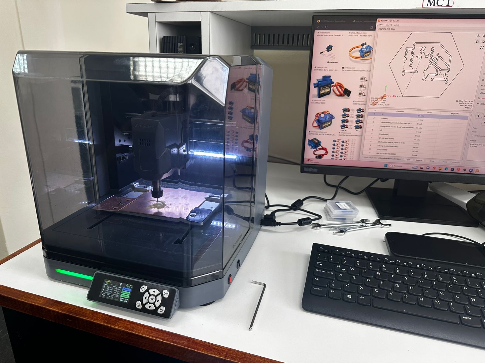
4. PCB Milling
To fabricate the board, a Genmitsu CNC milling machine was used.
Tool Geometry and Its Impact on Design
The milling process was performed using a V-bit engraving tool. This tool does not have a constant diameter; instead, its effective cutting width depends on the cutting depth.
This makes Z-axis calibration critical, since small variations directly affect the width of the cut and the isolation between traces.
For this reason, the selected design rules (0.4 mm clearance) provide a safety margin to ensure proper isolation.
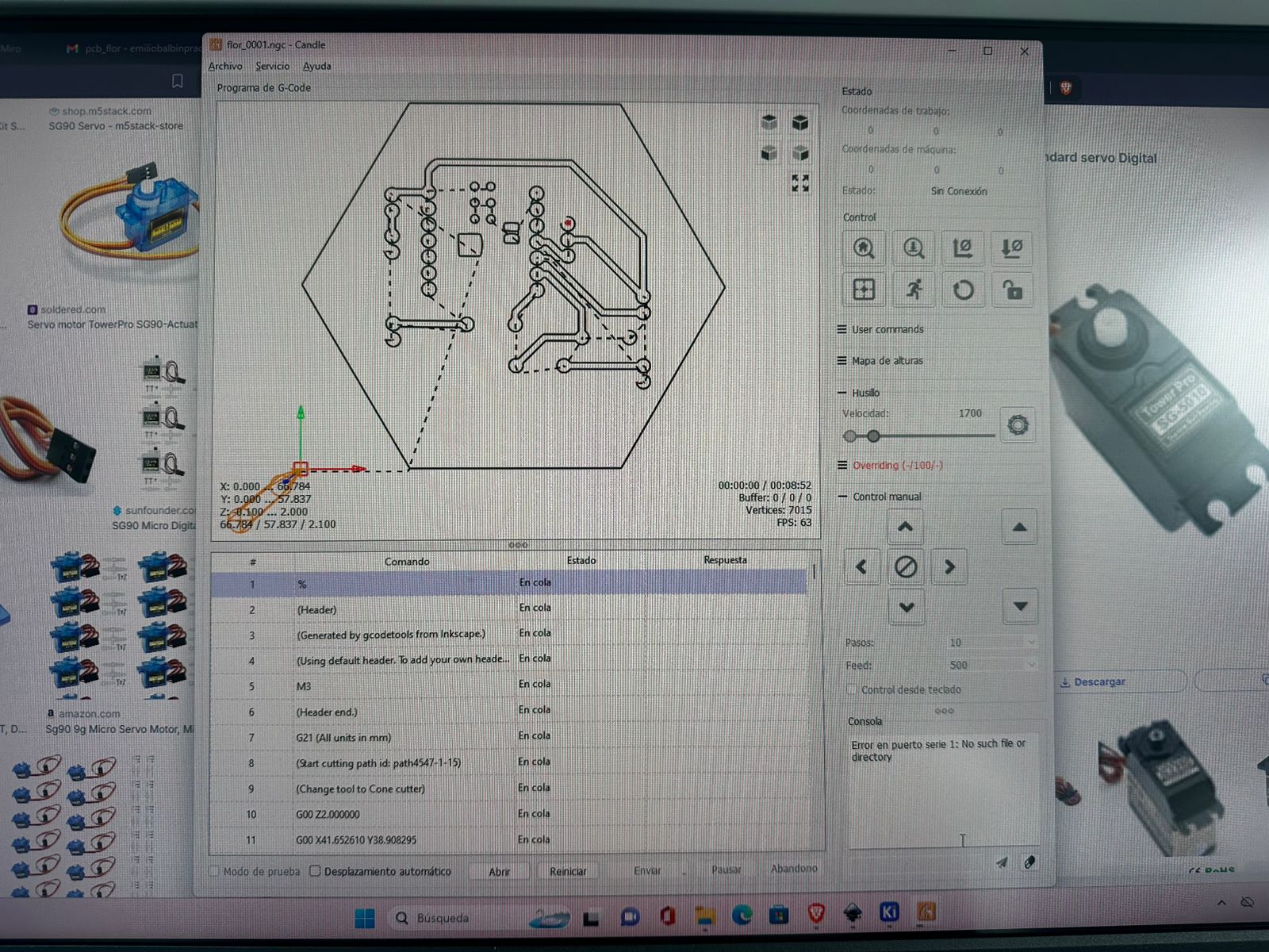
Candle Configuration and Machine Setup
The PCB board was fixed to the machine bed using double-sided tape to ensure stability. A V-bit tool was installed, and the Z-axis was calibrated manually.
- X and Y axes: positioned at the lower-left corner of the PCB.
- Z axis: calibrated manually by touching the copper surface.
Toolpath visualization in Candle used to verify the milling paths before executing the cut.
Milling Parameters
- Machine: Genmitsu CNC
- Software: Candle
- Tool: V-bit engraving tool (~0.1 mm tip)
- Feed rate: ~100 mm/min
- Plunge rate: ~50 mm/min
- Cutting depth: ~0.1 mm
These parameters were selected to ensure precise material removal and proper trace isolation.
During milling, the CNC removed copper around the traces, transforming the digital design into a functional circuit.
PCB milling process showing copper removal and trace isolation.
5. Drilling and Cutting the Board
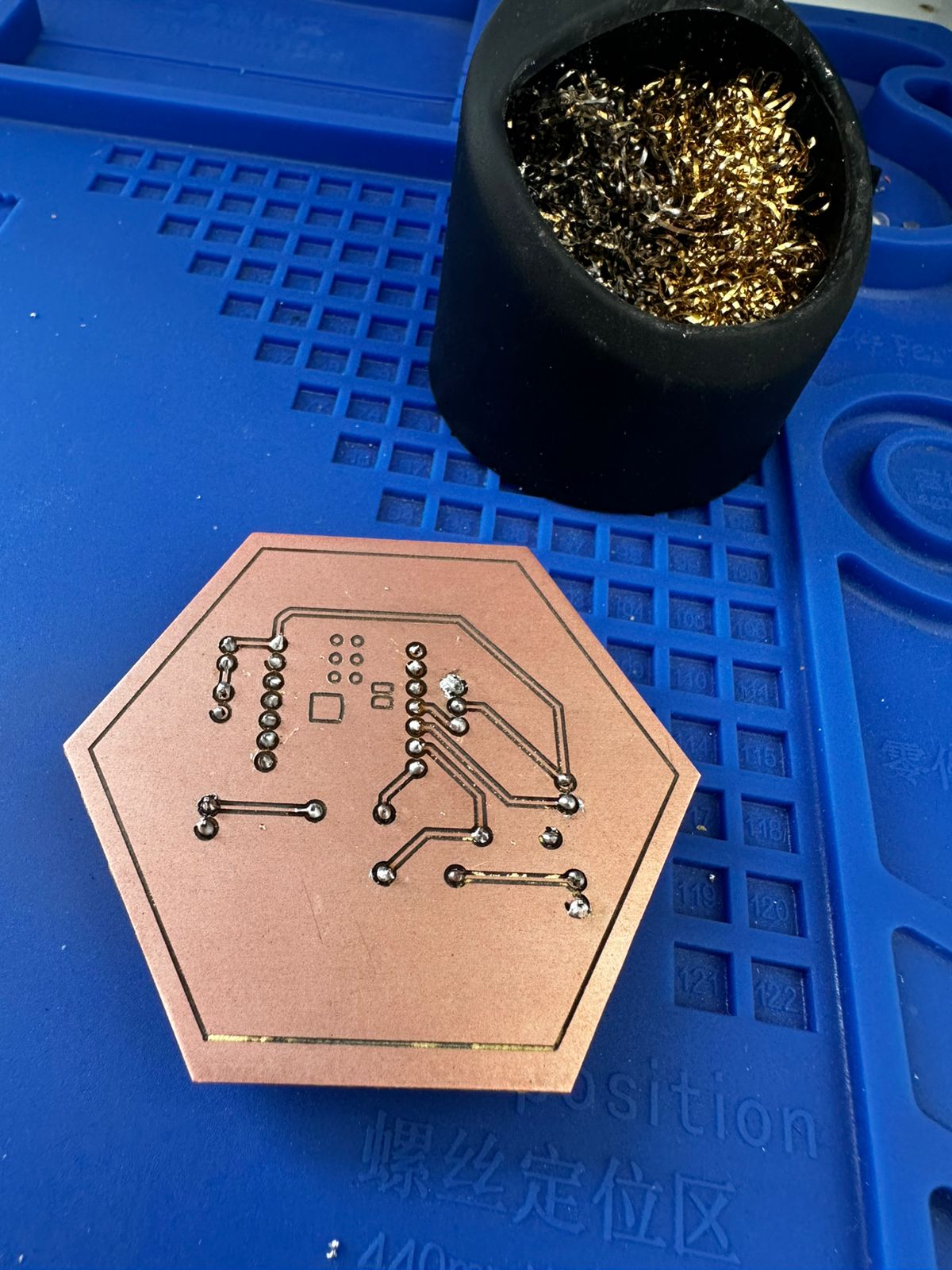
After the milling process was completed, the board was removed from the CNC machine and the required holes for the electronic components were drilled. A bench drill was used for this task in order to achieve precise and controlled holes for the component leads. Once the drilling process was finished, the board was cut to its final shape using a manual shear cutter. In this case, the PCB was trimmed into a hexagonal shape, which is part of the visual design of the electronic module.
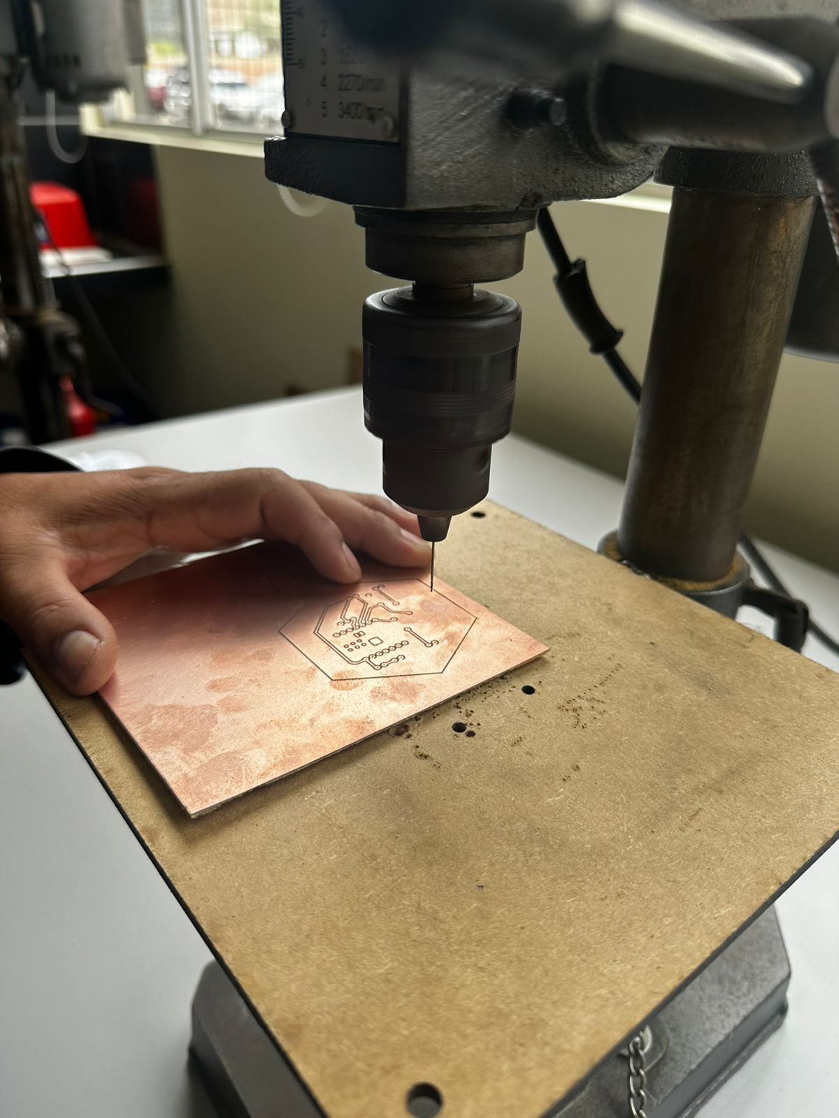
Drilling process of the PCB using a vertical drill press, where through-holes for electronic components are manually created after the milling stage.
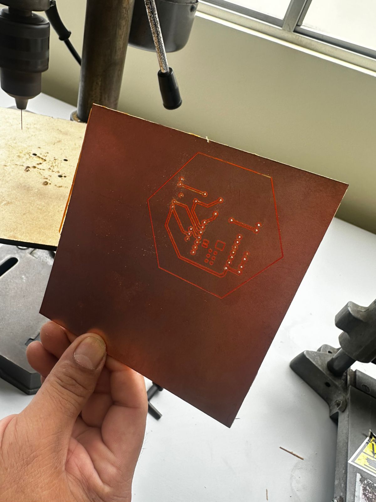
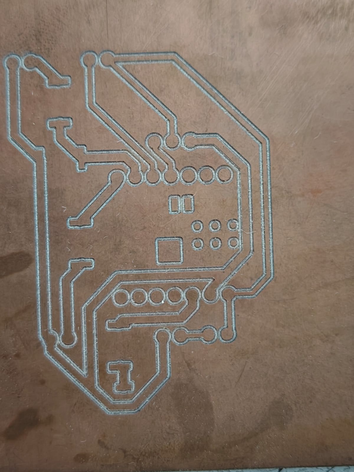
Milled PCB showing trace isolation and perimeter cut, where the copper has been removed around the traces to create the electrical circuit.
PCB cutting process using a manual shear cutter to define the final board dimensions and separate the piece from the larger copper sheet.
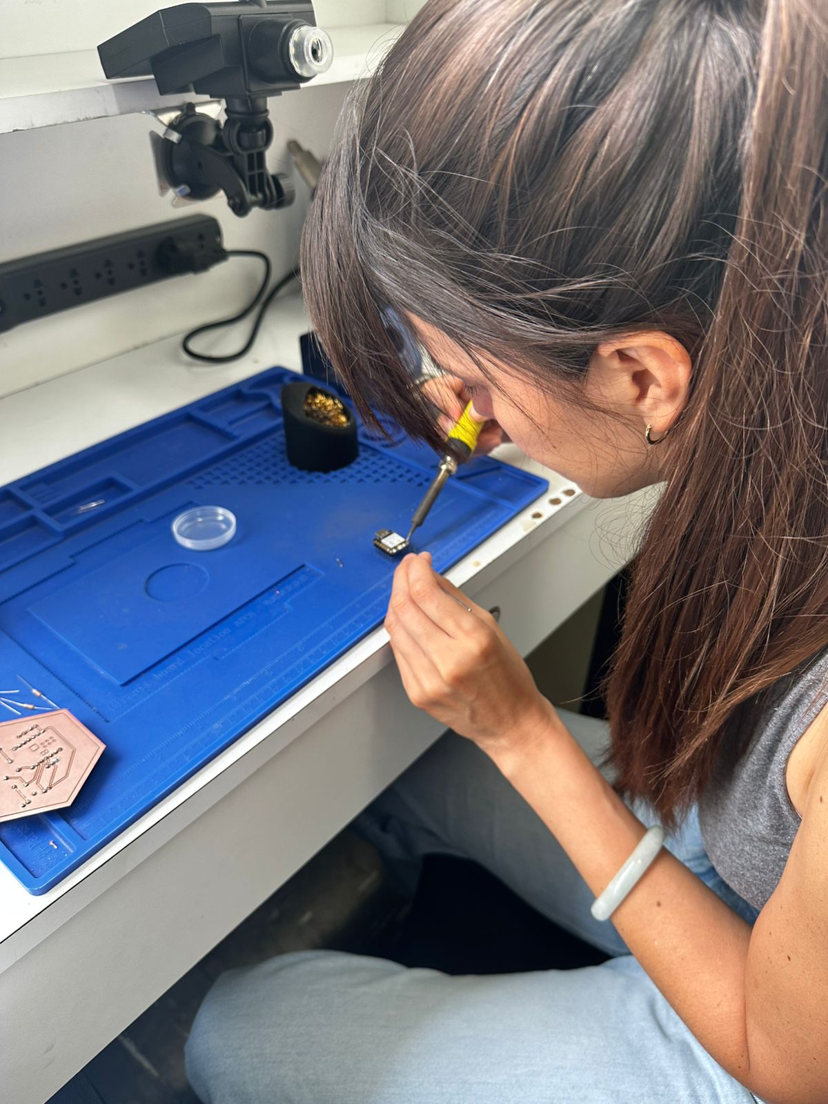
6. Component Assembly and Soldering
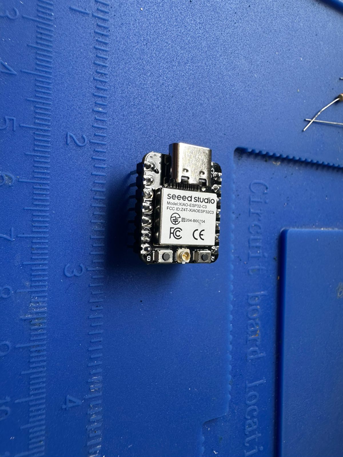
The next step was the assembly of the electronic components. The components used in this board include resistors, pin headers, LEDs, buttons, and the Seeed Studio XIAO ESP32-C3 microcontroller, which serves as the main controller of the circuit.
All components were soldered manually using a soldering station, solder wire, and cutting tools to trim the excess leads.
During the soldering process, special care was taken to control the temperature of the soldering iron and apply the correct amount of solder in order to avoid cold joints or unwanted bridges between traces.
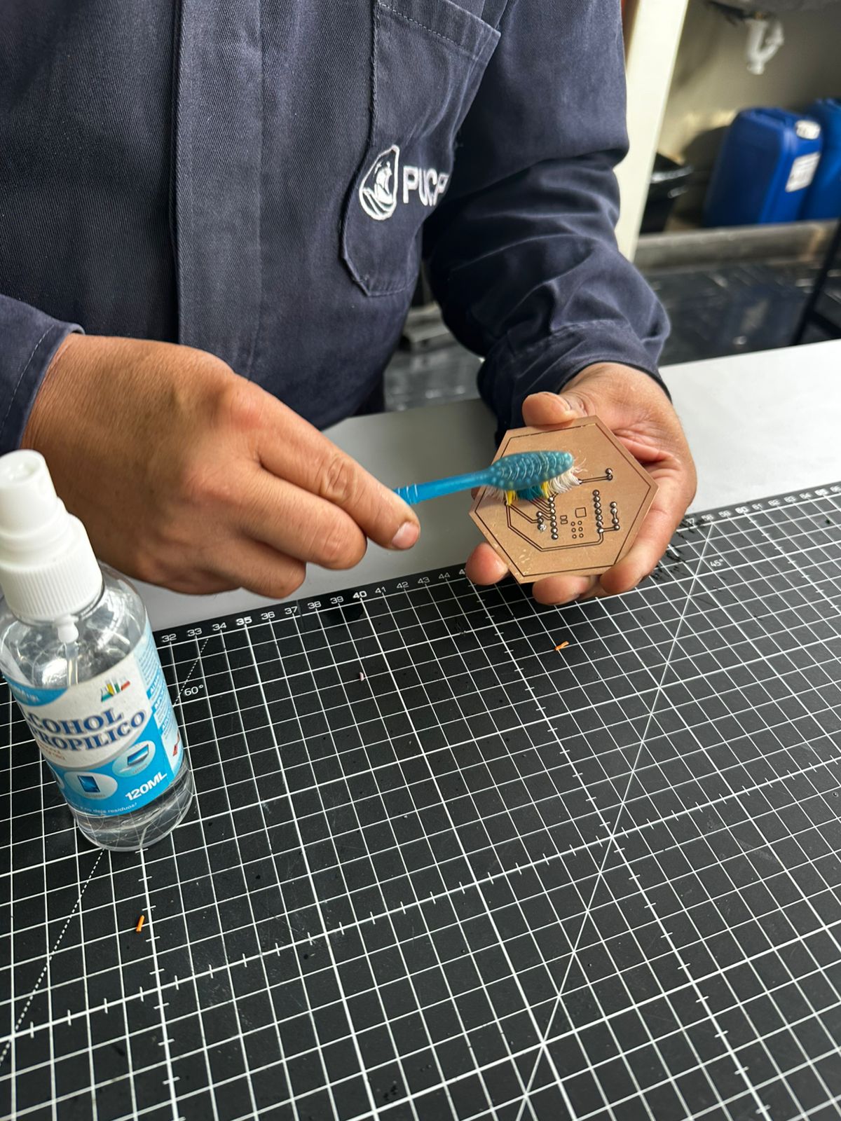
7. Cleaning the PCB
Before assembling the components, the PCB was cleaned using isopropyl alcohol and a brush. This step removes copper dust, grease, and residues from the milling process, ensuring good electrical contact during soldering.
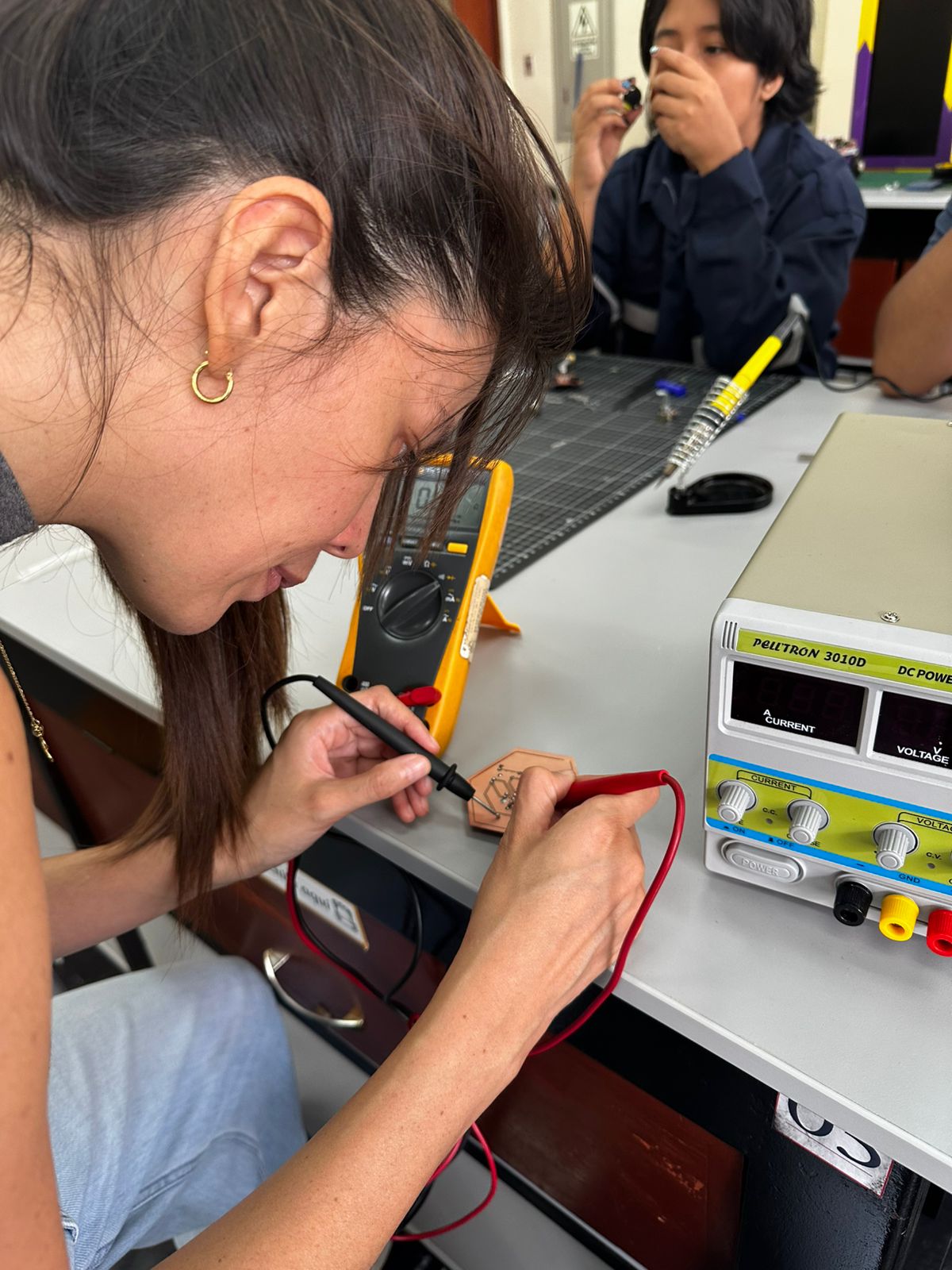
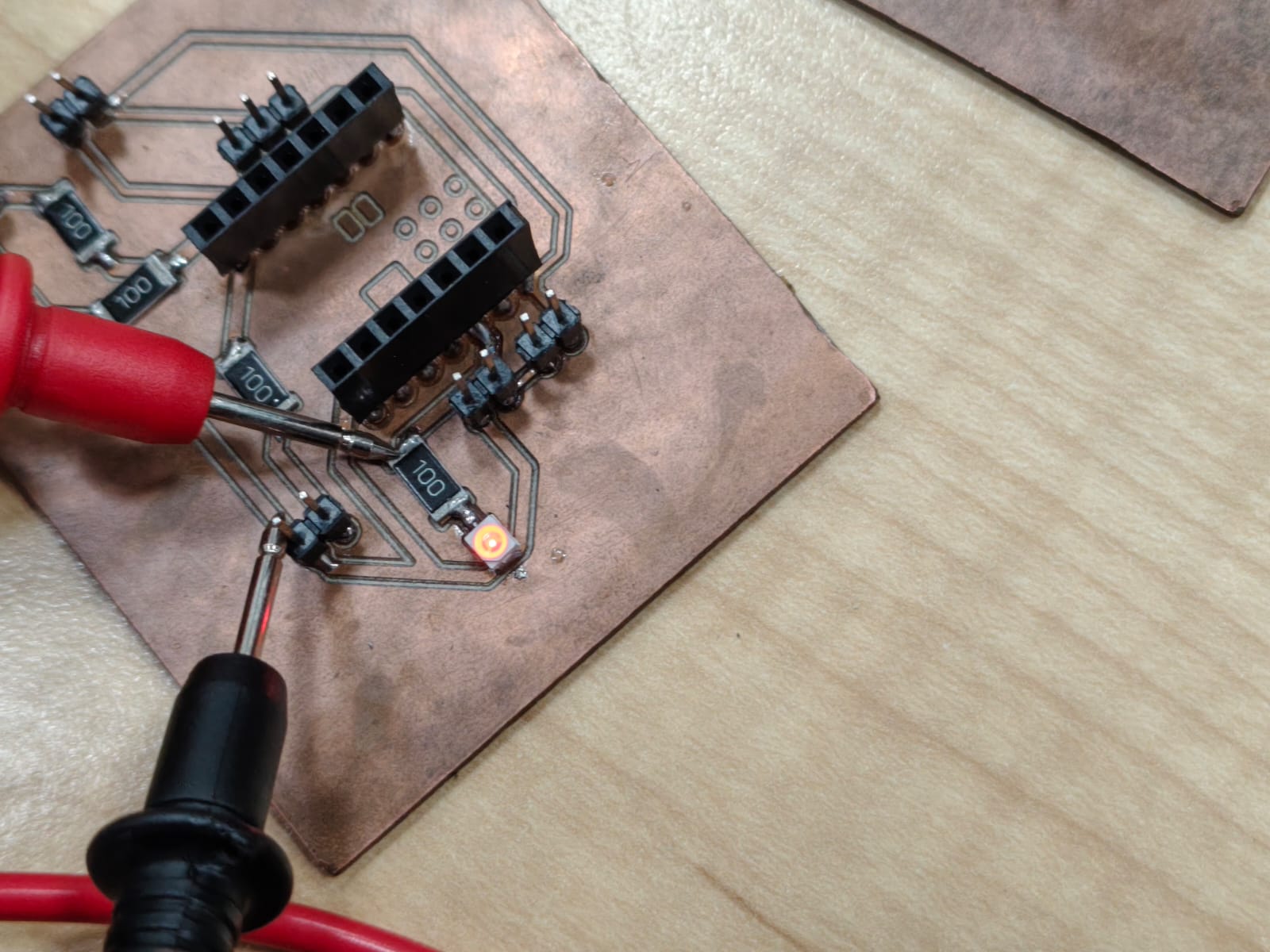
8. Electrical Verification
After completing the assembly, the circuit was tested using a digital multimeter and a power supply.
The verification process included checking the continuity of the traces, verifying the correct voltage supply, and ensuring that no short circuits were present. These tests confirm that the PCB was correctly fabricated and assembled before running the microcontroller program.
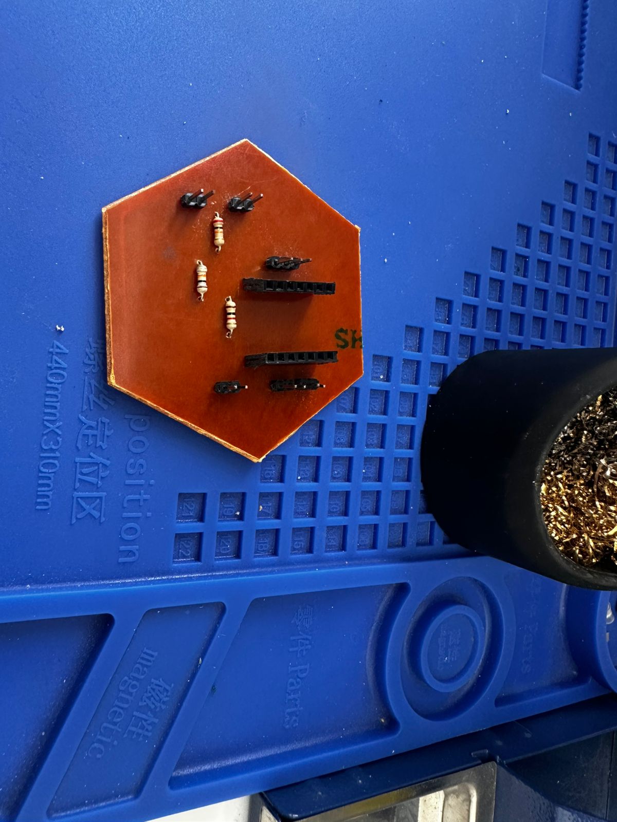
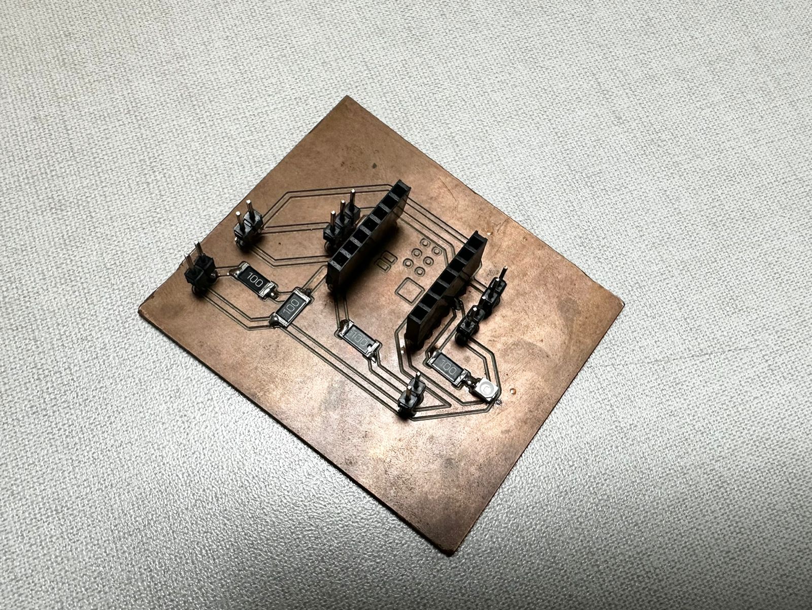
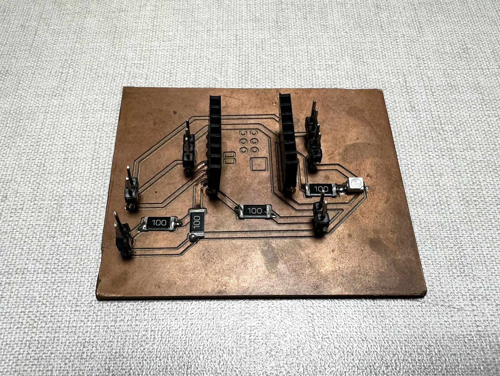
9. SMD Redesign and Assembly
The through-hole version was useful for understanding the circuit architecture, validating the connections, and performing an initial functional test. After successfully fabricating and assembling this version, a second iteration was developed using SMD (Surface Mount Device) components in order to gain experience with the fabrication and soldering techniques commonly used in modern PCB production and expected within the Fab Academy Electronics Production workflow.
9.1 SMD PCB Design
The SMD board was redesigned in KiCad, replacing the larger through-hole components with smaller surface-mount footprints. During this process, the routing was adjusted to maintain clear connections between the microcontroller pins, resistors, LED, and external connectors.
Special attention was given to the width and spacing of the traces, since the board would be fabricated using a milling process. The final layout kept the traces wide enough for reliable milling while also reducing the overall size of the circuit compared to the through-hole version.
9.2 Manufacturing File Preparation
Once the PCB layout was completed in KiCad, the design was exported and imported into the CAM software used to generate the milling toolpaths for the Roland SRM-20. This step translated the PCB geometry into machine instructions that could be interpreted by the CNC milling machine.
The traces, pads, and board outline were converted into machining paths using a PCB engraving workflow. Special attention was given to the isolation distance between traces and the dimensions of the milling tool to ensure that the final board could be manufactured accurately.
Before generating the final toolpaths, the design was reviewed to verify trace continuity, pad accessibility, and machining clearances. This verification helped prevent potential fabrication issues such as incomplete isolation or damaged traces.
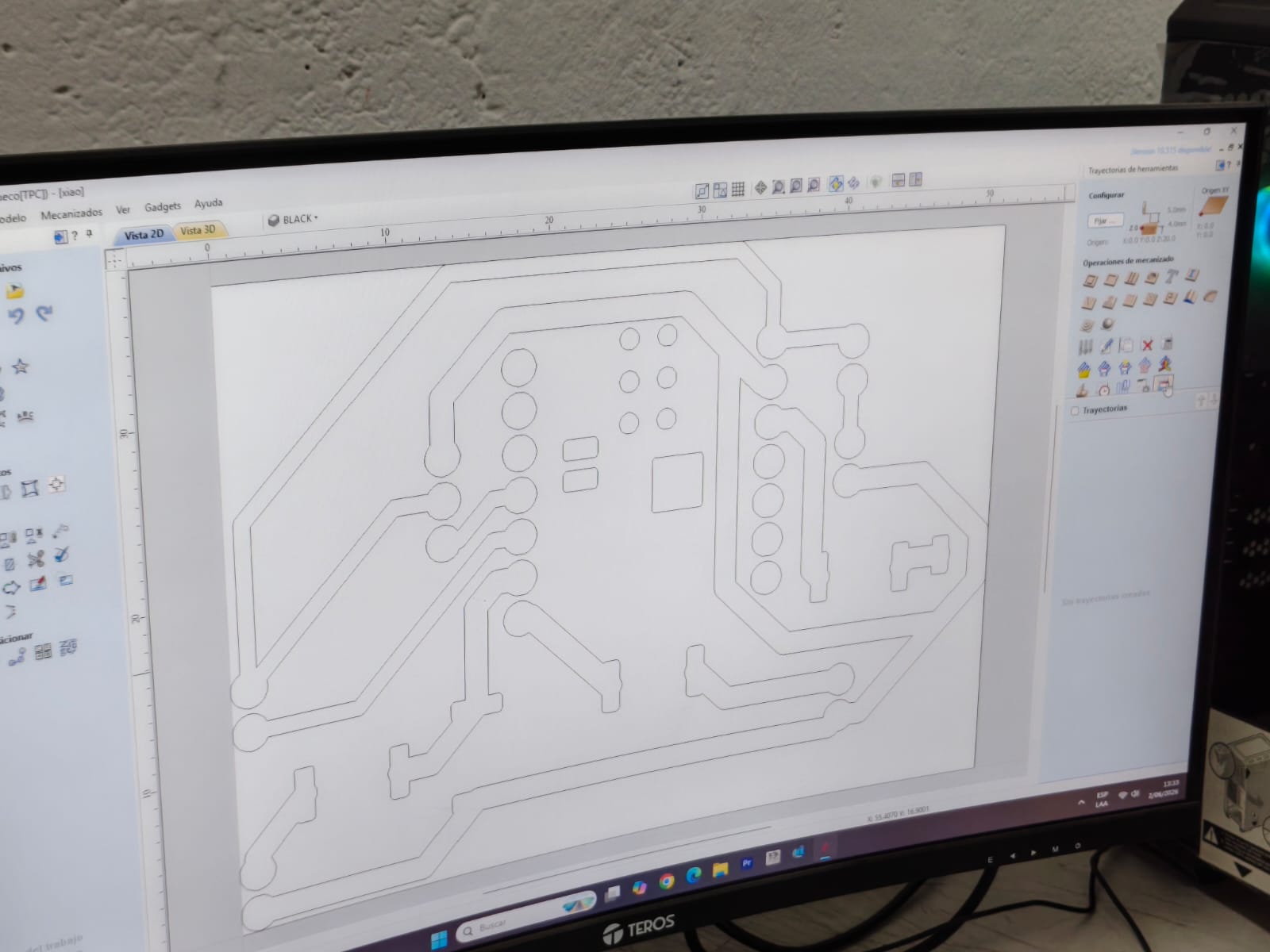
After defining the machining strategy, the toolpaths were generated and exported using the Roland postprocessor. The machining file included the engraving operations required to isolate the copper traces from the surrounding material.
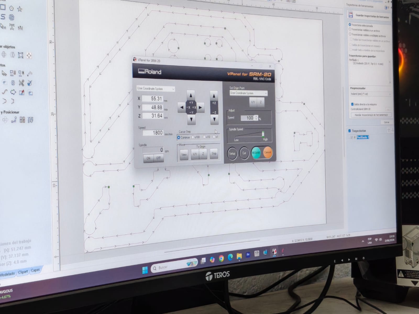
The final toolpaths were then loaded into VPanel for the Roland SRM-20, where the machine origin, spindle parameters, and work coordinates were configured prior to fabrication.
9.3 PCB Milling
During milling, it was important to verify the tool height and board alignment to obtain clean and continuous traces. Since SMD pads are smaller than through-hole pads, precision was more critical in this version. Any excessive milling depth or poor leveling could damage the pads or reduce the quality of the traces.
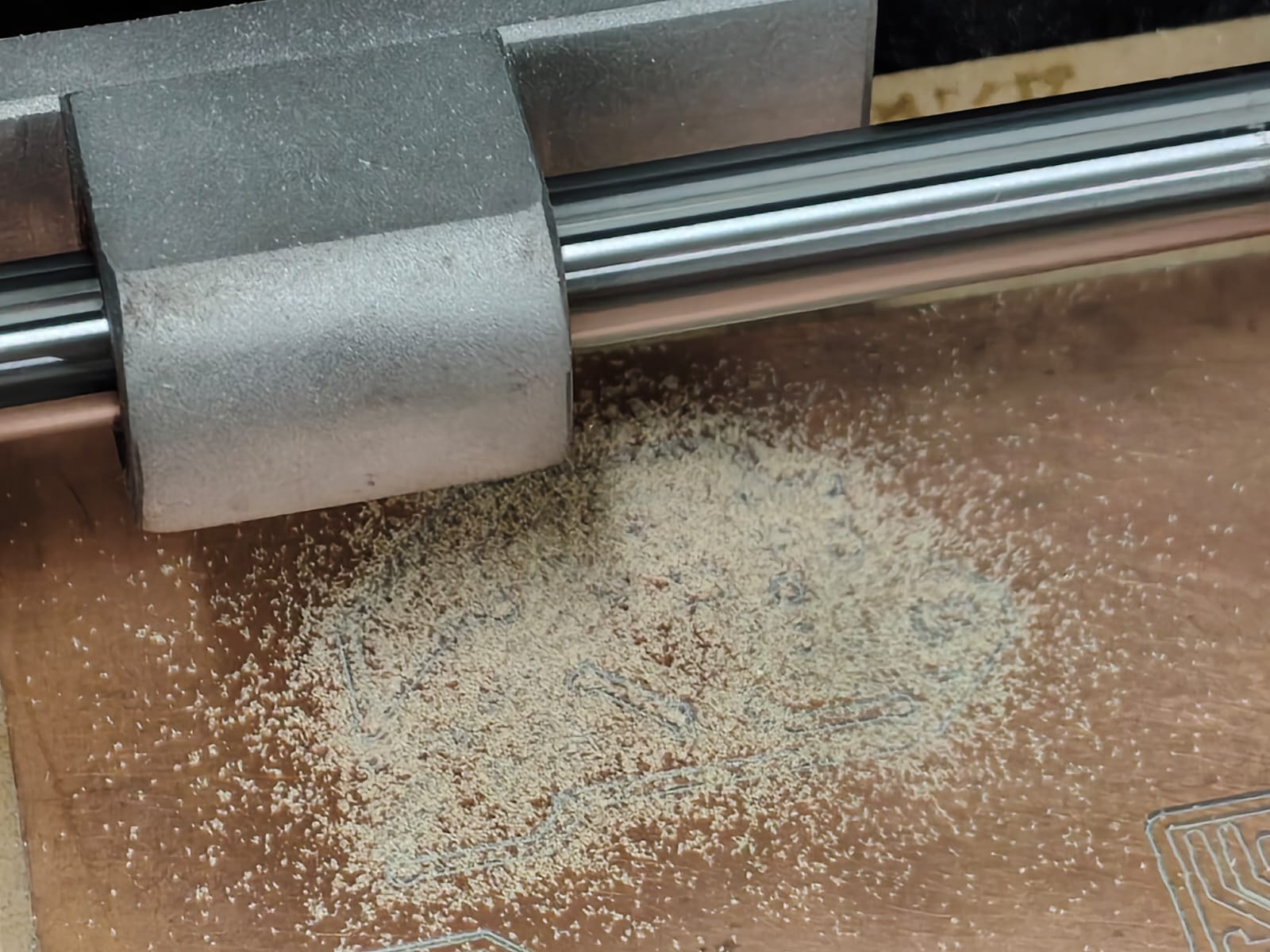
Some of the first attempts presented minor issues such as incomplete isolation, rough edges, or excess copper residue. These results were useful for understanding the importance of correct milling depth, tool condition, and surface leveling when producing boards with smaller SMD features.
9.4 SMD Soldering
Once the best milled board was selected, the SMD components were soldered onto the copper pads. This step required more precision than the through-hole version because the components are smaller and do not pass through the board. Instead, they are placed directly on the surface and soldered to the pads.
The process started by positioning the resistors and LED on their corresponding pads. A small amount of solder was applied to fix one side of each component first, allowing its alignment to be corrected before soldering the opposite side. After the passive components were placed, the pin headers were soldered to allow the board to connect with the rest of the system.
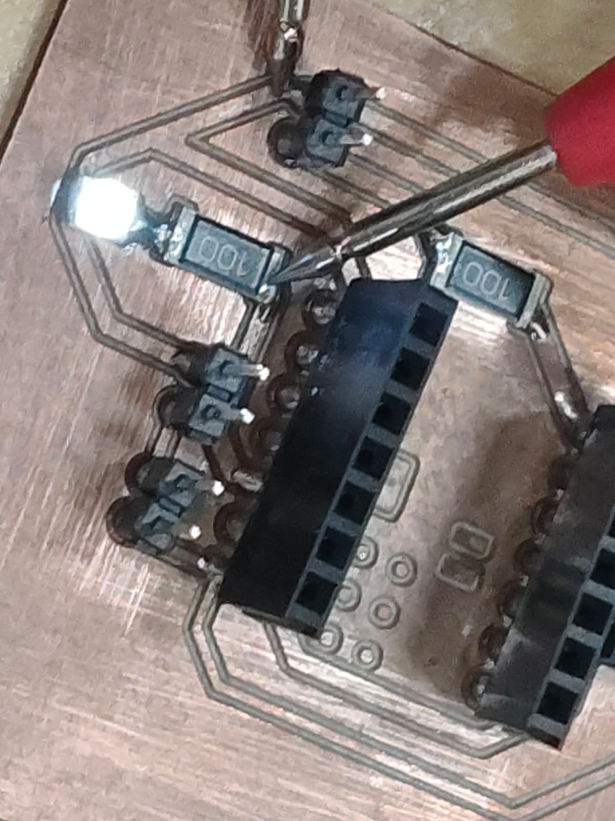
After soldering, the board was visually inspected to check for cold joints, bridges, or disconnected pads. A continuity test was also performed to verify that the traces were electrically connected where expected and isolated where necessary.
9.5 Electrical Testing and Validation
After completing the soldering process, the board was electrically inspected to verify the integrity of the circuit and identify potential assembly issues before connecting any external devices. Visual inspection was performed first to check for solder bridges, incomplete joints, component orientation, and possible short circuits between adjacent traces.
A multimeter was then used in continuity mode to validate the electrical connections between critical points of the circuit. This test confirmed that each trace was properly connected to its corresponding component and that no unintended connections had been introduced during the soldering process.
Special attention was given to the power distribution network and the LED circuit. Continuity measurements were performed between the power and ground lines to ensure proper isolation and prevent short circuits that could damage components during operation.
Once the continuity checks were completed successfully, the circuit was powered and functional tests were performed. The LED illuminated correctly, confirming that the power and signal paths were operating as intended. This test provided a simple but effective validation of both the PCB fabrication process and the quality of the soldered connections.
The testing stage demonstrated that the board had been successfully designed, fabricated, milled, assembled, and electrically validated. It also highlighted the importance of verification procedures in electronics manufacturing, where identifying issues before final integration can prevent failures and simplify troubleshooting.
10. Comparison Between Through-Hole and SMD Versions
Producing both versions of the board made it possible to compare two different approaches to PCB fabrication and assembly. The through-hole version was easier to handle and solder, making it useful for initial testing and debugging. In contrast, the SMD version required greater precision but resulted in a more compact and cleaner board.
| Through-Hole Version | SMD Version |
|---|---|
| Easier to solder manually | Requires more precision during soldering |
| Useful for first tests and debugging | More aligned with the Fab Academy electronics production workflow |
| Uses larger components and pads | Allows a more compact board layout |
| More tolerant to fabrication errors | Requires cleaner milling and better surface leveling |
| Good for learning circuit behavior | Good for practicing professional PCB assembly skills |
Reflection
This activity provided a comprehensive understanding of the complete PCB production workflow, from electronic design and PCB layout to CNC milling, component assembly, soldering, and electrical testing. It demonstrated how digital designs can be transformed into functional electronic devices through a combination of design, fabrication, and validation processes.
One of the most valuable aspects of this assignment was experiencing the transition from a digital schematic to a physical circuit. The milling process highlighted the importance of machine calibration, tool selection, and manufacturing parameters, while assembling and testing the boards reinforced the role of iteration and troubleshooting in electronics production.
Fabricating both through-hole and SMD versions provided insight into different manufacturing approaches. The through-hole board allowed rapid validation of the circuit, while the SMD version offered experience with the fabrication and assembly techniques commonly used in modern electronics production.
Overall, this project strengthened practical skills in PCB fabrication, electronics assembly, testing, and digital manufacturing, while demonstrating the complete workflow from design to a functional electronic system.
Download Files
The design files used in this assignment can be downloaded below.