
Week 08 — Electronics Production
Group Assignment
During this week’s group assignment, we explored and characterized the PCB fabrication workflow using the equipment available in the Electronic Laboratory of the Pontificia Universidad Católica del Perú (PUCP). The objective was to understand the complete process required to transform a digital circuit design into a physically manufactured printed circuit board.
This activity involved analyzing the different stages of PCB production, including digital design, generation of machining paths, CNC milling of copper traces, drilling, board cutting, and final cleaning. In addition to the fabrication sequence itself, we also evaluated the machine setup, tooling, software control, and machining parameters that directly affect the quality of the final board.
1. PCB Fabrication Workflow
The PCB fabrication process in the laboratory follows a sequence that transforms a digital design into a functional electronic board. The workflow begins with circuit design in an EDA software such as KiCad, followed by the generation of machining paths and G-code. Once the file is prepared, the copper-clad board is milled to isolate the traces, drilled where needed, cut to size, and finally cleaned.
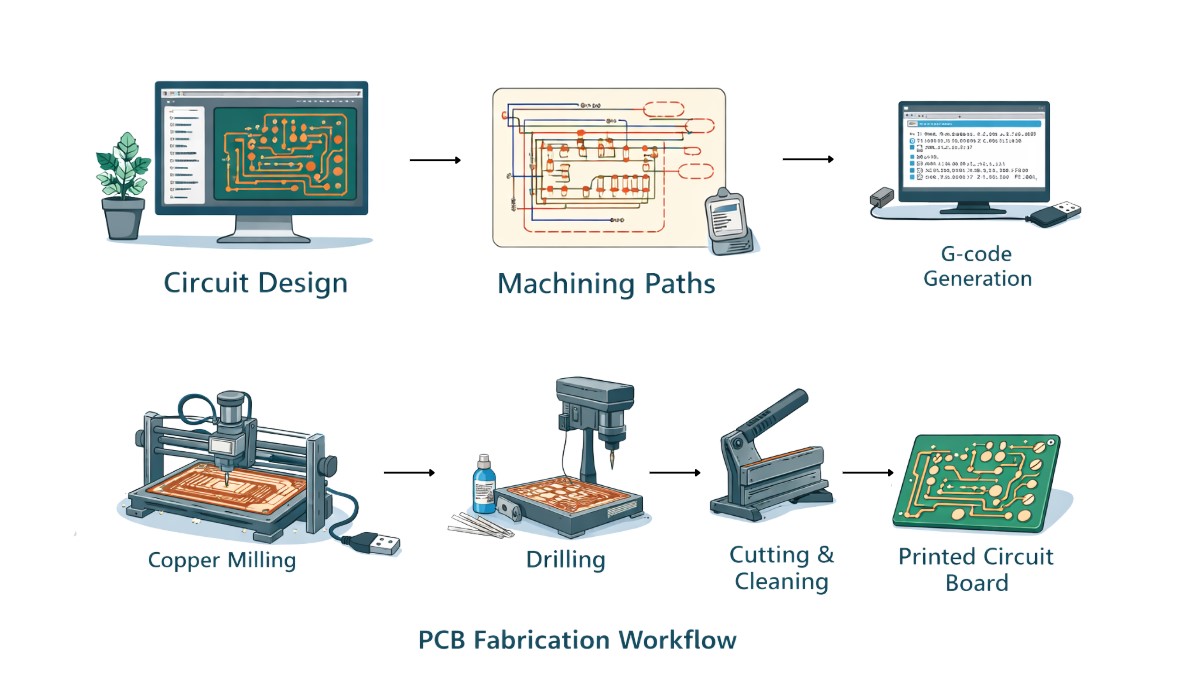
The main stages of the workflow were:
- Electronic circuit design in KiCad
- Export of the design and generation of machining paths
- Generation of G-code for the CNC machine
- Milling of copper traces to isolate the electrical connections
- Drilling of component holes
- Cutting the board to final dimensions
- Cleaning and inspection of the manufactured PCB
2. Main Machine Used: Genmitsu CNC Router
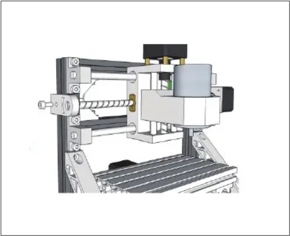
The traces were milled using a Genmitsu CNC router, a compact three-axis machine widely used for PCB prototyping. According to the Genmitsu 3018 user manual, the system includes an aluminum frame, linear axes, lead screws, stepper motors, spindle, ER11 holder, control board, USB cable, milling cutters, and a 24V power supply. This type of machine is well suited for PCB production because it allows controlled and precise surface milling on copper-clad boards.
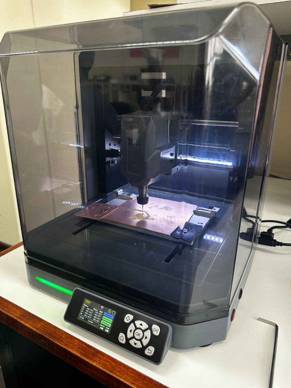
Main Characteristics
- Three-axis movement (X, Y, Z)
- G-code based numerical control
- USB communication with the computer
- 24V power supply
- ER11 tool holding system
- Compatibility with engraving and milling tools for PCB prototyping
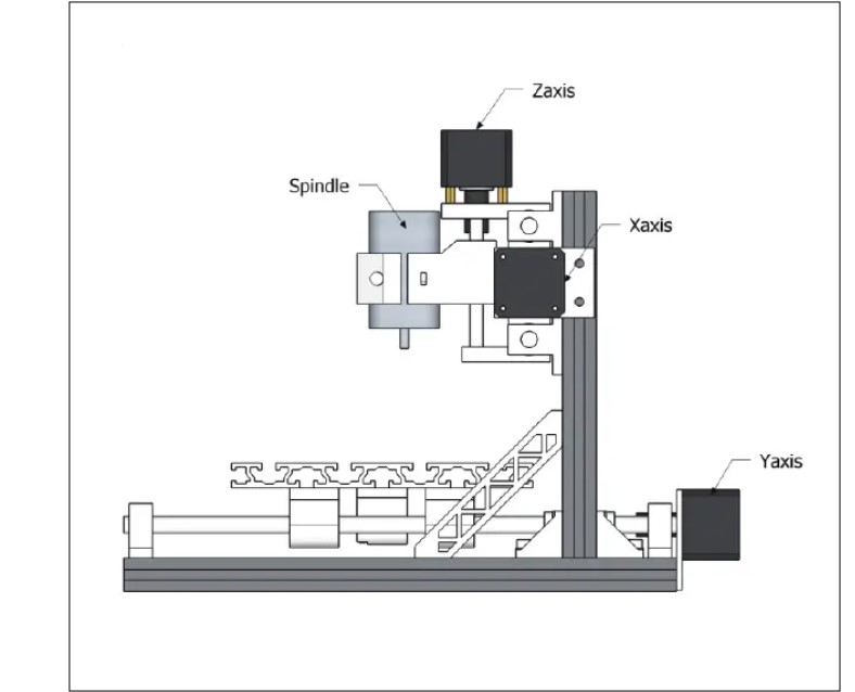
3. Machine Components Relevant to PCB Milling
Although the machine contains many structural and mechanical parts, some components are especially important for PCB production. The spindle and tool holder determine how accurately the cutter rotates; the stepper motors and axis system control movement precision; and the control board handles communication between the software and the machine. For PCB milling, this mechanical precision is critical because even small errors may affect trace isolation.
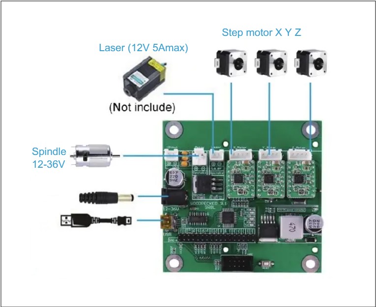
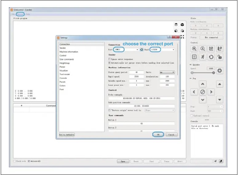
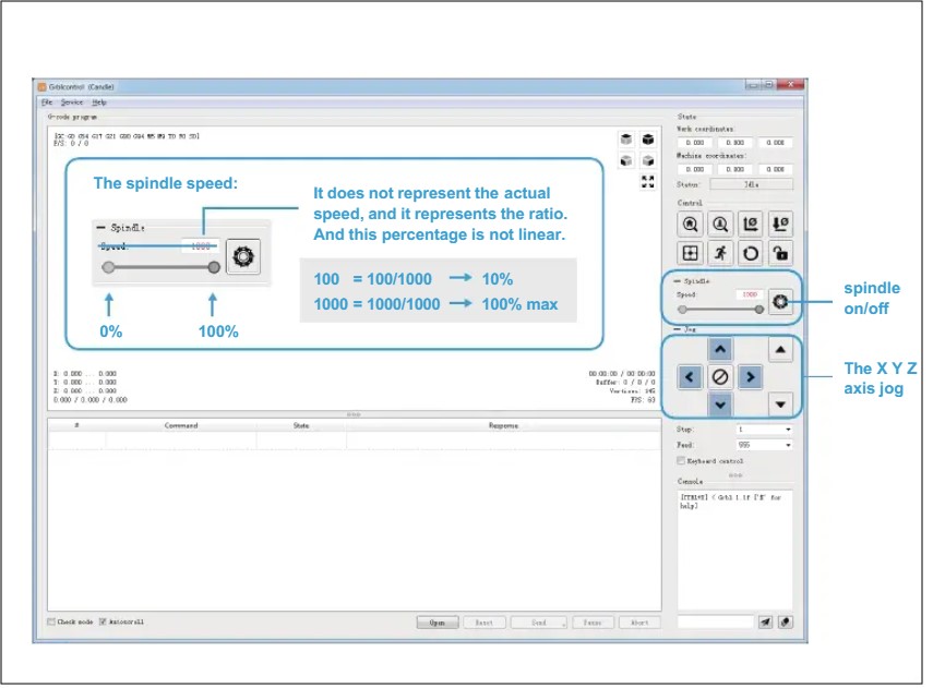
4. Software and Machine Setup
An important part of the characterization was understanding how the machine is prepared before the milling process. The Genmitsu 3018 manual explains that the CNC router is connected to the computer through USB and identified as a serial port. The software communicates with the machine controller, allowing the user to load the G-code, jog the axes, install the tool, and define the zero position before starting the job.
In PCB production, this setup stage is especially important because a small mistake in machine origin or tool height can completely affect the traces. For that reason, we considered software setup to be as important as the design file itself.
Setup sequence:
Connect machine → verify communication → install tool → fix board → jog axes → set zero XY → set zero Z → load G-code → verify toolpath → start milling.
5. Milling Process Characterization
During the group assignment, several machining variables were analyzed because they directly affect the quality of the final PCB. These variables determine whether the traces are clearly isolated, whether the copper is removed uniformly, and whether the board remains stable during fabrication.
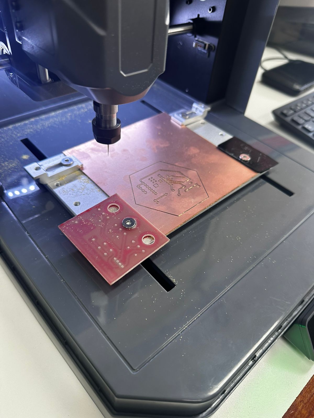
Cut Depth
Cut depth determines how much of the copper layer is removed. If the depth is too shallow, traces may remain electrically connected. If it is too deep, the machine may remove excessive material and damage the board substrate.
Tool Type
A V-bit engraving tool was used to isolate the traces. This type of tool is appropriate for PCB fabrication because it allows very fine and precise milling, which is necessary when working with small electronic paths.
Material Fixation
The copper-clad board must be fixed firmly to the machine bed. Even a small height difference or local warping can affect cutting depth and produce inconsistent isolation in different areas of the PCB.
Feed Rate
Feed rate influences both machining time and trace quality. If the speed is too high, the cuts may lose precision. If it is too low, the process becomes unnecessarily slow. Therefore, the feed rate must be chosen to balance accuracy and efficiency.
6. Complementary Machines
After the milling stage, two additional machines were used to complete the PCB workflow. These machines were essential for turning the milled board into a finished and usable part.
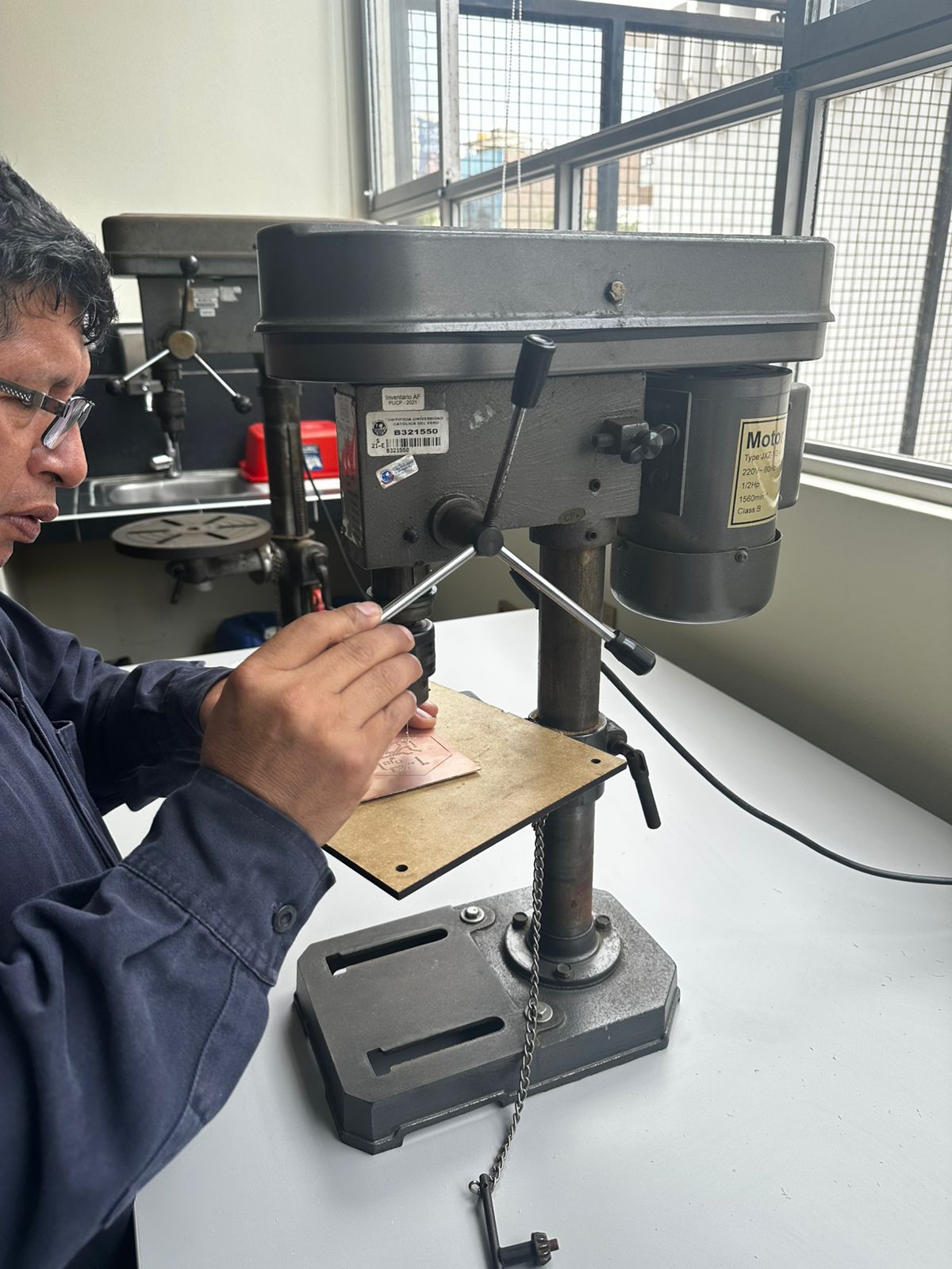
Bench Drill
A bench drill was used to produce the holes required for through-hole electronic components. This stage allowed accurate drilling with more control and precision than manual drilling.
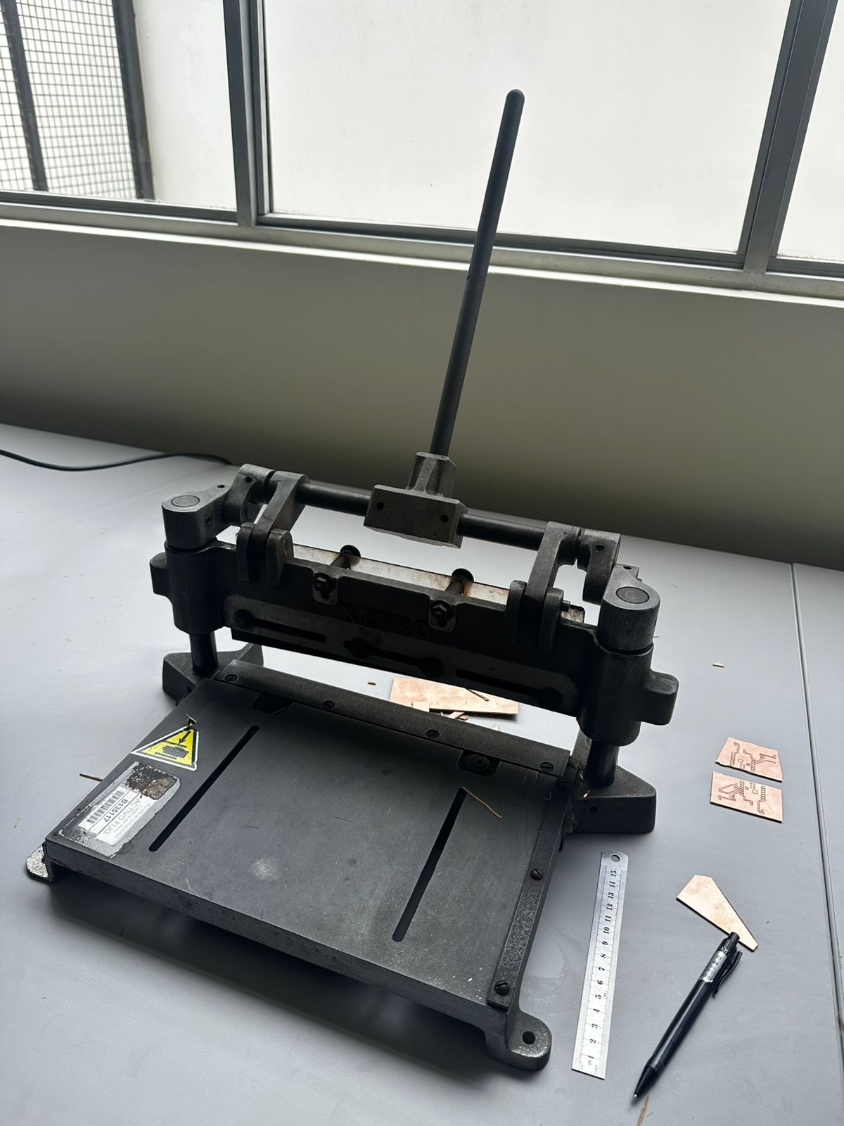
Manual Shear Cutter
Once the traces were milled and the holes drilled, a manual shear cutter was used to trim the board to its final size. This allowed a quick and controlled cut of the copper board without requiring an additional CNC contour operation.
7. Safety Considerations
PCB fabrication using CNC machines requires following basic safety procedures. Even though the machine is compact, it still involves rotating tools, sharp cutters, moving axes, and board fragments.
- Wear safety glasses during machining.
- Ensure the copper board is securely fixed before starting the machine.
- Verify that the milling tool is correctly installed.
- Keep the work area clean and free of loose objects.
- Do not place hands near the tool while the machine is operating.
- Never leave the machine unattended during operation.
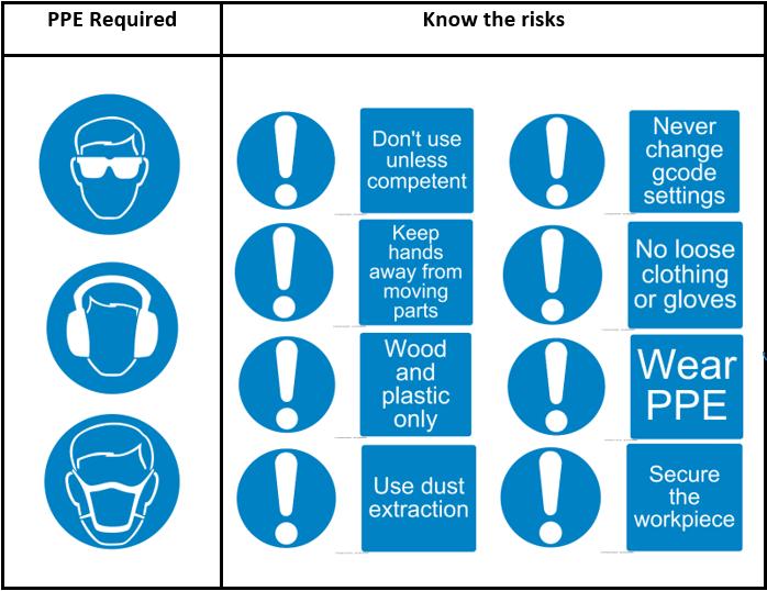
Safety note:
In PCB milling, precision and safety are closely related. A poorly fixed board or incorrect tool setup can affect both the result and the safe operation of the machine.
8. Group Learning Outcomes
This group assignment helped us understand that PCB production is not only a matter of electronics design. It also depends on machine setup, software control, tool installation, work zero definition, material fixation, and finishing processes.
Through this exercise, we learned that successful PCB fabrication requires integration between digital design, CNC machining, drilling, cutting, and safety practices. We also observed that in small-format CNC milling, proper setup is critical because even minor deviations can significantly affect trace quality.