
Week 6 — Embedded Programming
In Fab Academy, weekly assignments are documented as an evidence-based record of the tools used, decisions made, iterations, and results. This page documents my work for Week 6 — Embedded Programming, focusing on the electronics design workflow using KiCad to create a simple board based on the Seeed Studio XIAO ESP32C3.
The goal of this exercise was to design a small single-layer PCB prepared for copper milling. The board includes one LED with a current limiting resistor, a push button input, and a pull-up resistor connected to the 3.3V supply of the microcontroller.
Group Assignment
This week's group assignment consisted of using the test equipment available in the laboratory to observe the operation of a microcontroller circuit board. The objective was to analyze digital signals generated by the microcontroller and understand how communication between electronic components occurs.
During this activity we used measurement tools such as a logic analyzer to capture and visualize the digital signals produced by the microcontroller. This allowed us to analyze signal timing, logic states, and communication behavior within the circuit.
The complete documentation of the group work can be found in the following page:
Group assignment documentation
1. Installing KiCad
The first step was to download KiCad from the official website. KiCad is an open-source electronic design automation (EDA) software used to create schematics and PCB layouts.
After downloading the installer, the software was installed following the default installation wizard.
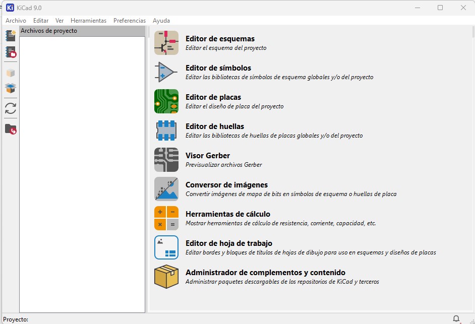
Once installed, KiCad provides several tools including the schematic editor, PCB editor, footprint editor, and symbol editor.
2. Creating a custom symbol for the XIAO ESP32C3
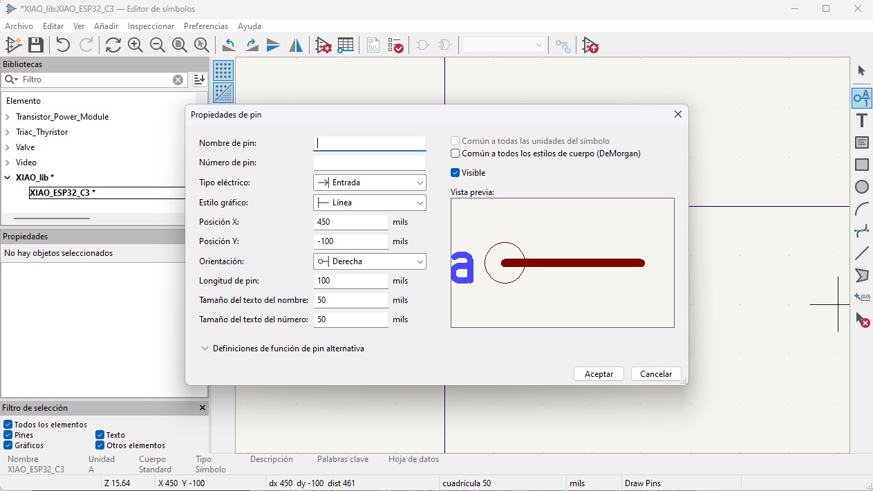
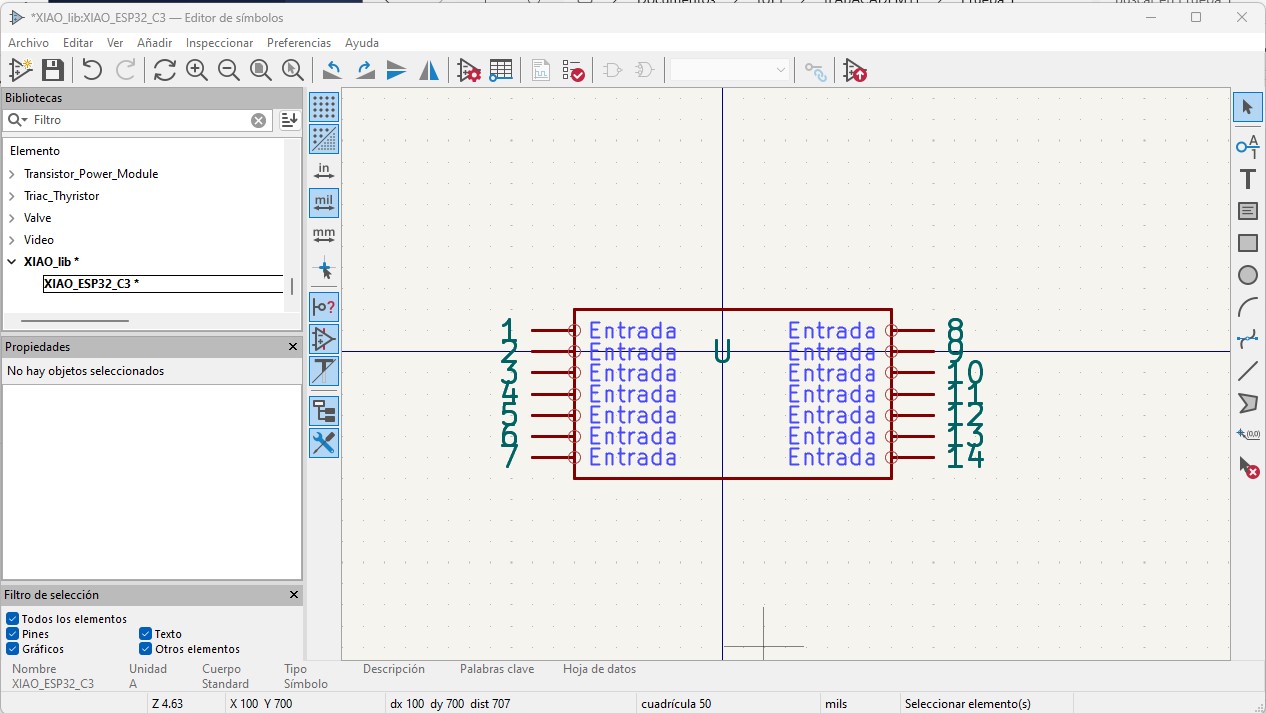
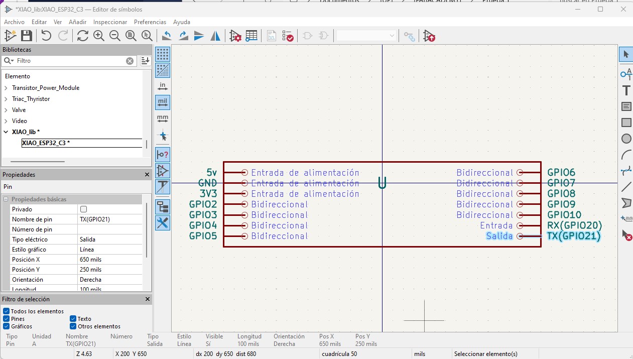
The XIAO ESP32C3 microcontroller is not included in the default KiCad libraries, so a custom symbol was created. A new personal library was generated and the symbol editor was used to define the pins corresponding to the module.
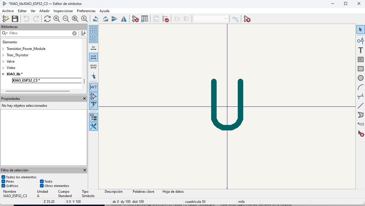
Each pin was configured with its name, number, electrical type, and orientation to ensure correct schematic behavior.
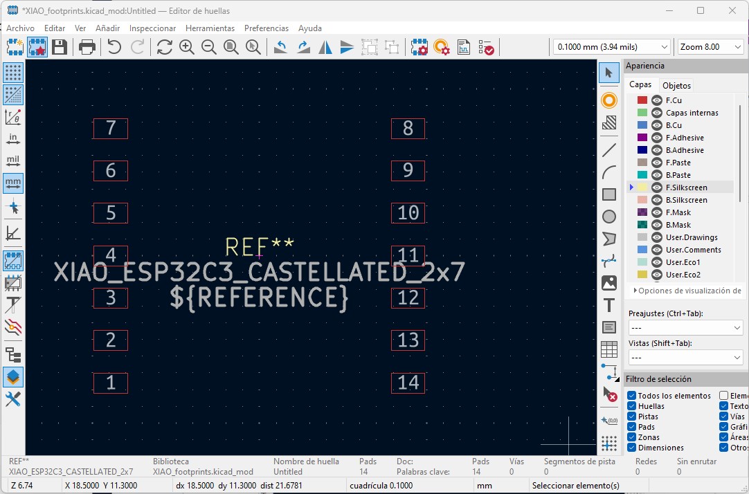
The final symbol contains fourteen pins arranged in two columns, representing the castellated pads of the XIAO ESP32C3 module.
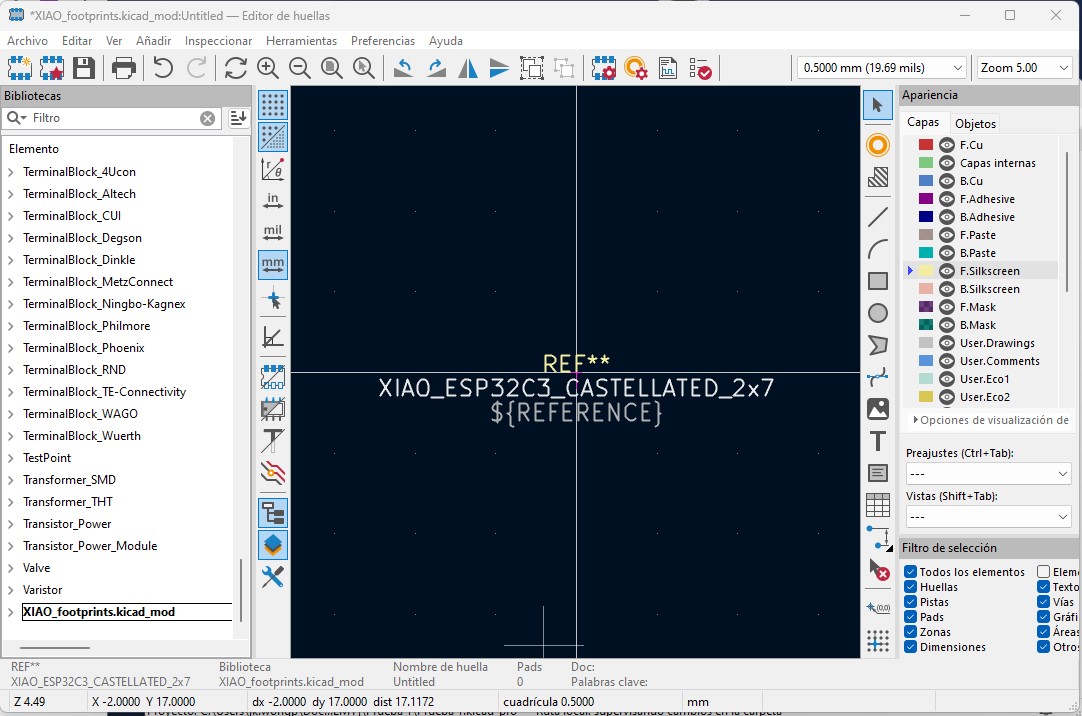
3. Creating the footprint
After defining the schematic symbol, a custom footprint was created to match the physical layout of the XIAO ESP32C3 module. The footprint was designed with two rows of seven pads to correspond with the castellated pads on the module.
The pads were carefully positioned to maintain the correct spacing and alignment. This ensures that the module can be soldered correctly once the PCB is fabricated.
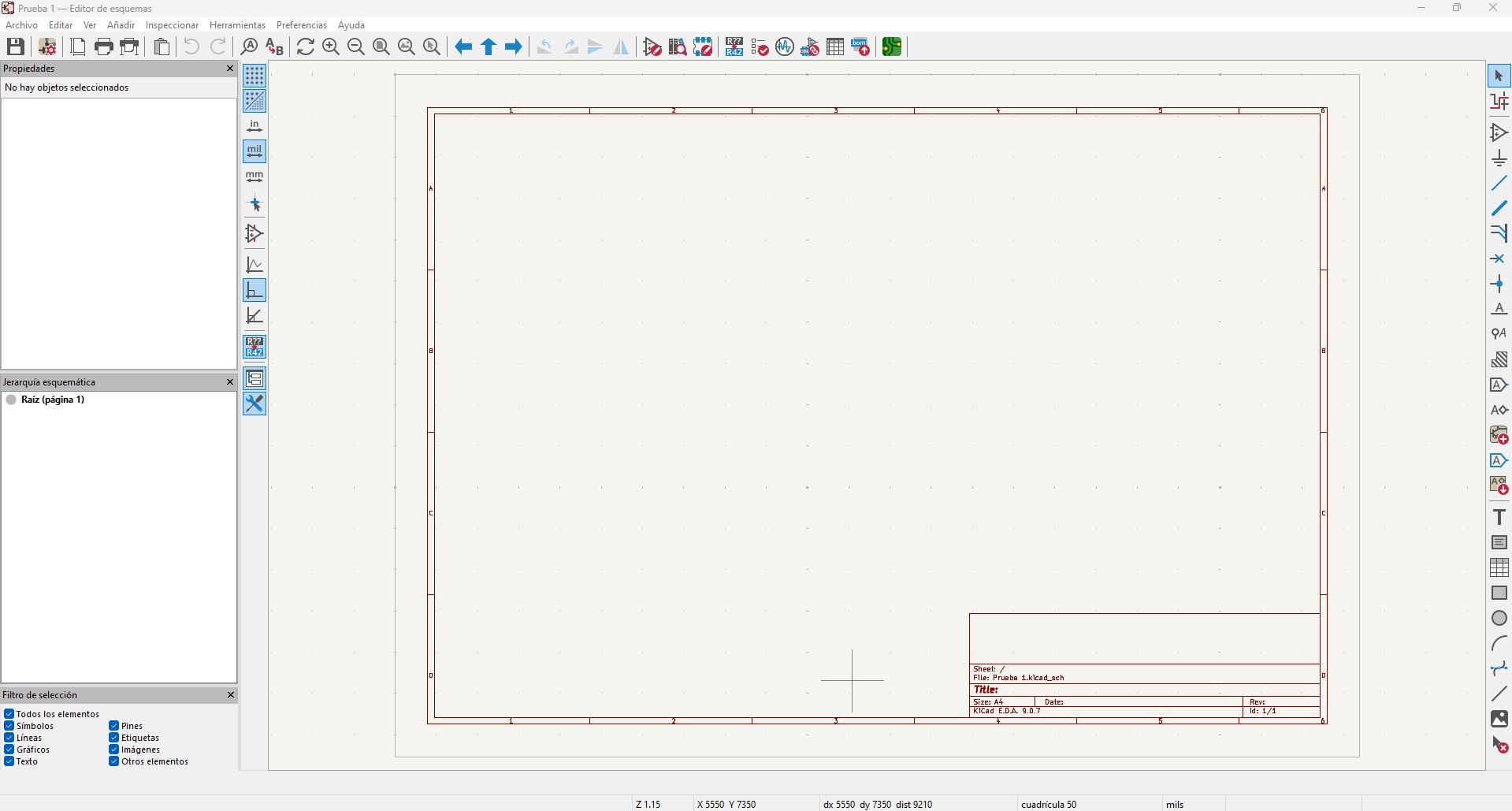
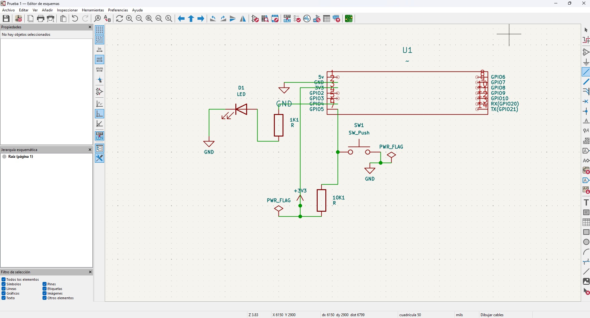
4. Creating the schematic
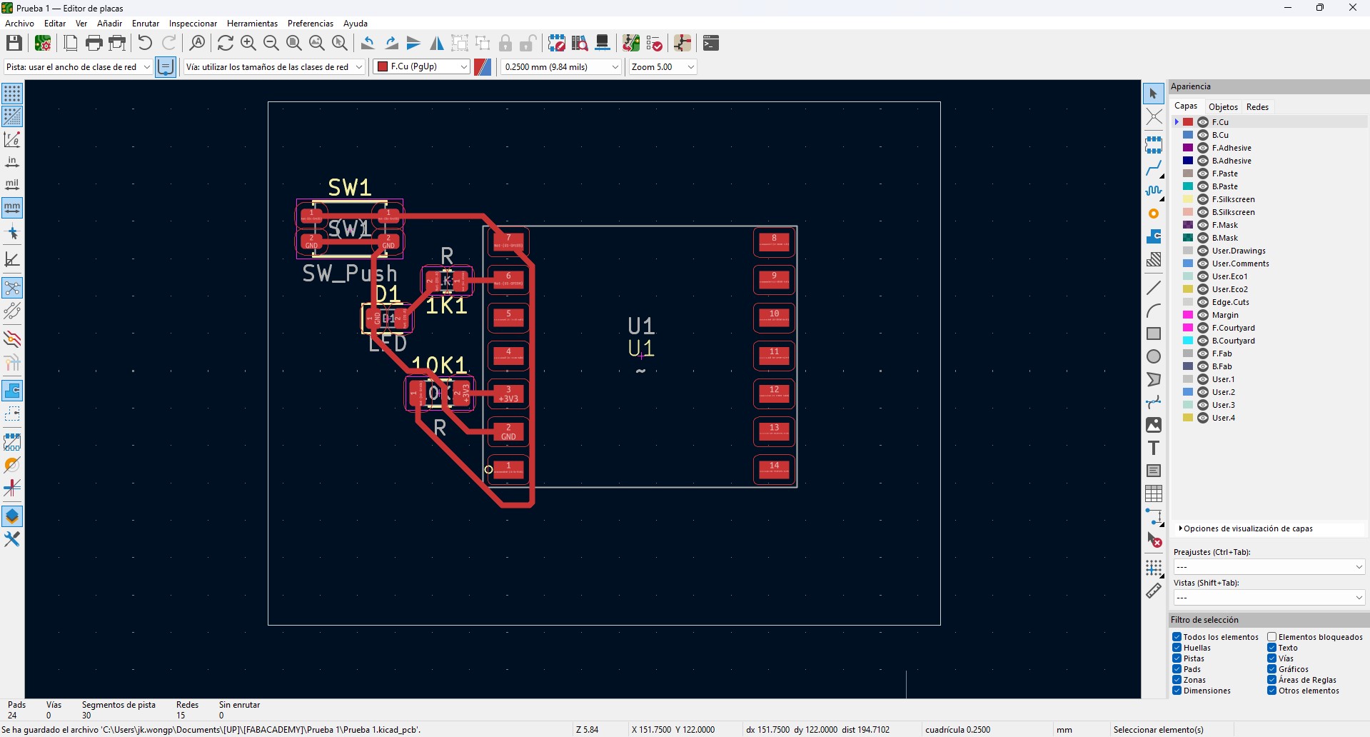
A new schematic sheet was created and the custom XIAO ESP32C3 symbol was placed. The circuit includes an LED output and a push button input.
The LED is connected to a GPIO pin through a 1kΩ resistor to limit the current. The push button is connected to another GPIO pin and includes a 10kΩ pull-up resistor to maintain a stable HIGH state when the button is not pressed.
5. PCB configuration and routing
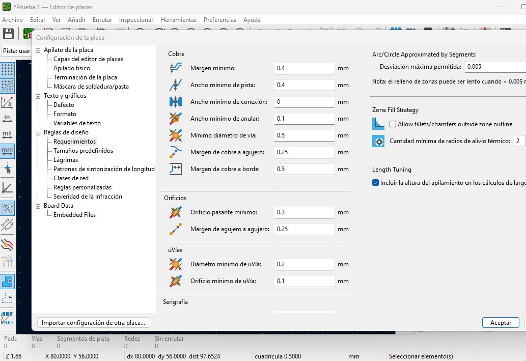
Before routing the board, the design rules were configured to match the constraints of the PCB milling process, including trace width and clearance values.
After importing the schematic into the PCB editor, the components were placed and the traces were routed on a single copper layer to simplify fabrication.
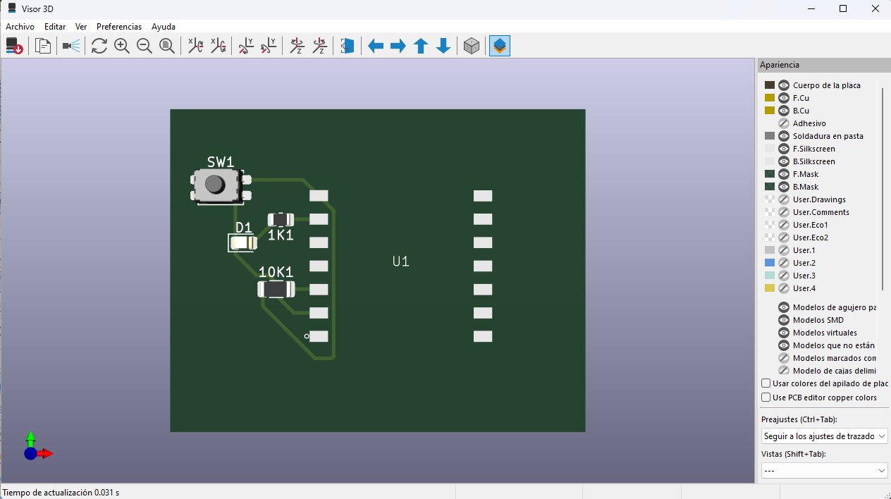
6. 3D verification
Finally, the 3D viewer was used to verify component placement, orientation, and spacing before manufacturing the board. The warnings generated by KiCad were ignored because they correspond to microcontroller pins that are not used in this specific circuit. The XIAO ESP32-C3 module includes several GPIO and auxiliary pins in its schematic symbol, but only a subset of them are required for this design, such as VBUS, GND, and the GPIO pins connected to the LED, button, and external headers. Some pins, such as B+ and B-, are included in the schematic symbol but are not present in the selected PCB footprint, which causes KiCad to report missing pad warnings when updating the board. Since these pins are not used for the operation of the circuit and all the required electrical connections are correctly routed, the warnings do not affect the functionality of the board and were therefore considered acceptable for this design.
Manufacturing considerations
The board was designed specifically for a milling workflow. The layout takes into account several constraints required for successful fabrication.
- Single-sided copper board
- No vias
- Trace width compatible with the milling tool
- Short routing paths to minimize milling time
Reflection
This assignment was challenging because it required learning several new tools and concepts simultaneously. Working with KiCad involved understanding the workflow between symbols, footprints, schematics, and PCB layout, which was initially confusing. Creating a custom symbol and footprint for the XIAO ESP32C3 required careful attention to pin configuration and alignment with the physical module.
Another difficulty was understanding the design rules and routing constraints needed for PCB milling, since the board must be designed with fabrication limitations in mind, such as trace width, clearance, and single-layer routing.
Although the process required several iterations and adjustments, it provided a better understanding of how electronic design translates from a schematic concept to a manufacturable PCB. However, I still need to continue experimenting with the software and the design workflow to confidently apply this knowledge to my final project.
In the next stages, I plan to refine my understanding of PCB design, test different component configurations, and integrate these electronic design skills into the development of my project.
Download Files
The design files used in this assignment can be downloaded below.