Assignment Requirements
Group assignment
- probe an input device's analog levels and digital signals
Individual assignment
- measure something: add a sensor to a microcontroller board that you have designed and read it
Progress Status
Sensor signal analysis and testing
Sensor integration and PCB fabrication
Full process documentation and debugging explanation
0) Group Assignment — Input Signal Analysis
As part of the group assignment for Week 09, we analyzed how input devices behave by probing both analog and digital signals. This involved understanding how sensors translate physical phenomena into electrical signals that can be interpreted by a microcontroller.
The group work focused on measuring and visualizing sensor outputs, identifying differences between analog and digital signals, and understanding how voltage levels vary depending on environmental conditions.
This process allowed us to better understand how input devices operate at a fundamental level, which directly supported the development of the individual assignment.
The complete group documentation can be accessed at the following link:
Fab Academy Lima — Week 09 Group Assignment
During this session, we also had an in-person meeting at Fab Lab UNI, where we discussed the results and coordinated the development of both the group and individual assignments.
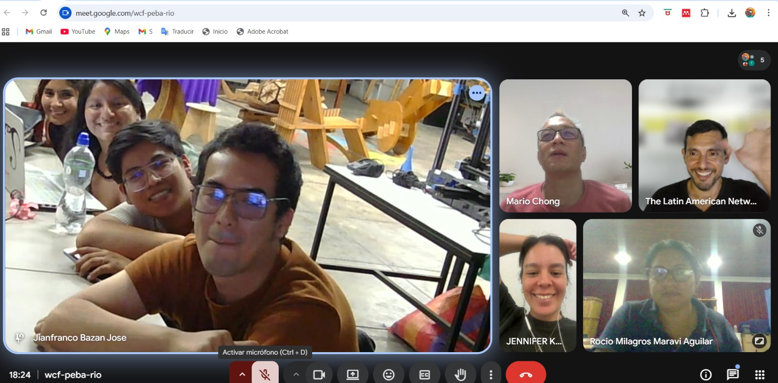
Group meeting session at Fab Lab UNI.
1) Individual Assignment — Measuring the Physical World
For this week’s individual assignment, the objective was to integrate a sensor into a custom microcontroller board and obtain measurable data from the environment. However, due to my limited experience in electronics, I decided to approach this assignment collaboratively alongside my classmate Carmen.
This collaborative approach allowed us to share knowledge, troubleshoot problems together, and accelerate our understanding of circuit design, sensor integration, and PCB fabrication. Additionally, both of us needed to develop sensors relevant to our final projects—light sensing in my case, and humidity sensing in Carmen’s case—so working together created a shared learning environment.
Rather than starting directly with fabrication, we structured our workflow in stages: component acquisition, simulation, prototyping, PCB fabrication, and debugging. This structured process helped us understand not only how sensors work, but also how to properly integrate them into a functional electronic system.

Initial planning and coordination with Carmen.

Early exploration of sensors and circuit ideas.
2) Component Acquisition and Design Constraints
Before starting the fabrication process, the first step was to define the components required for the project. Since both Carmen and I were developing sensor-based systems for our final projects, we decided to acquire the necessary electronic components locally in Lima.
We traveled to Jirón Paruro, a well-known electronics market in Lima where a wide variety of electronic components can be found, ranging from basic resistors and sensors to more specialized modules and microcontrollers. This visit was essential because it allowed us to physically inspect components, compare options, and adapt our design decisions based on real availability rather than theoretical assumptions.
This step introduced an important real-world constraint: unlike controlled laboratory environments, component availability in local markets can directly influence the design of a project. This forced us to be flexible and adapt our design strategy accordingly.
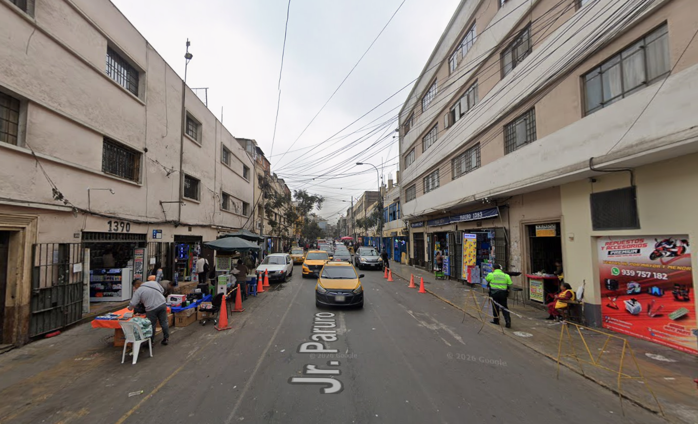
Visit to Jirón Paruro electronics market in Lima.
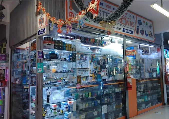
Exploration of available electronic components.
2.1 Components Purchased
During this visit, I acquired several components that would be used not only for this week's assignment, but also as part of the development of my final project. The selection of components was based on both functional requirements and availability in the local market.
The main components purchased were:
- 4x Servo motors (for future actuation systems)
- Photoresistor (LDR) module (light sensor input)
- Humidity and temperature sensor
- Voltage regulator
- Resistors and electronic support components
- Jumper wires and connectors
- Microcontroller: Xiao ESP32C3
Electronic components acquired for the project.
2.2 Material Constraints — PCB Selection
After acquiring the electronic components, the next step was to obtain the material required for PCB fabrication. Initially, our intention was to work with double-sided copper PCB (double layer), since this would allow more complex circuit routing and cleaner layouts.
However, during our search, we encountered an unexpected limitation: double-sided copper boards were not readily available in the local market. According to vendors, this material has become difficult to source due to reduced import availability, making it a relatively scarce and highly requested product.
Because of this limitation, we had to adapt our design strategy and work with single-sided copper PCB (one-layer board) instead.
This decision significantly impacted the circuit design process. Unlike double-layer boards, single-layer PCBs require careful routing to avoid overlapping traces. This often involves creative solutions such as using resistors or jumpers to "bridge" connections that would otherwise require a second copper layer.
This constraint became a key learning moment, as it forced us to think more critically about circuit layout and understand how to design efficiently within real-world limitations.
Single-sided copper PCB used for fabrication.
Comparison and evaluation of available PCB materials.
2.3 Design Implications
The limitation of using a single-layer PCB required us to rethink how circuits are designed. Unlike ideal conditions where multi-layer boards simplify routing, here we had to carefully plan trace paths to avoid intersections.
This also introduced the concept of using components strategically as part of the routing process. For example, resistors can be placed in such a way that they allow signals to "jump" over other traces, effectively acting as bridges in the circuit.
This experience highlighted an important principle in digital fabrication and electronics: design is always conditioned by fabrication constraints.
Rather than being a limitation, this became an opportunity to better understand how electronic systems are physically constructed and how design decisions must adapt to available resources.
2.4 Sensor Prototyping — Breadboard Testing
Before proceeding to PCB fabrication, we decided to validate our circuit logic through a prototyping phase using a breadboard. This step was essential because it allowed us to test how the sensors behaved in real conditions without committing to a fixed PCB design.
Since this was our first time working independently with these sensors, we used Wokwi as a simulation platform to understand how the components should be connected and how the code should interpret the sensor data.
Using Wokwi, we created a digital simulation of the circuit, connecting the Xiao ESP32C3 microcontroller with both the light sensor (photoresistor) and the humidity and temperature sensor. This allowed us to verify the logic of the connections and test the initial code.
After confirming that the simulation worked correctly, we moved to physical prototyping using a breadboard. We connected the sensors directly to the microcontroller using jumper wires, replicating the same logic developed in the simulation.
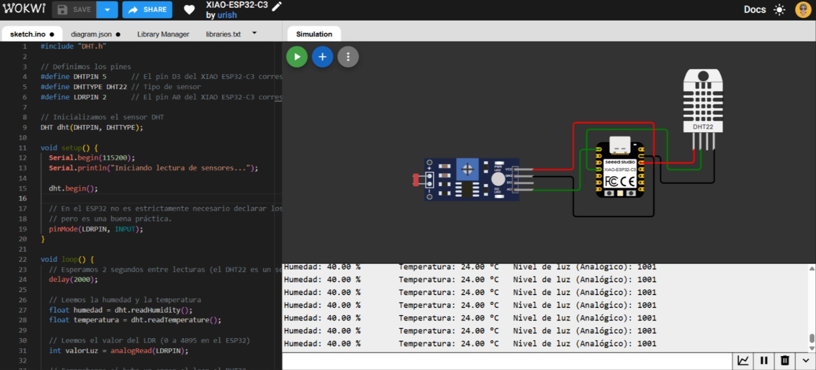
Circuit simulation in Wokwi environment.
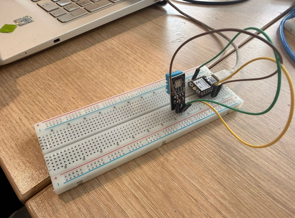
Breadboard setup with Xiao ESP32C3 and sensors.
To test the light sensor, we manually covered and uncovered the photoresistor with our hands, simulating changes in light conditions. The sensor responded by sending different values to the microcontroller, which were then displayed in the serial monitor.
For the humidity and temperature sensor, we took the setup outside the FabLab and exposed it to sunlight. This allowed us to observe real-time variations in temperature and humidity values.
This prototyping phase confirmed that both sensors were working correctly and that the code was properly interpreting the data. As a result, we gained confidence before moving on to the PCB fabrication stage.
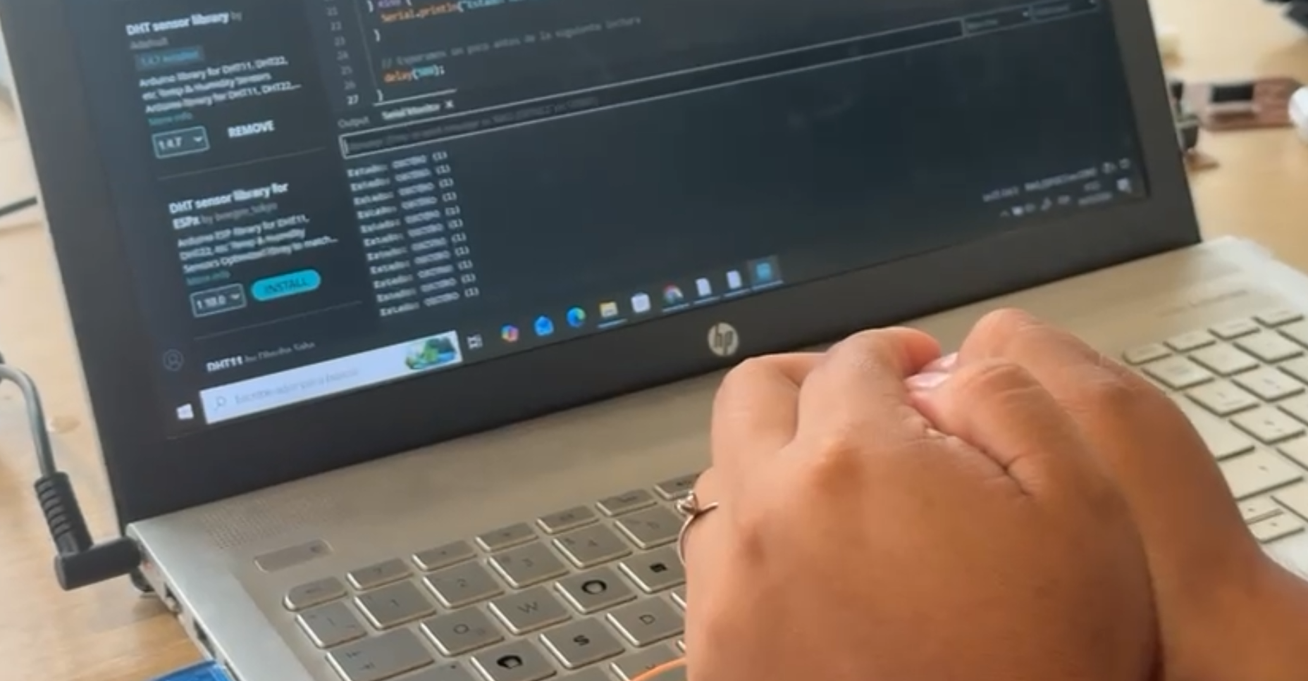
Testing light sensor by blocking light input.
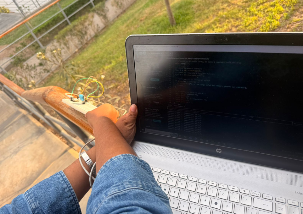
Outdoor testing of humidity and temperature sensor.
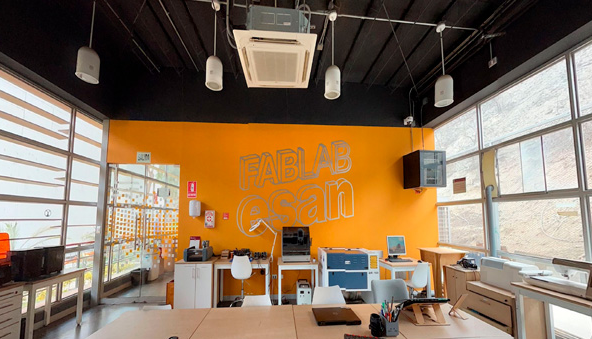
3) Fabrication Access — FabLab ESAN and PCB Design Adaptation
After defining the components and understanding the material limitations, the next step was to fabricate our PCB boards. However, we encountered a major obstacle: the PCB milling machines available in the Fab Lab Itinerante network, including the one at Fab Lab UNI, were not operational at the time.
This created a critical bottleneck in our workflow, as PCB fabrication is a required step for integrating sensors into a custom microcontroller board. Instead of stopping the process, we looked for alternative solutions and reached out to contacts within the Fab Lab network.
Through this search, we were able to connect with Jorge, who is responsible for the FabLab ESAN facility located outside the central area of Lima. Despite the distance, we decided to travel there in order to continue the fabrication process.
This decision reflects an important aspect of digital fabrication: access to machines is not always guaranteed, and problem-solving often requires logistical adaptation and collaboration.

Travel to FabLab ESAN for PCB fabrication.
Arrival and initial exploration of FabLab ESAN facilities.
3.1 Design Review with Jorge
Once we arrived at FabLab ESAN, we met with Jorge, who helped us review our PCB designs. At this stage, our initial intention was to design double-layer PCBs, which would allow more flexibility in routing.
However, Jorge explained that it was not strictly necessary to use double-layer boards. Instead, he introduced us to techniques for designing functional circuits using single-layer PCBs, which aligned with the material constraints we had already encountered.
This involved understanding how to route signals efficiently in a single layer, and how to use components such as resistors as bridges to avoid overlapping traces. This insight significantly simplified our design strategy and allowed us to move forward with fabrication.
This moment was key in our learning process, as it shifted our perspective from “ideal design” to “fabricable design”.
PCB design review and feedback session with Jorge.
3.2 Reference-Based Learning — Fab Academy Archive
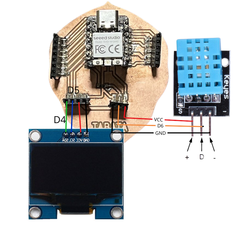
Due to our limited experience in PCB design, we decided to consult previous Fab Academy documentation to guide our process. We analyzed examples from past students and identified a particularly useful reference: a board developed by Silvana, one of our current instructors.
Her design included a microcontroller, a humidity sensor, and an OLED display, making it highly relevant to our objectives. Instead of starting entirely from scratch, we used this design as a reference to understand how components were connected and how the circuit was structured.
This approach allowed us to reverse-engineer the design, analyze routing strategies, and adapt the circuit to our own needs.
Using existing documentation as a learning resource is a fundamental principle of Fab Academy, reinforcing the importance of open knowledge sharing.
Reference PCB design used as learning base.
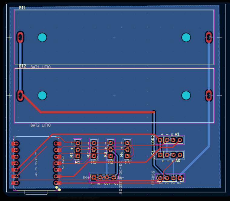
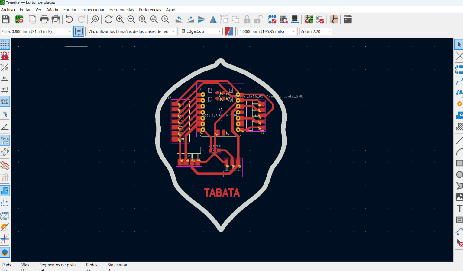
3.3 PCB Design in KiCad
After selecting the reference design, we opened the files in KiCad, which is an open-source electronic design automation (EDA) software used for schematic capture and PCB layout.
Within KiCad, we analyzed both the schematic and the PCB layout. This allowed us to understand how signals flow through the circuit and how components are physically arranged on the board.
We then adapted the design to our requirements, ensuring that it would be compatible with the components we had acquired and the single-layer PCB constraint.
Once the design was finalized, we prepared it for fabrication by exporting the necessary manufacturing files.
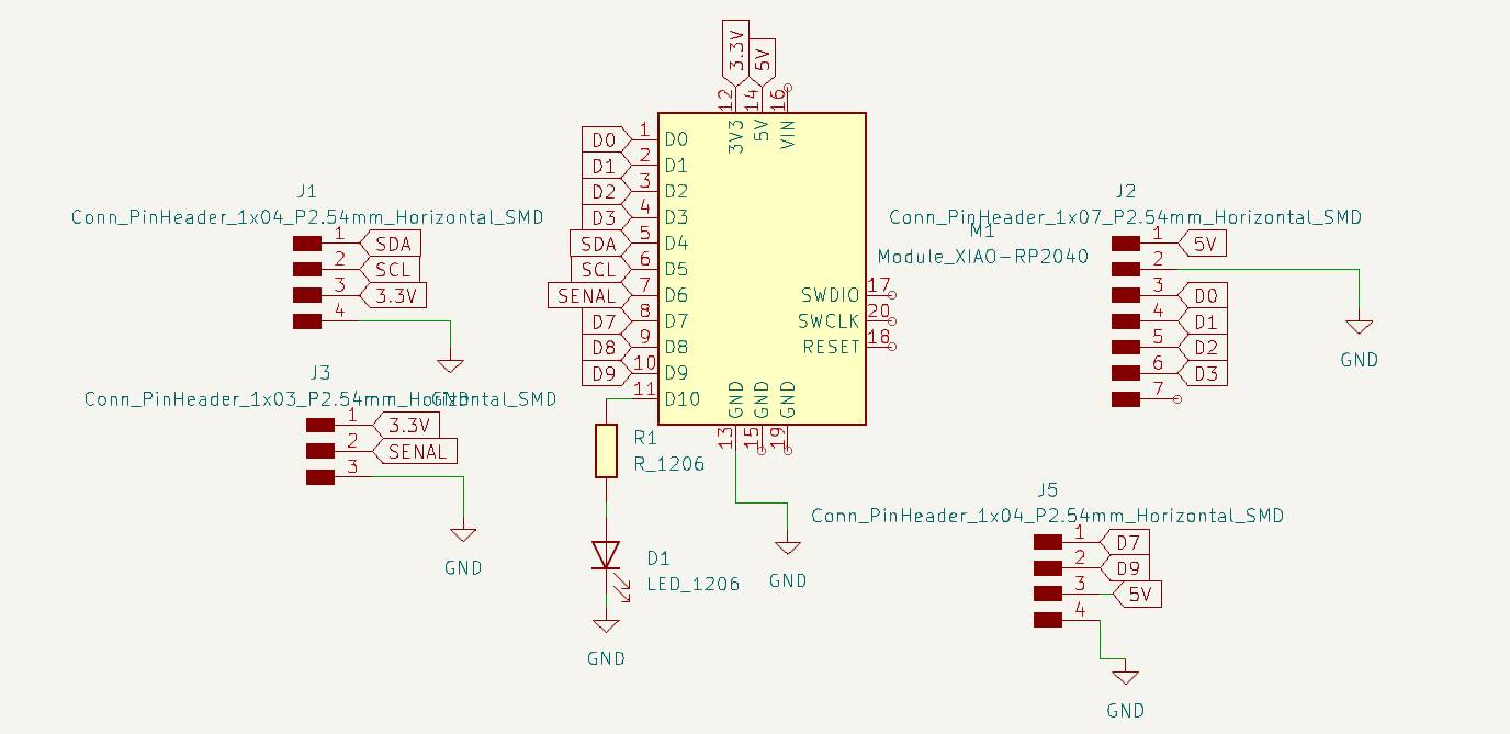
Schematic view in KiCad.
PCB layout view in KiCad.
3.4 Generating Gerber Files
To fabricate the PCB, it was necessary to generate Gerber files, which are the standard file format used in PCB manufacturing. These files contain the information required by machines to produce the traces and the board outline.
After exporting the Gerber files from KiCad, we needed to convert them into a format compatible with the CNC milling machine used at FabLab ESAN.
For this purpose, we used an online tool: Gerber2PNG
This platform allows converting Gerber files into PNG images that can be interpreted by PCB milling machines. During this process, we separated the files into two main categories:
- Traces — representing the conductive paths of the circuit
- Outline — defining the external contour of the board
This separation is essential because each operation uses a different tool and machining strategy.

Gerber to PNG conversion process.
4) PCB Fabrication — CNC Milling Process
Once the PCB design files were prepared and converted into the correct format, the next step was to fabricate the boards using a CNC milling machine available at FabLab ESAN. This process involves subtractive manufacturing, where a rotating cutting tool removes copper from the board to define the circuit traces.
Unlike industrial PCB fabrication, which uses chemical etching, CNC milling allows rapid prototyping of circuits directly within a fabrication laboratory. However, it requires careful setup, calibration, and parameter selection to ensure accurate results.
During this stage, we fabricated two PCB boards: one as an initial attempt and a second one after adjustments and improvements to the process.
PCB milling machine at FabLab ESAN.
Preparation of the copper board before machining.
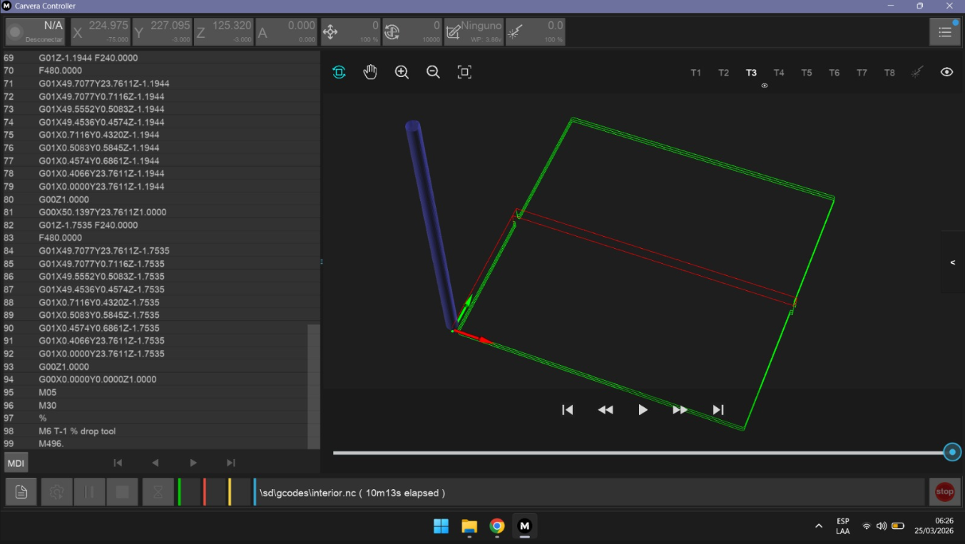
4.1 Machine Setup — Carvera Controller
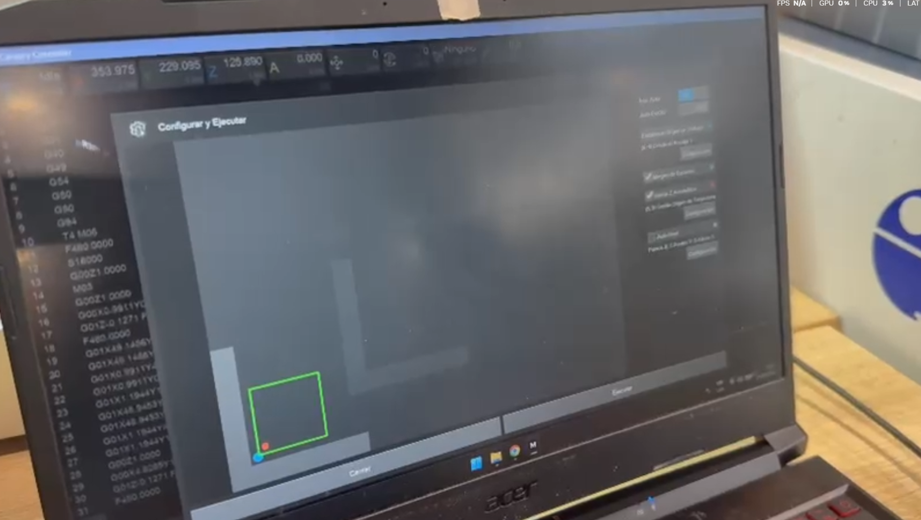
To operate the CNC milling machine, we used the software Carvera Controller, which allows communication between the computer and the milling machine.
The software was connected to the machine via USB, and from the interface we were able to load the machining files, configure tools, and control the fabrication process.
Once connected, we imported the PNG files corresponding to the traces and outline, which would be executed as separate machining operations.

Carvera Controller interface and file loading.
4.2 Tool Selection and Machining Strategy
The milling process required the use of different tools depending on the operation being performed. The machine used an automatic tool-changing system, allowing us to assign specific tools to each task.
- T4 tool — used for engraving the circuit traces
- T3 tool — used for cutting the board outline
The traces require a fine tool to accurately remove copper between conductive paths, while the outline requires a more robust tool capable of cutting through the entire thickness of the board.
Separating these processes ensures better precision and prevents damage to delicate circuit details.
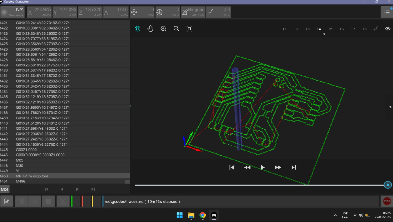
Trace engraving tool (T4).
Cutting tool for board outline (T3).
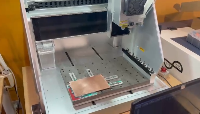
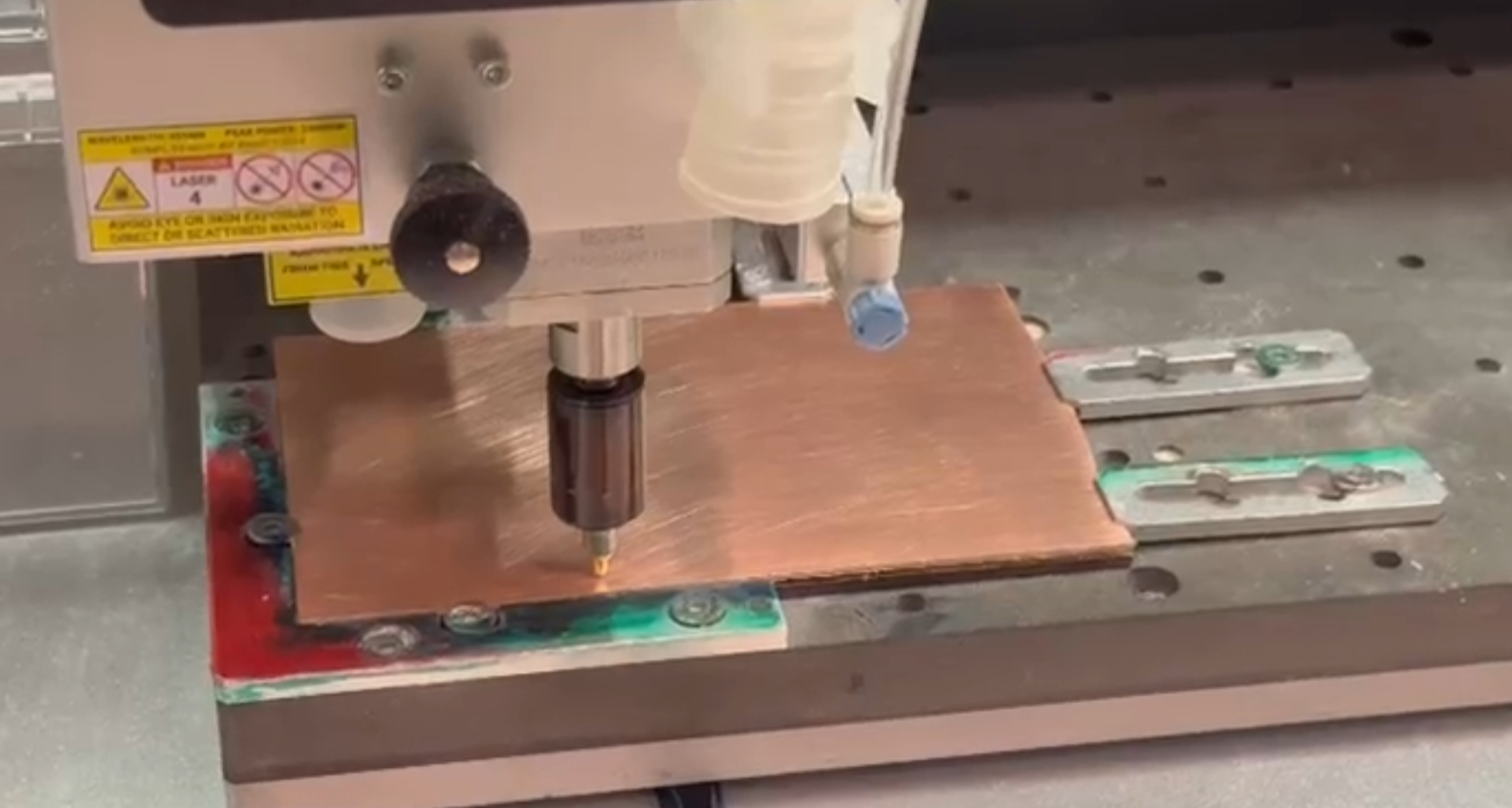
4.3 Material Fixation and Origin Setup
Before starting the machining process, the copper board (baquelita) had to be securely fixed to the machine bed. This was done using screws to prevent any movement during cutting.
The board was positioned in the lower-left corner of the working area, which was defined as the origin point (X0, Y0) of the machine.
Proper fixation is critical in PCB milling because even minimal displacement can result in misaligned traces or complete failure of the circuit.
After positioning the board, we verified the origin and prepared the machine for calibration.
Fixing the PCB material and setting origin point.
4.4 Auto Calibration and Milling Process
Before starting the cutting process, the machine performed an auto-calibration routine. This step ensures that the tool height is correctly adjusted relative to the surface of the material.
We configured the machine to perform a 5-point calibration, allowing it to detect variations in the surface level of the board. This is especially important because slight irregularities in the material can affect cutting depth and trace quality.
Once calibration was complete, the machine began executing the toolpath for the traces using the T4 tool. The milling bit moved across the board, removing copper to define the circuit paths.
After completing the traces, the second operation was executed using the T3 tool to cut the outer contour of the board.
Auto-calibration process.
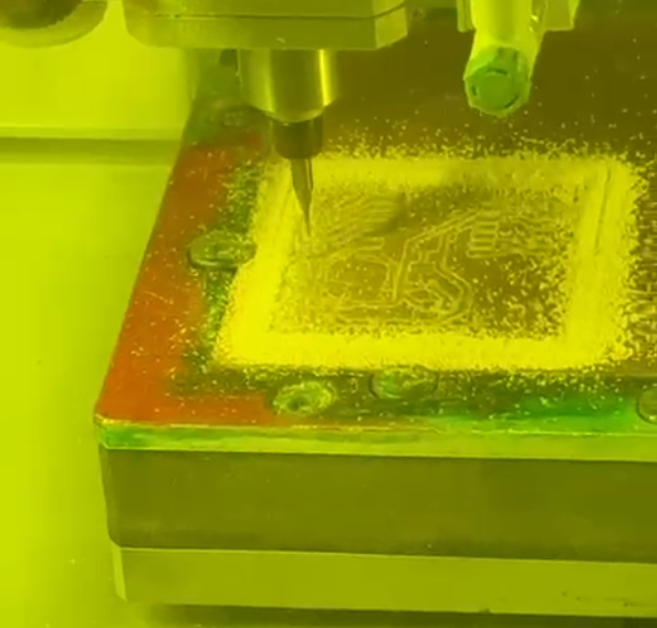
PCB traces milling process.
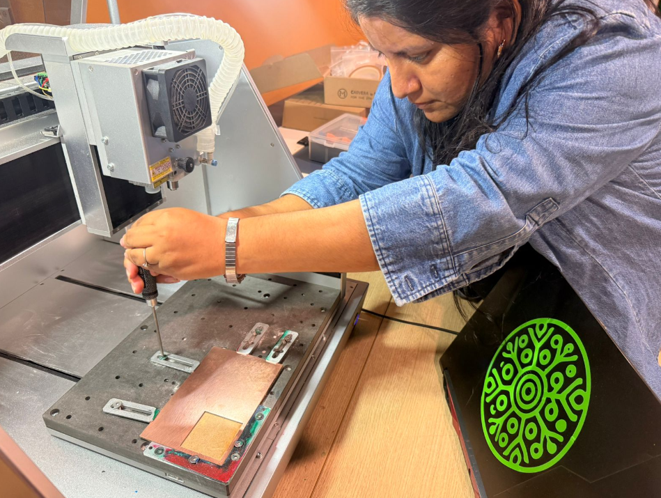
4.5 Board Cutting and Finishing
During the outline cutting process, small tabs were intentionally left connecting the board to the base material. These tabs prevent the board from detaching prematurely and moving during machining.
After the milling process was completed, we cleaned the surface using a vacuum to remove copper debris. Then, we manually cut the tabs using a small hand saw to release the PCB from the board.
This resulted in two fabricated PCB boards, one of which would later be used for testing and soldering.
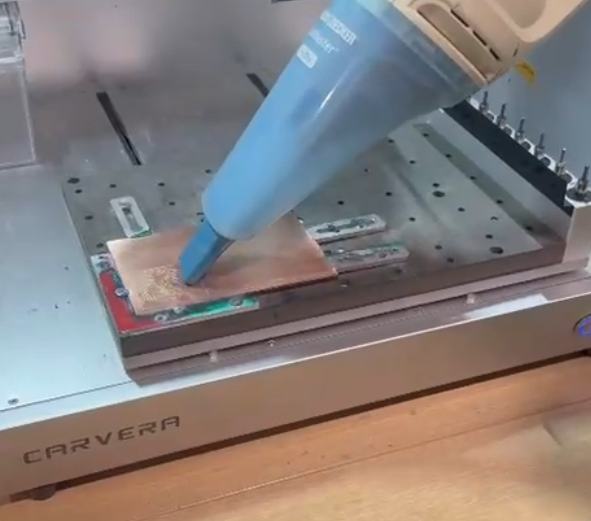
Cleaning debris after milling.
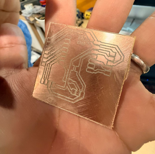
Final PCB boards after cutting.
5) Assembly, Debugging and Final Result
After completing the PCB fabrication process, the next step was to assemble the electronic components onto the board and test whether the system was capable of reading sensor data correctly. This stage introduced a completely new set of challenges, as it involved soldering, programming, and debugging.
Since the FabLab facilities were closing, we needed to find an alternative space to continue working. With the support of Carmen, we relocated to her brother’s apartment, where we set up a temporary workspace to complete the soldering and testing process.
This situation reflects a common reality in digital fabrication workflows: the ability to adapt and continue working outside of ideal laboratory conditions.
Temporary workspace for soldering process.
Preparing tools and components for assembly.
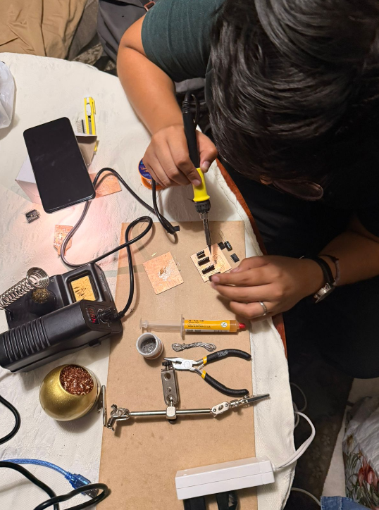
5.1 First Soldering Attempt — Learning Phase
Since this was our first experience soldering electronic components, we decided to use the PCB that had lower fabrication quality as a test board. This allowed us to practice soldering techniques without risking the better-fabricated board.
Using a soldering iron and tin wire, we carefully attached the microcontroller, sensor components, and connectors. During this process, we learned how to control heat, apply solder properly, and avoid short circuits between pins.
However, once the assembly was completed and we uploaded the code, the system did not behave as expected.
Initial soldering attempt on test PCB.
5.2 Debugging — Code and Hardware Issues
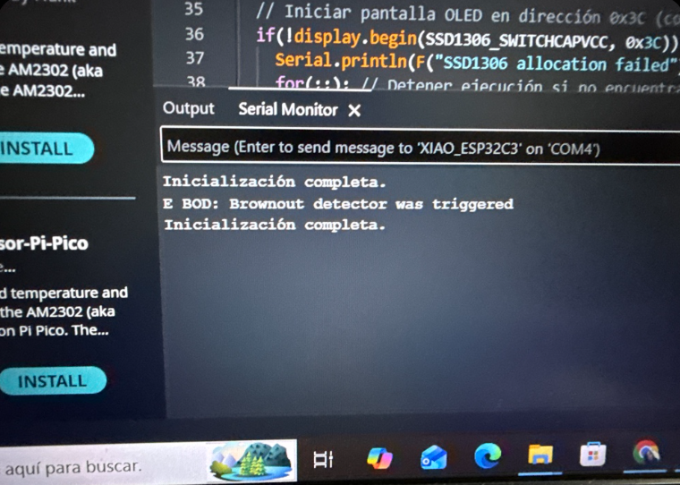
After uploading the program to the microcontroller, the system initialized correctly, but no sensor data was being received. The OLED display turned on, indicating that the board had power, but the readings remained empty.
To troubleshoot the issue, we analyzed both the code and the hardware connections. Using tools such as ChatGPT and Google Gemini, we reviewed the code structure and corrected several inconsistencies.
Despite these corrections, the problem persisted. At this point, the debugging process shifted toward hardware analysis.
One of the key error messages we encountered was a Brownout error, which typically indicates an issue with power supply or voltage instability in the circuit.
This suggested that the problem might not be related to the code, but rather to the physical PCB or its connections.
Error messages observed during debugging process.
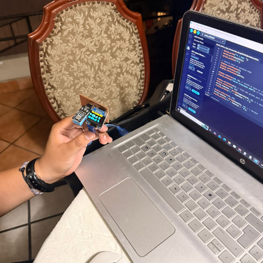
5.3 Hypothesis Testing — Jumper Wire Validation
Based on the error analysis, we hypothesized that the PCB might have a faulty connection, particularly in the power distribution from the microcontroller to the sensors.
To test this hypothesis, we bypassed the PCB connections using jumper wires. We directly connected the sensor to the microcontroller pins, ensuring proper voltage and signal routing.
Once this setup was completed, we uploaded the same code again.
This time, the system successfully read the sensor data, confirming that the issue was indeed related to the PCB and not the code or sensor.

Testing circuit using jumper wires.
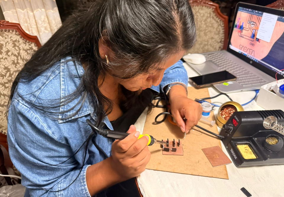
5.4 Second PCB Assembly — Successful Integration
After confirming that the problem was caused by the first PCB, we proceeded to assemble the second board, which had better fabrication quality.
With the experience gained from the first attempt, the soldering process was significantly more precise. We focused on ensuring clean joints and avoiding any possible short circuits.
We then connected the microcontroller and uploaded the corrected code.
This time, the system worked correctly, and the sensor data was successfully received and processed.
Final PCB assembly with improved soldering.
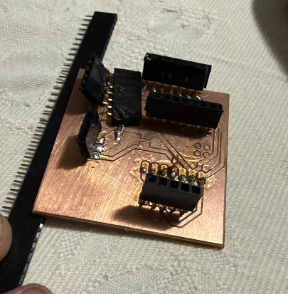
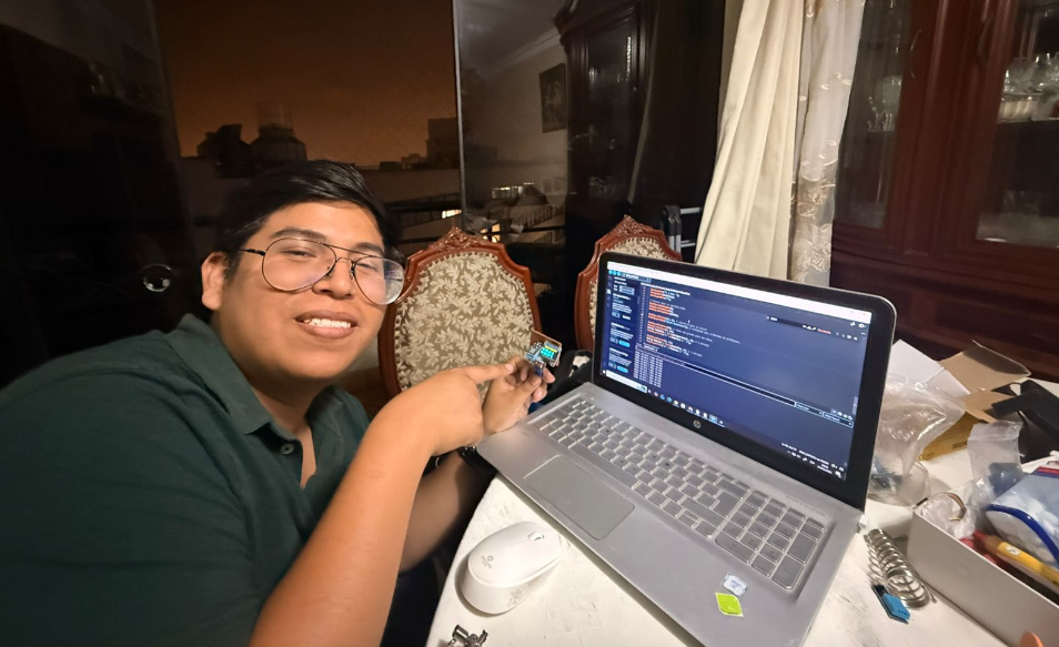
5.5 Final Result — Sensor Data Acquisition
The final system successfully measured environmental data using the sensor integrated into the custom PCB. The readings were displayed in the serial monitor and also visualized through the OLED display.
To validate the functionality, we tested the sensor in different environmental conditions. For example, the humidity and temperature sensor was exposed to sunlight, allowing us to observe real-time variations in the data.
Similarly, the light sensor was tested by covering and uncovering it, simulating changes in light exposure.
These tests confirmed that the system was capable of measuring physical variables and translating them into digital data.
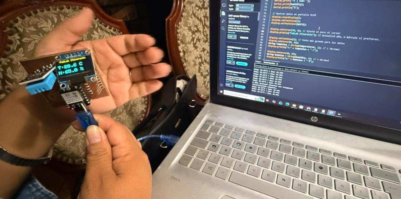
Sensor data displayed in serial monitor.
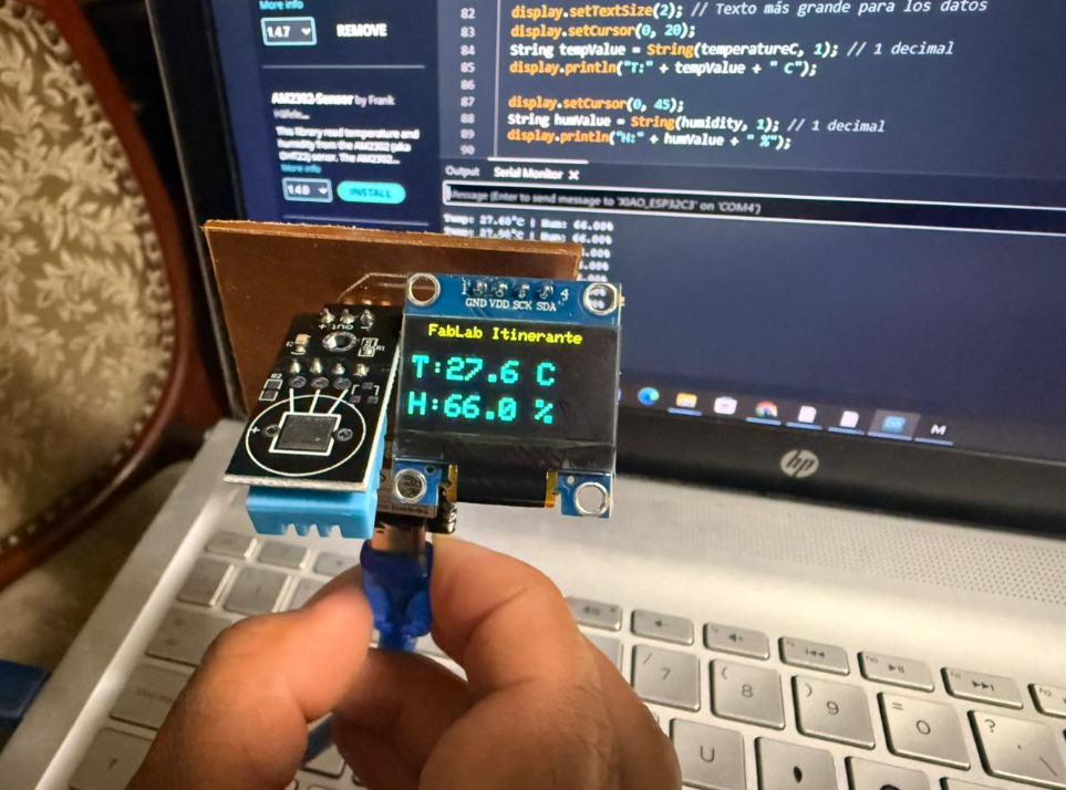
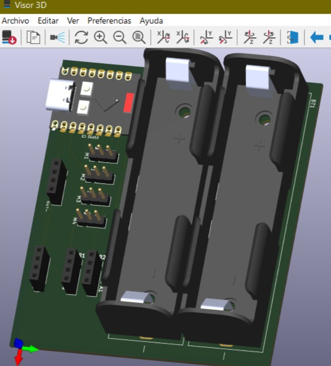
Final PCB with OLED display and sensor working.
5.6 Final Documentation and Closing
After successfully completing the system, we documented the final results, including the working PCB, sensor outputs, and the overall process.
This assignment not only allowed us to understand how input devices work, but also highlighted the importance of iterative design, debugging, and collaborative problem-solving in digital fabrication.
Final result with Jorge and completed PCB.
6) Reflection
This week represented one of the most challenging yet rewarding experiences of the Fab Academy so far. It required integrating knowledge from electronics design, fabrication, programming, and debugging into a single workflow.
One of the most important lessons was understanding that failures are an essential part of the process. The first PCB did not work, but it provided valuable insights that allowed us to improve and succeed with the second attempt.
Another key takeaway was the importance of systematic debugging. By isolating variables and testing hypotheses step by step, we were able to identify the root cause of the problem.
Additionally, this experience reinforced the value of collaboration. Working alongside Carmen allowed us to share knowledge, support each other, and solve complex problems more efficiently.
Overall, this week helped me understand how to transform a conceptual electronic system into a fully functional physical device capable of measuring real-world data.
7) Files
The following files correspond to the electronic design, code, and fabrication resources developed during Week 09. These files document the complete workflow from simulation and PCB design to fabrication and testing of the input device system.
- PCB Design (KiCad Files) Download KiCad File
- Schematic Diagram Download PDF
- Gerber Files Download Gerber Package
- PNG Files for Milling Download Traces PNG
- Download Outline PNG
- Arduino Code (Sensor Reading) Download .INO File
- Wokwi Simulation File Download Simulation
All files are provided for documentation and educational purposes as part of the Fab Academy program. They represent the full development cycle of an input device system, including design, fabrication, and debugging.