
Assignment Requirements
Group assignment
- Use the test equipment in your lab to observe the operation of a microcontroller circuit board (as a minimum, you should demonstrate the use of a logic analyzer)
- Document your work on the group work page and reflect what you learned on your individual page
Individual assignment
- Simulate a circuit
- Use an EDA tool to design an embedded microcontroller system using parts from the inventory, and check its design rules for fabrication
- extra credit: try another design workflow
- extra credit: design a case
Progress Status
Laboratory measurements and signal observation
EDA design of development board
Uploading source design files
1) Group Assignment — Distributed Testing Electronics (Fab Itinerante)
This week introduced us to the practical side of electronics testing. Instead of only programming microcontrollers, we learned how to analyze their electrical behavior using professional laboratory instruments.
In our Fab Academy cohort we work under the distributed fabrication model known as Fab Itinerante. Because of this, assignments are often carried out across different laboratories and workspaces while documentation and collaboration happen digitally.
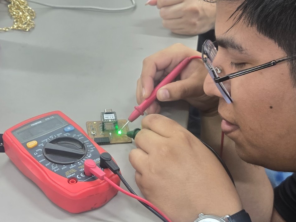
For this week we met at Fab Lab UNI, where we had access to professional electronic measurement tools such as a digital multimeter and a digital oscilloscope. Using these tools we were able to observe the digital signals produced by a microcontroller and verify that the board was operating correctly.
2) Distributed Fabrication Context — Fab Itinerante
The group assignment for this week focused on analyzing the behavior of a microcontroller circuit using laboratory measurement equipment. Similar to previous weeks in the Fab Academy program, this exercise was carried out under the Fab Itinerante distributed fabrication model.
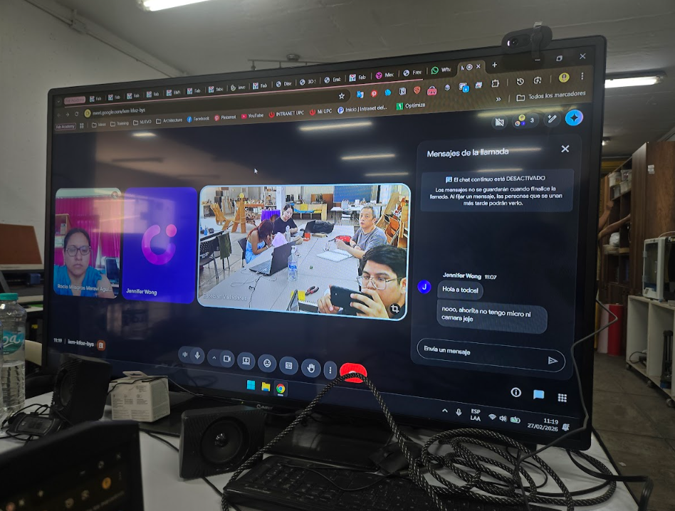
Rather than working from a single laboratory, participants conducted the experiments from different Fab Labs across Peru while maintaining coordinated documentation and collaboration. This decentralized approach reflects the core philosophy of the Fab Lab network: local experimentation combined with shared digital knowledge and standardized documentation.
Distributed Laboratory Context
During this assignment, our group operated from several Fab Labs simultaneously:
- Carmen, with the support of instructor Mauro, worked from Fab Lab Koajika Satipo in Satipo, located in the Peruvian Amazon.
- David, Esteban, Jean Franco, Cindy, Grace, and Mario carried out the experiments at Fab Lab UNI in Lima.
- Rocío participated from her local laboratory in Fab Lab Madre de Dios, also located in the Amazon region.
- Jennifer joined the group remotely from the Fab Lab at Universidad del Pacífico in Lima.
Although our group was geographically distributed, the experiments were coordinated collectively so that all participants could understand and replicate the same measurement process.
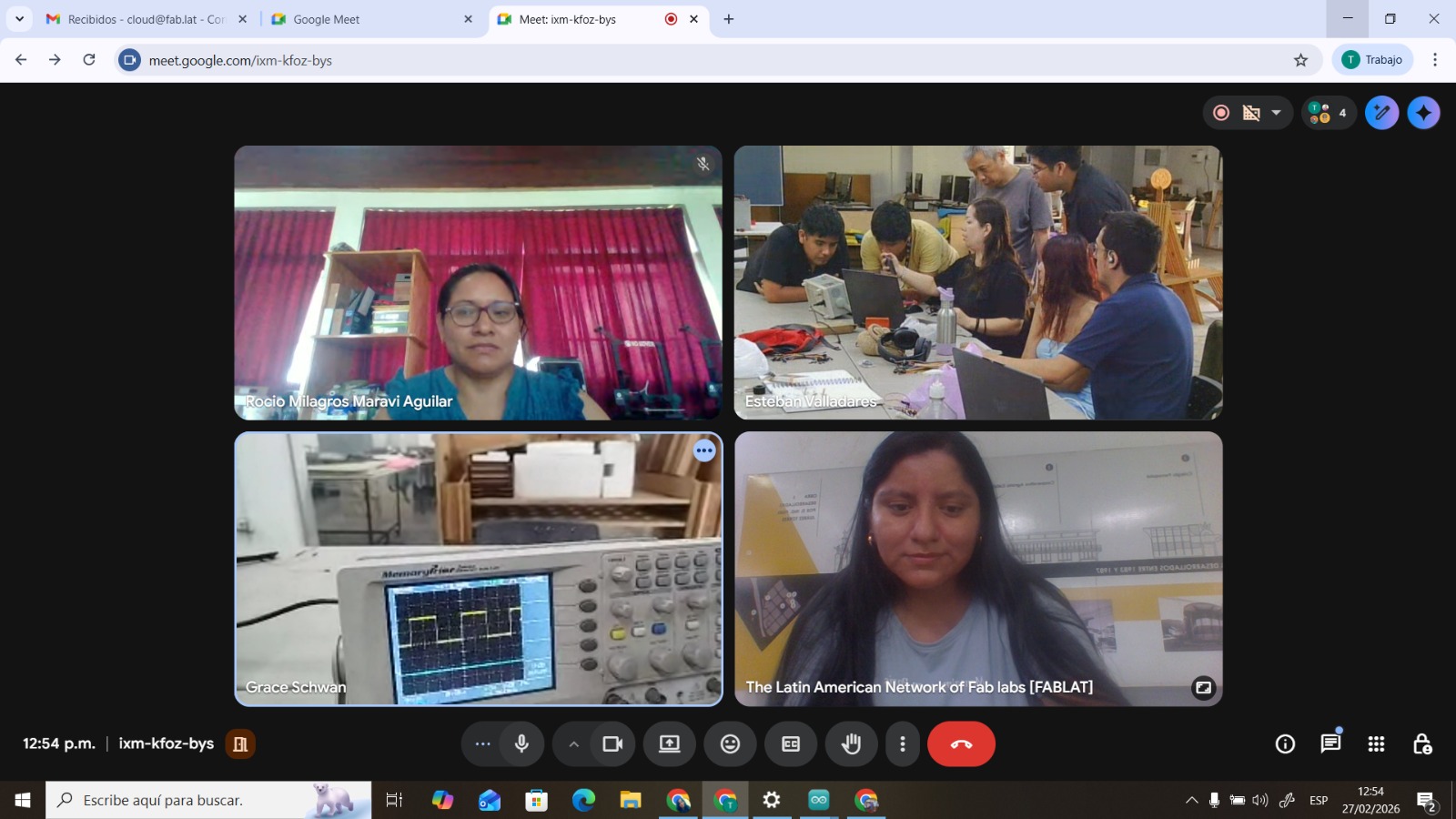
Fab Academy students collaborating from different Fab Labs across Peru.
Experiment Coordination
The main group located at Fab Lab UNI performed the experimental measurements using the available laboratory equipment. These tests included voltage verification with a digital multimeter and signal visualization with a digital oscilloscope.
Meanwhile, the teams located in other Fab Labs followed the same procedure remotely and attempted to replicate the experiment using their available tools and equipment. Communication between teams allowed everyone to observe the methodology and understand the measurement workflow.
By coordinating the experiment across different laboratories, we were able to ensure that the measurement process could be reproduced in different contexts, reinforcing the distributed learning model that characterizes the Fab Academy program.
3) Equipment and Materials
To analyze the behavior of the microcontroller circuit we used two fundamental electronic measurement instruments: a digital multimeter and a digital oscilloscope. Each device serves a different purpose when diagnosing or analyzing electronic systems.
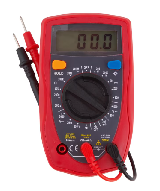
Digital Multimeter – PR-75
The PR-75 is a handheld digital multimeter designed for general electrical and electronic measurements. Multimeters are commonly used for diagnosing circuits, checking voltage levels, and verifying electrical continuity.
Main capabilities:
- DC voltage measurement up to 600V
- AC voltage measurement
- Resistance measurement (Ω)
- Continuity testing with buzzer
- Diode testing
- Current measurement (mA and 10A)
In our experiment the multimeter was used to verify that the microcontroller board was receiving the correct voltage supply (3.3V) and to ensure that no short circuits were present before connecting the oscilloscope.
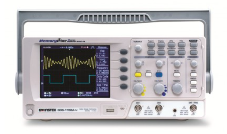
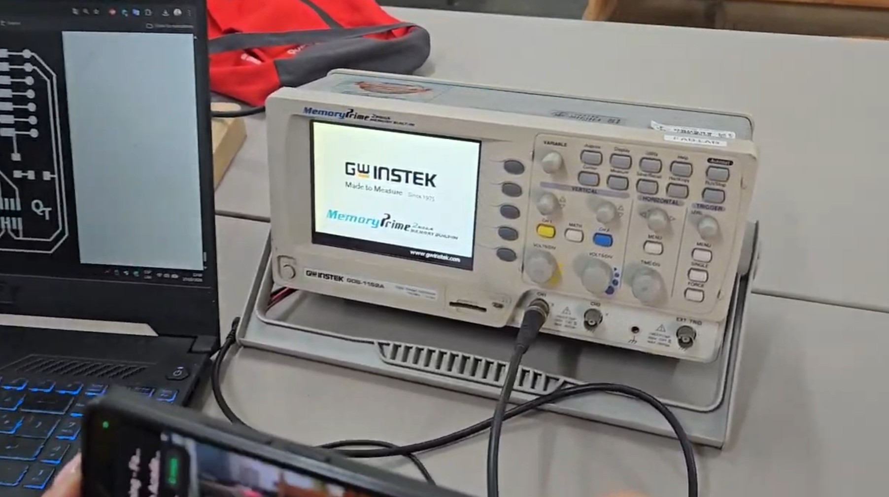
Digital Oscilloscope – GW Instek GDS-1152A
An oscilloscope is an electronic instrument used to visualize electrical signals as waveforms over time. Unlike a multimeter, which only provides numerical values, the oscilloscope allows us to observe how signals evolve dynamically.
Main specifications:
- Bandwidth: 150 MHz
- 2 independent channels (CH1 / CH2)
- Digital storage oscilloscope (DSO)
- AutoSet automatic signal detection
- Adjustable VOLTS/DIV and TIME/DIV
- Trigger system for signal stabilization
In this assignment the oscilloscope allowed us to visualize the square wave generated by the microcontroller GPIO pin, confirming that the digital output signal was functioning correctly.
4) Technical Comparison of Measurement Instruments
Although both the multimeter and the oscilloscope measure electrical signals, they provide different types of information. Understanding when to use each instrument is fundamental for electronics debugging and circuit validation.
| Instrument | Primary Function | Measurements | Use in Experiment |
|---|---|---|---|
| Digital Multimeter | Direct electrical measurement | Voltage, resistance, current, continuity | Verify power supply and detect short circuits |
| Oscilloscope | Signal visualization over time | Waveform shape, frequency, voltage levels | Observe square wave produced by GPIO pin |
In simple terms, the multimeter answers the question "what is the voltage?", while the oscilloscope answers "how does the voltage change over time?".
5) Microcontroller Board Tested
For the signal analysis we used a custom microcontroller board based on the Seeed Studio XIAO RP2040. This board uses the Raspberry Pi RP2040 microcontroller, which is a dual-core ARM Cortex-M0+ processor designed for embedded applications.
| Feature | Specification |
|---|---|
| Microcontroller | RP2040 |
| CPU Architecture | Dual-core ARM Cortex-M0+ |
| Clock Speed | Up to 133 MHz |
| SRAM | 264 KB |
| Flash Memory | External SPI Flash |
| Operating Voltage | 3.3V |
| GPIO | Multiple programmable digital pins |
For the purpose of this experiment, the microcontroller was programmed to generate a digital square wave through one of its GPIO pins.
6) Experimental Procedure
To observe the behavior of the microcontroller circuit, we followed a step-by-step measurement procedure combining both instruments.
Step 1 — Power Verification
The first step was verifying that the microcontroller board was receiving the correct voltage supply.
- Multimeter set to DC voltage mode
- Black probe connected to GND
- Red probe connected to VCC
- Measured value ≈ 3.3V
This confirmed that the board was correctly powered and safe for further testing.
Step 2 — Oscilloscope Connection
After confirming the power supply, the oscilloscope probe was connected to the digital output pin of the microcontroller.
- Ground clip connected to board GND
- Probe tip connected to GPIO output pin
Oscilloscope configuration used:
- Channel: CH1
- Voltage scale: 1V/div
- Time scale: 1ms/div
- Trigger mode: Edge
- AutoSet for initial calibration
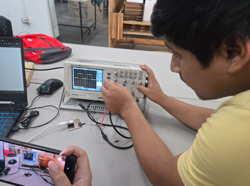
Step 3 — Signal Observation
After uploading the program to the microcontroller, the GPIO pin started generating a digital signal.
The oscilloscope displayed a clear square waveform, showing the transition between digital LOW and HIGH states.
- LOW state ≈ 0V
- HIGH state ≈ 3.3V
- Stable signal frequency
This confirmed that the microcontroller was executing the program correctly and that the digital output was functioning as expected.
7) Results — Digital Signal Observation
After configuring the instruments and uploading the program to the microcontroller board, we were able to observe the digital signal generated by the GPIO output pin using the oscilloscope.
The signal displayed on the oscilloscope corresponded to a typical square wave, which represents the alternating digital states between HIGH and LOW used in microcontroller programming.
| Parameter | Expected Value | Observed Value | Status |
|---|---|---|---|
| Supply Voltage | 3.3V | ≈ 3.3V | Stable |
| Digital LOW | 0V | ≈ 0V | Correct |
| Digital HIGH | 3.3V | ≈ 3.3V | Correct |
| Signal Type | Square Wave | Square Wave | Verified |
These measurements confirmed that the microcontroller was executing the program correctly and that the digital output pin was switching between logic states as expected.
8) Signal Analysis
The oscilloscope visualization allowed us to observe how digital signals behave physically inside electronic systems. Unlike software simulations, real hardware signals can be affected by timing, voltage stability, and electrical noise.
In this experiment the waveform observed was a stable square signal oscillating between approximately 0V and 3.3V, which corresponds to the logical LOW and HIGH states of the microcontroller.
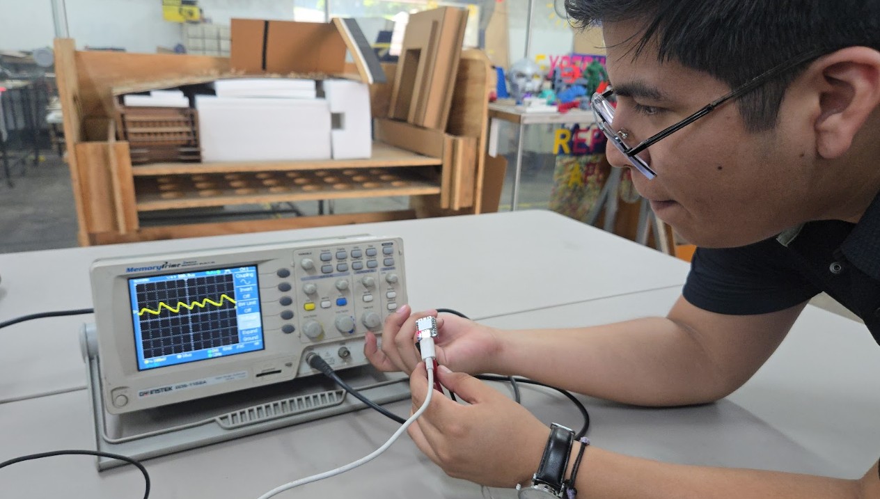
Oscilloscope displaying the square wave generated by the microcontroller.
Digital signal transitions between LOW and HIGH states.
Being able to visualize this waveform helps engineers verify that a microcontroller is operating correctly and that its internal clock and digital output systems are functioning as intended.
9) Learning Outcomes
This exercise introduced several fundamental concepts related to electronics measurement and embedded system debugging.
- Understanding the difference between measuring voltage and visualizing signals
- Learning how to safely connect measurement instruments to electronic circuits
- Observing real digital signals produced by a microcontroller
- Understanding the importance of grounding when measuring electronic systems
- Learning how oscilloscopes visualize time-based signals
These concepts are essential for diagnosing electronic circuits and verifying the correct operation of embedded systems.
10) Reflection
For someone coming from an architectural background, this week represented an important step in understanding the physical layer behind digital systems. While programming microcontrollers allows us to control behavior logically, using laboratory measurement tools reveals how those instructions translate into electrical signals in real hardware.
Seeing the square wave produced by the microcontroller helped me understand that behind every digital instruction there is a physical voltage transition happening inside the circuit.
In architecture we often think in terms of spatial systems, structural logic, and environmental flows. In electronics, signals behave almost like dynamic flows of energy that travel through circuits following precise timing rules.
Learning to observe and analyze these signals is essential for designing reliable embedded systems, especially when working with responsive architectural environments and interactive installations.
11) References
- GW Instek GDS-1152A Oscilloscope Documentation https://www.gwinstek.com
- Basic Oscilloscope Operation Guide https://learn.sparkfun.com/tutorials/how-to-use-an-oscilloscope
- Seeed Studio XIAO RP2040 Documentation https://wiki.seeedstudio.com/XIAO-RP2040/
12) Individual Assignment — Electronics Design
The objective of this week was to design an electronic development board using an EDA (Electronic Design Automation) tool capable of interacting with an embedded microcontroller.
Rather than designing an arbitrary electronic board, I decided to use this assignment as an opportunity to develop the electronic foundation of my final project. My final project explores adaptive architectural systems capable of responding to environmental conditions such as solar radiation.
12.1 Translating an Architectural Idea into an Electronic System
Coming from an architecture background, understanding electronics required translating technical concepts into spatial and systemic thinking. Instead of starting with components, I first needed to understand how responsive architectural systems are structured.
Many kinetic systems developed in Fab Academy and in responsive architecture follow a similar logical structure:
SENSOR → MICROCONTROLLER → MOTOR DRIVER → MOTOR → MECHANISM
This chain allows environmental information to be captured, processed, and transformed into physical movement.
For example, a typical responsive façade might detect sunlight intensity, calculate the desired shading level, and adjust mechanical panels accordingly.
General architecture of responsive kinetic systems used in Fab Academy projects.
12.2 Translating My Final Project into an Electronic Architecture
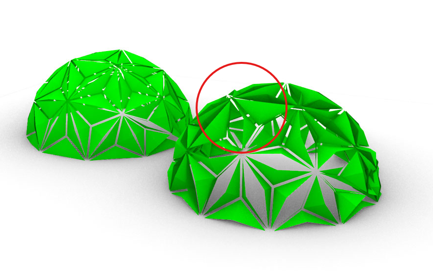
My final project explores a modular dome structure composed of triangular elements that can open and close depending on solar radiation conditions.
To translate this idea into an embedded system, I mapped the architectural behavior into an electronic logic:
SUNLIGHT
↓
LIGHT SENSOR
↓
MICROCONTROLLER
↓
MOTOR DRIVER
↓
STEPPER MOTOR
↓
KINETIC JOINT
↓
GEOMETRIC DOME OPENING
This process helped me understand that architecture, electronics, and computation can be interpreted as different layers of the same responsive system.
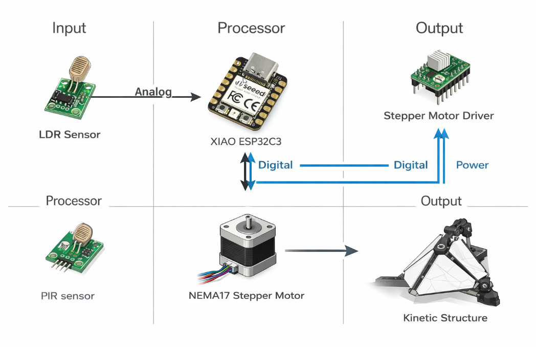
12.3 System Definition Using the Input / Processor / Output Model
To structure the system more clearly, I defined it using the classical embedded systems model: Input → Processor → Output.
| Layer | Component | Function |
|---|---|---|
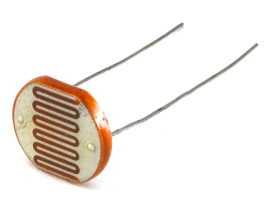
| INPUT | Photoresistor (LDR) | Measures environmental light intensity |
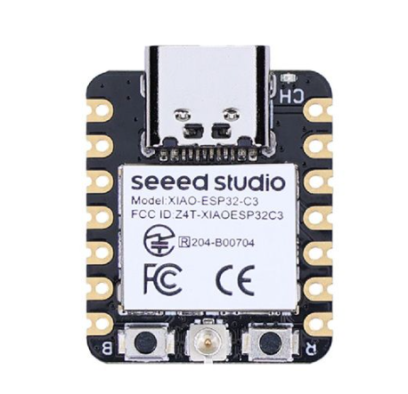
| PROCESSOR | Seeed Studio XIAO ESP32C3 | Processes sensor data and determines system response |
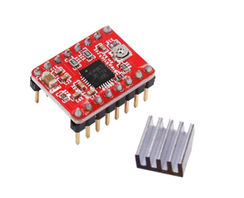
| OUTPUT | Stepper motor driver (A4988) | Controls motor movement |
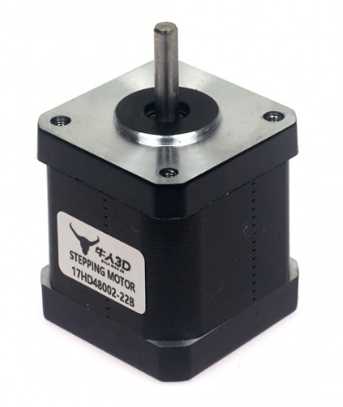
| ACTUATOR | NEMA17 Stepper Motor | Generates mechanical motion |
| MECHANISM | Kinetic architectural joint | Transforms motor rotation into geometric movement |
This simple structure provided a clear roadmap for how the electronics, software, and mechanical systems will interact in the final prototype.
12.4 Selecting the Components
Another important step was selecting components that are realistic to obtain locally. Because Fab Itinerante does not currently have a complete electronics inventory, many components must be sourced individually.
In Lima, the most common place to buy electronic components is the Paruro electronics market.
| Component | Purpose | Availability |
|---|---|---|
| LDR Photoresistor | Light sensing | Paruro market |
| XIAO ESP32C3 | Microcontroller | Imported / limited stock |
| A4988 Driver | Stepper motor control | Paruro market |
| NEMA17 Stepper Motor | Mechanical motion | Common in robotics stores |
| Resistors / Capacitors | Electronic stability | Widely available |
This selection ensured that the system is not only theoretically possible, but also realistically buildable using locally accessible components.
12.5 How the System Will Behave
At the software level, the system will operate by reading the light intensity and translating that value into a structural opening percentage.
light_value = analogRead(sensor)

opening = map(light_value, 0,1024,0,100)

if opening > current_position
    open_structure()

if opening < current_position
    close_structure()
This logic allows the kinetic module to gradually respond to environmental changes. Small fluctuations in light are filtered so the system does not oscillate constantly.
12.6 Mechanical Translation of the System
The electronic signals will eventually control a mechanical mechanism that transforms rotational motion into geometric transformation.
Stepper motor
↓
Lead screw
↓
Linear slider
↓
Hinge joint
↓
Triangular panel
When the slider moves upward, the triangular panels open. When it moves downward, the panels close.
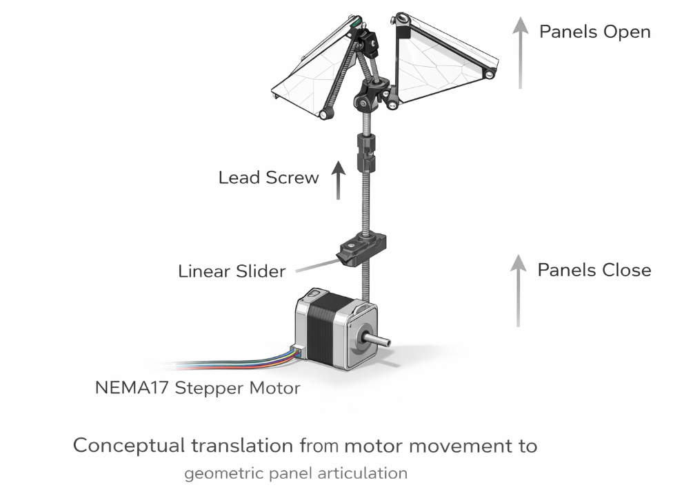
Conceptual translation from motor movement to geometric panel articulation.
12.7 Prototyping Strategy
Instead of attempting to build a full dome immediately, the project will evolve through progressive prototyping stages:
| Stage | Description |
|---|---|
| Stage 1 | Single panel kinetic prototype |
| Stage 2 | Three panel articulation |
| Stage 3 | Full hexagonal module |
| Stage 4 | Parametric dome assembly |
The electronics designed this week will act as the control layer for these future prototypes.
12.8 Electronic Design Workflow
After defining the system architecture of the project, the next step was translating this conceptual structure into an actual electronic circuit that could later be fabricated as a PCB (Printed Circuit Board).
To achieve this, I followed the standard electronic design workflow used in embedded systems development and digital fabrication environments.
System concept
↓
Electronic architecture
↓
Hand sketch diagram
↓
Schematic design (KiCad)
↓
Footprint assignment
↓
PCB layout
↓
Routing
↓
Design Rule Check (DRC)
↓
Gerber export
↓
CAM processing (FlatCAM)
This workflow transforms an idea into a manufacturable electronic board.
12.9 What is an EDA Tool?
EDA stands for Electronic Design Automation. These are specialized software platforms used to design electronic circuits, schematics, and printed circuit boards.
EDA tools allow designers to define electrical connections, simulate circuits, and generate the manufacturing files needed to fabricate PCBs.
| Software | Use | Type |
|---|---|---|
| KiCad | PCB and schematic design | Open source |
| Eagle | PCB design | Commercial |
| Altium | Professional electronics design | Industrial |
| EasyEDA | Online circuit design | Web-based |
In Fab Academy we primarily use KiCad because it is open source, powerful, and compatible with digital fabrication workflows.
Official website: https://www.kicad.org
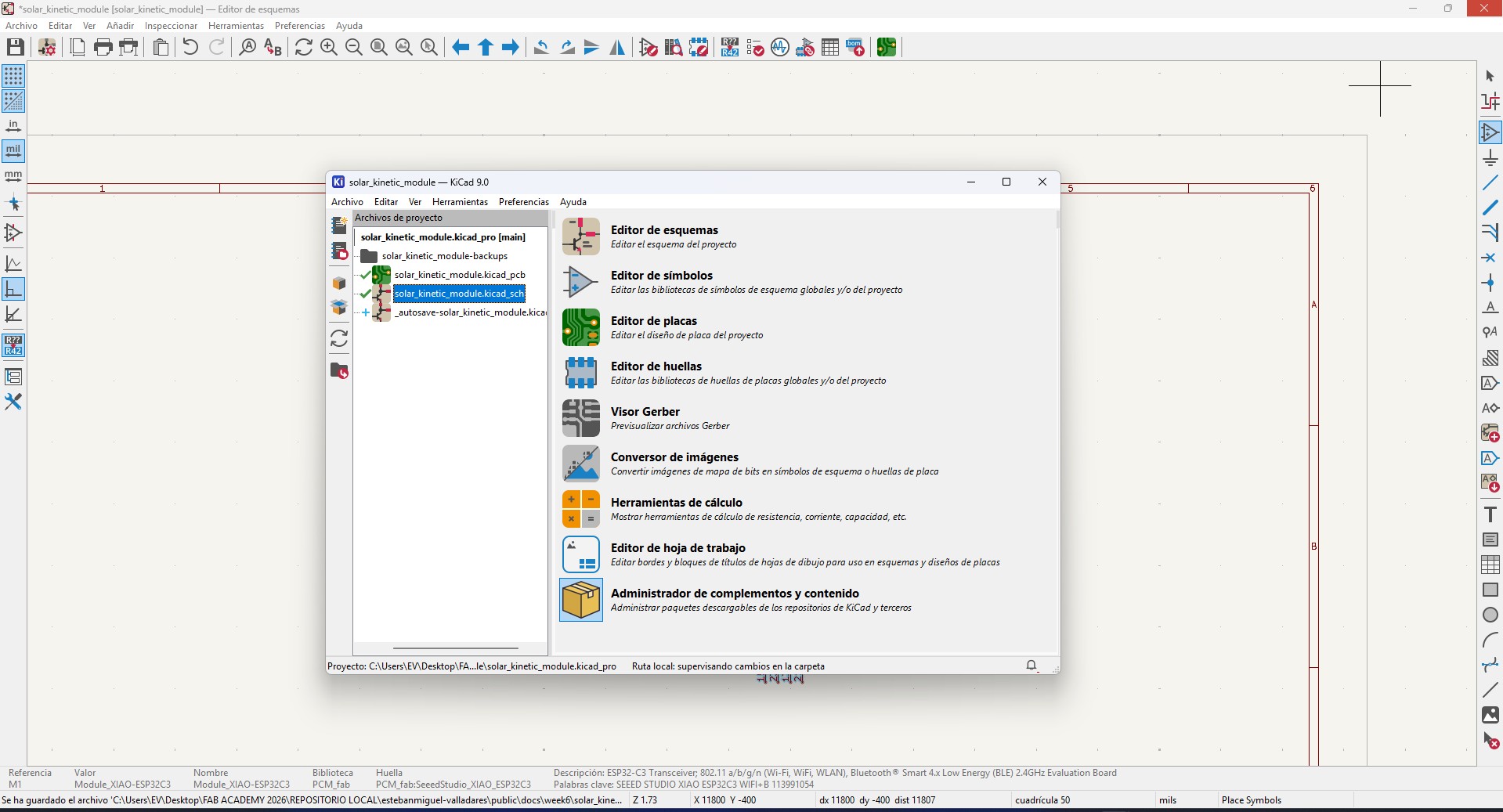
KiCad interface used for schematic capture and PCB layout.
12.10 Defining the Electronic System
Before opening KiCad, it is essential to define the electronic system that the board will support.
Following the Input / Processor / Output structure, the electronic architecture for my project was defined as follows:
| System Layer | Component | Description |
|---|---|---|
| Input | LDR Light Sensor | Measures environmental light intensity |
| Processor | XIAO ESP32C3 | Processes sensor data and executes control logic |
| Output | A4988 Stepper Driver | Translates digital signals into motor current |
| Actuator | NEMA17 Stepper Motor | Produces mechanical movement |
LDR Light Sensor
XIAO ESP32C3
A4988 Stepper Driver
NEMA17 Stepper Motor
However, during this week's assignment the focus was on designing the microcontroller board and the sensor interface. The motor driver will be connected later through header pins.
12.11 Hand Sketch of the Circuit
Before designing the schematic digitally, it is good practice to draw the circuit manually. This helps visualize the electrical relationships between components.
In this case, the basic sensing circuit is a voltage divider that allows the microcontroller to measure light intensity.
3.3V
 |
LDR
 |
Signal → Analog Pin
 |
10k Resistor
 |
GND
This configuration converts resistance changes in the photoresistor into voltage changes that can be measured by the microcontroller's analog-to-digital converter.
6.12 Voltage Divider Principle
The voltage divider is one of the most common circuits used for analog sensing.
A voltage divider uses two resistive elements to generate a fraction of the supply voltage.
Vout = Vin * (R2 / (R1 + R2))
In this project:
- R1 = fixed resistor (10kΩ)
- R2 = LDR photoresistor
- Vin = 3.3V supply from the XIAO ESP32C3
When the light intensity changes, the resistance of the LDR changes, which modifies the output voltage measured by the microcontroller.
12.13 Preparing the Schematic Design
Once the circuit logic was defined, the next step was implementing it digitally using KiCad's Schematic Editor.
In this environment each electronic component is represented by a symbol.
These symbols represent the logical connections between components, independent of their physical shape.
The schematic editor is therefore the place where the electrical logic of the system is defined before translating it into a PCB layout.
12.14 Creating the Electronic Schematic in KiCad
Once the system architecture and circuit logic were defined, the next step was implementing the electronic schematic inside KiCad.
The schematic editor allows us to place electronic symbols and define the electrical connections between them. These connections represent the logical structure of the circuit before it is translated into a physical PCB layout.
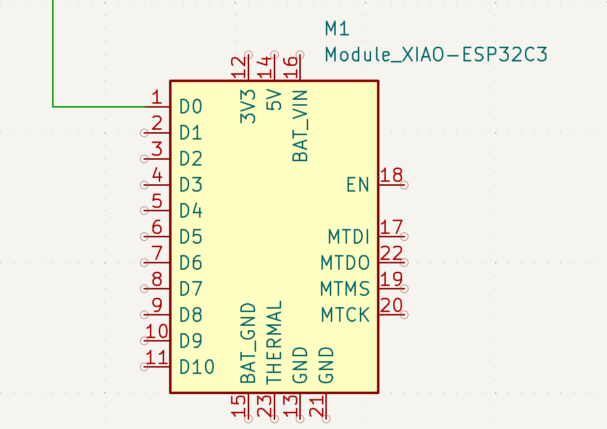
12.15 Adding the Microcontroller (XIAO ESP32C3)
The first component added to the schematic was the microcontroller. This component acts as the central processor of the system, receiving information from sensors and controlling external devices.
Using the Place Symbol tool in KiCad, I searched for the XIAO ESP32C3 module.
To make this possible, I first installed the Fab Academy electronics library, which includes ready-to-use symbols for common digital fabrication microcontrollers.
The XIAO ESP32C3 is a compact development board based on the ESP32 architecture and provides several GPIO pins that can function as analog inputs, digital outputs, and communication interfaces.
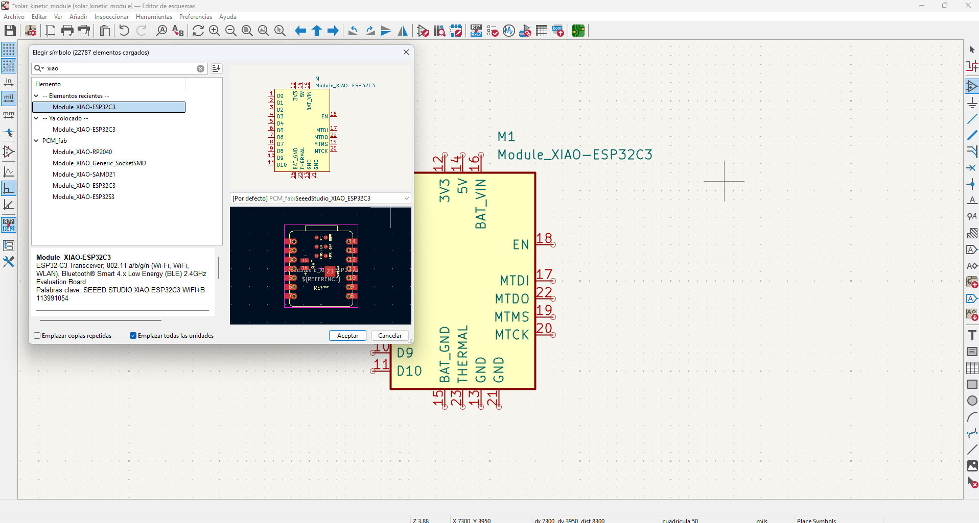
XIAO ESP32C3 microcontroller symbol added to the schematic editor.
6.16 Adding the Light Sensor (Photoresistor)
The next component added was the light sensor.
For this prototype I selected a photoresistor (LDR), a simple analog sensor whose resistance varies according to the amount of light it receives.
In KiCad this component appears as R_Photo, which represents a light-dependent resistor.
This symbol is placed in the schematic to represent the sensor that will measure environmental light levels.
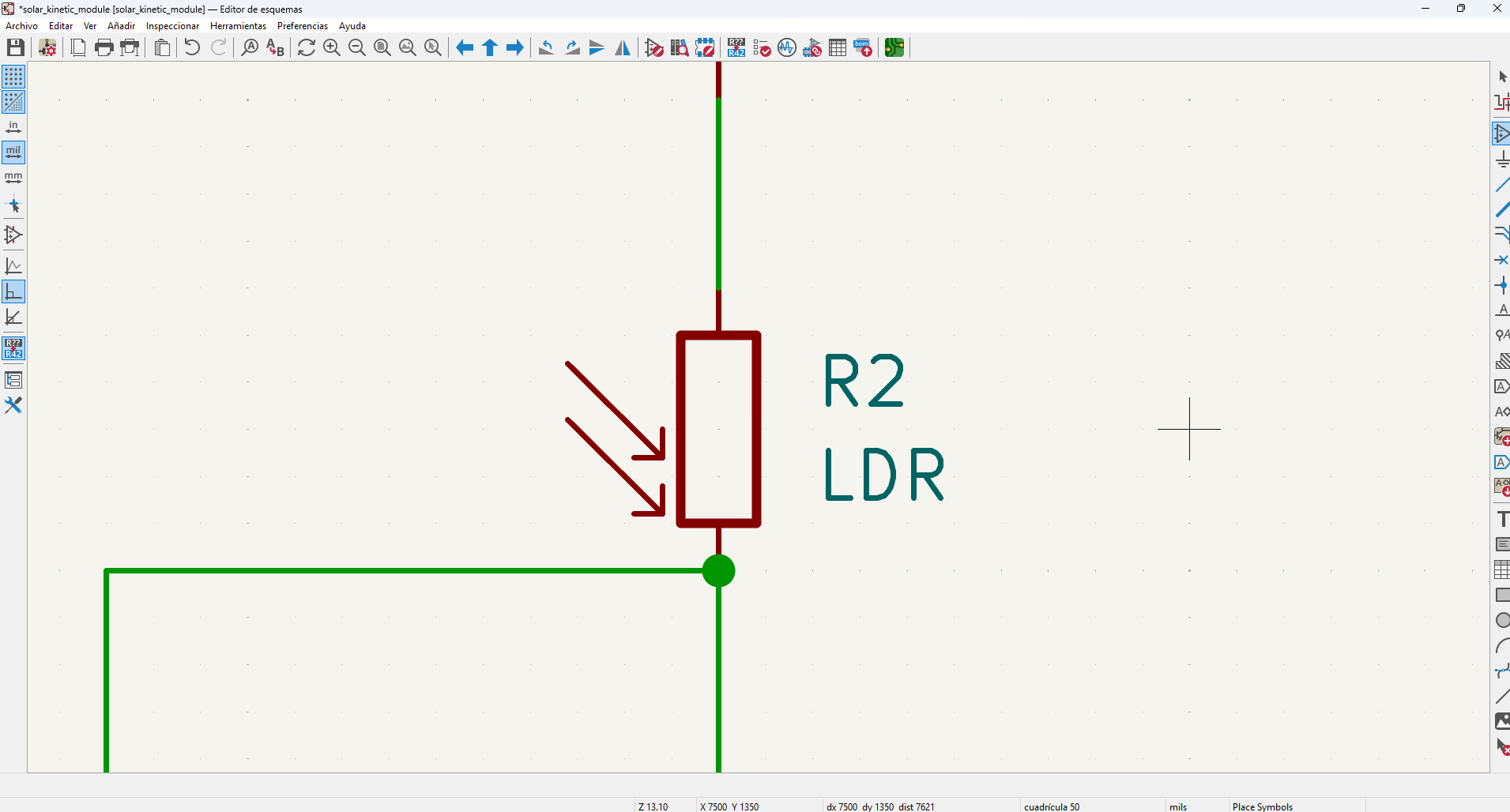
Photoresistor symbol placed in the schematic.
12.17 Adding the Fixed Resistor
To convert the sensor resistance into a readable voltage signal, the photoresistor must be combined with a fixed resistor.
This resistor forms the second half of the voltage divider circuit.
In this design I used a 10kΩ resistor, which is a common value for sensor voltage dividers.
The resistor was placed using the generic R symbol available in the KiCad libraries.
After placing the resistor, I edited its value field to define its resistance as 10kΩ.
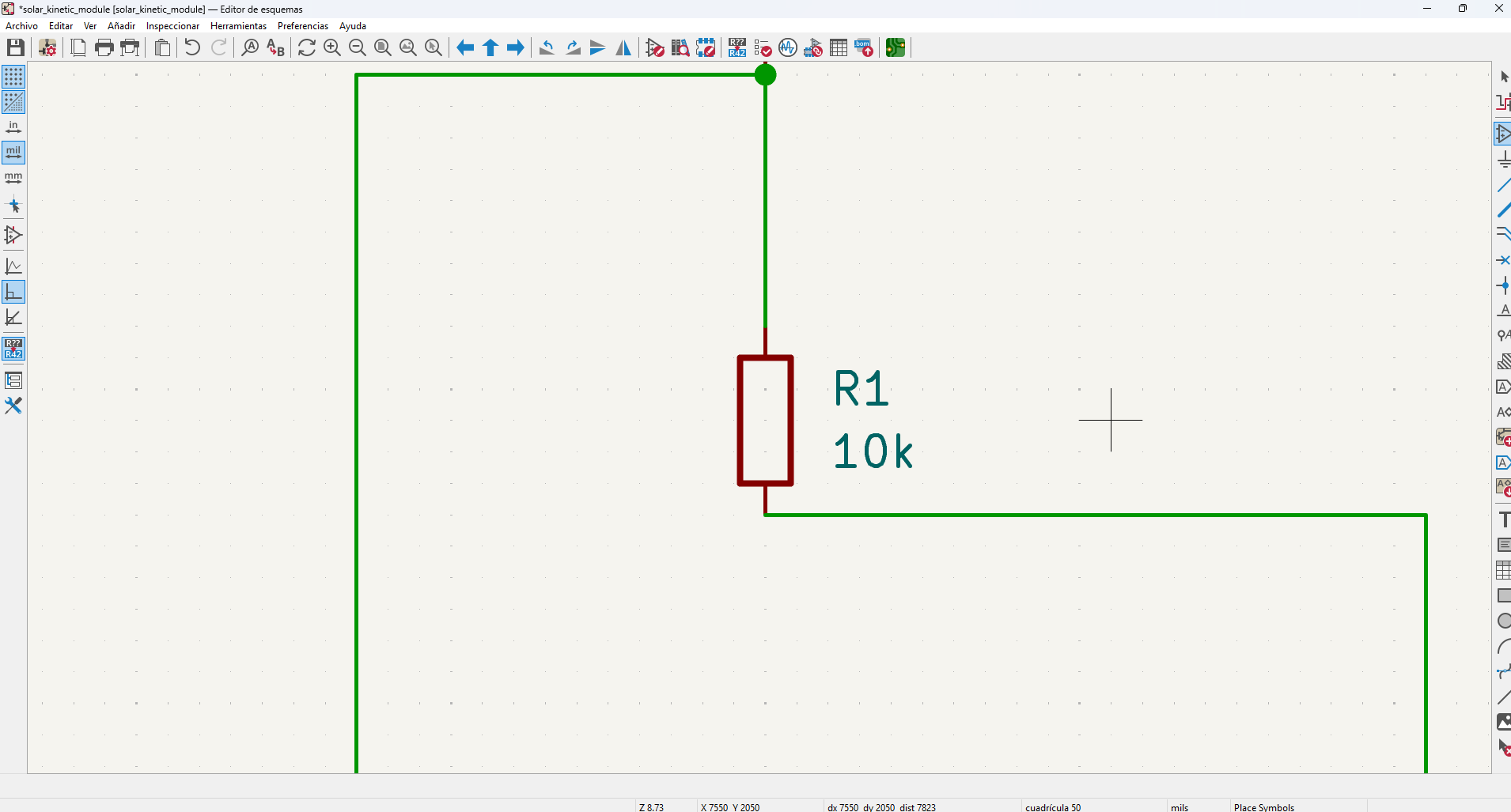
Fixed resistor added to complete the voltage divider circuit.
12.18 Connecting the Voltage Divider
After placing the sensor and resistor, the next step was connecting the components using the Draw Wires tool.
The circuit was configured as a standard voltage divider:
3.3V
 |
LDR
 |
Signal → Microcontroller analog pin
 |
10k resistor
 |
GND
The top of the photoresistor is connected to the 3.3V power line, while the bottom is connected to the resistor.
The connection point between both components acts as the analog signal node and is connected to one of the XIAO ESP32C3 analog input pins.
This allows the microcontroller to measure the voltage produced by the sensor and interpret it as light intensity.
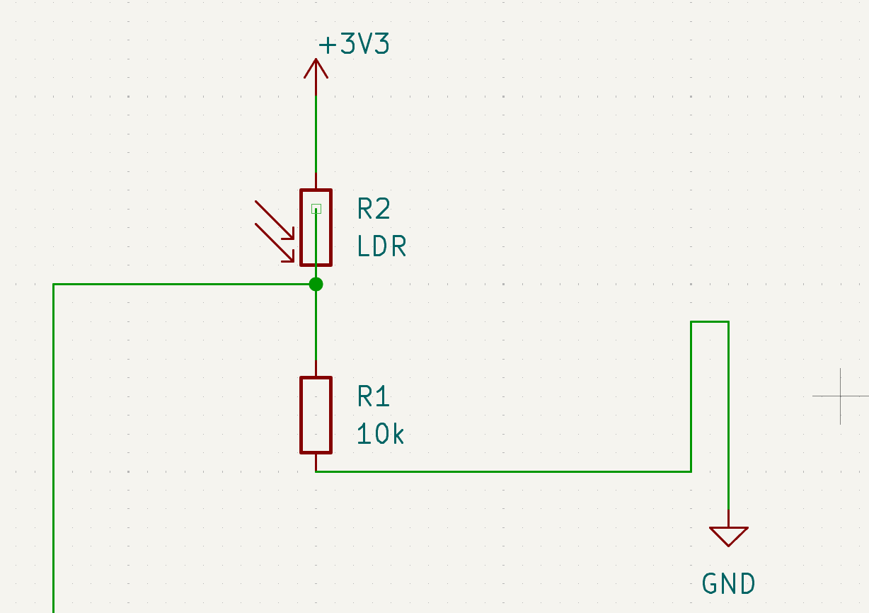
Voltage divider connections between the LDR and resistor.
6.19 Connecting the Sensor to the Microcontroller
Once the voltage divider was completed, the signal node was connected to one of the analog-capable GPIO pins of the XIAO ESP32C3.
This connection allows the microcontroller to read the voltage produced by the sensor using its internal analog-to-digital converter (ADC).
The microcontroller can then process this information and determine how the mechanical system should react.
Sensor signal connected to the XIAO ESP32C3 input pin.
12.20 Final Schematic
After completing all the connections, the schematic represents a simple environmental sensing system based on the XIAO ESP32C3 microcontroller.
This board will later act as the sensing layer of the responsive architectural module.
In the next stage of the design process, the schematic will be translated into a physical PCB layout where the components are placed and connected through copper traces.
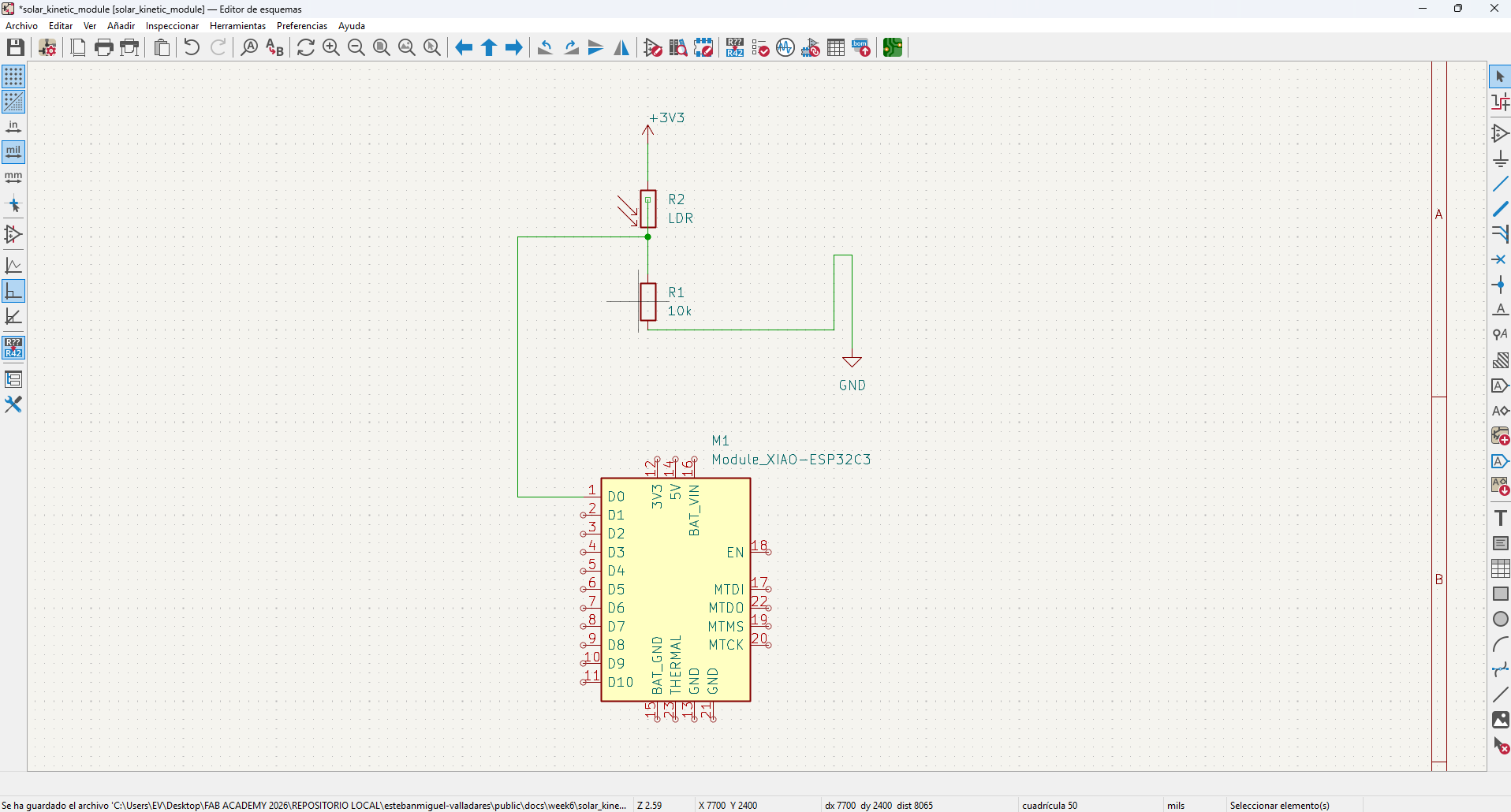
Final electronic schematic integrating the XIAO ESP32C3 with the light sensing circuit.
13.1 Current Progress
Up to this point, the electronic architecture of the system has been defined and translated into a schematic design using KiCad. The circuit integrates the XIAO ESP32C3 microcontroller with a light sensing module based on a photoresistor and a voltage divider configuration. This stage establishes the logical structure of the board and the connections required for the system to read environmental data. In the following section, I will continue the development of the project by translating this schematic into a physical PCB layout, defining component placement, routing traces, and preparing the fabrication files.