Assignment Requirements
Group assignment
- Characterize the design rules for your in-house PCB production process: document the settings for your machine.
- Document the workflow for sending a PCB to a boardhouseharacterize the laser cutter (focus, power, speed, rate, kerf, joint clearance, types).
- Document your work to the group work page and reflect on your individual page what you learned
Individual assignment
- Make and test a microcontroller development board that you designed.
Progress Status
This is for reporting progress (not for visitors to click).
Group page link + notes added.
Missing final photos and conclusions.
Upload .zip with source files.
Assignment Requirements
Learning outcomes
- Describe the process of tool-path generation, milling/laser engraving, stuffing, de-bugging and programming
- Demonstrate correct workflows and identify areas for improvement if required
Have you answered these questions?
- Linked to the group assignment page✅
- Documented how you made the toolpath✅.
- Documented how you made (milled, stuffed, soldered) the board✅.
- Documented that your board is functional✅.
- Explained any problems and how you fixed them✅.
- Uploaded your source code✅.
- Included a ‘hero shot’ of your board✅.
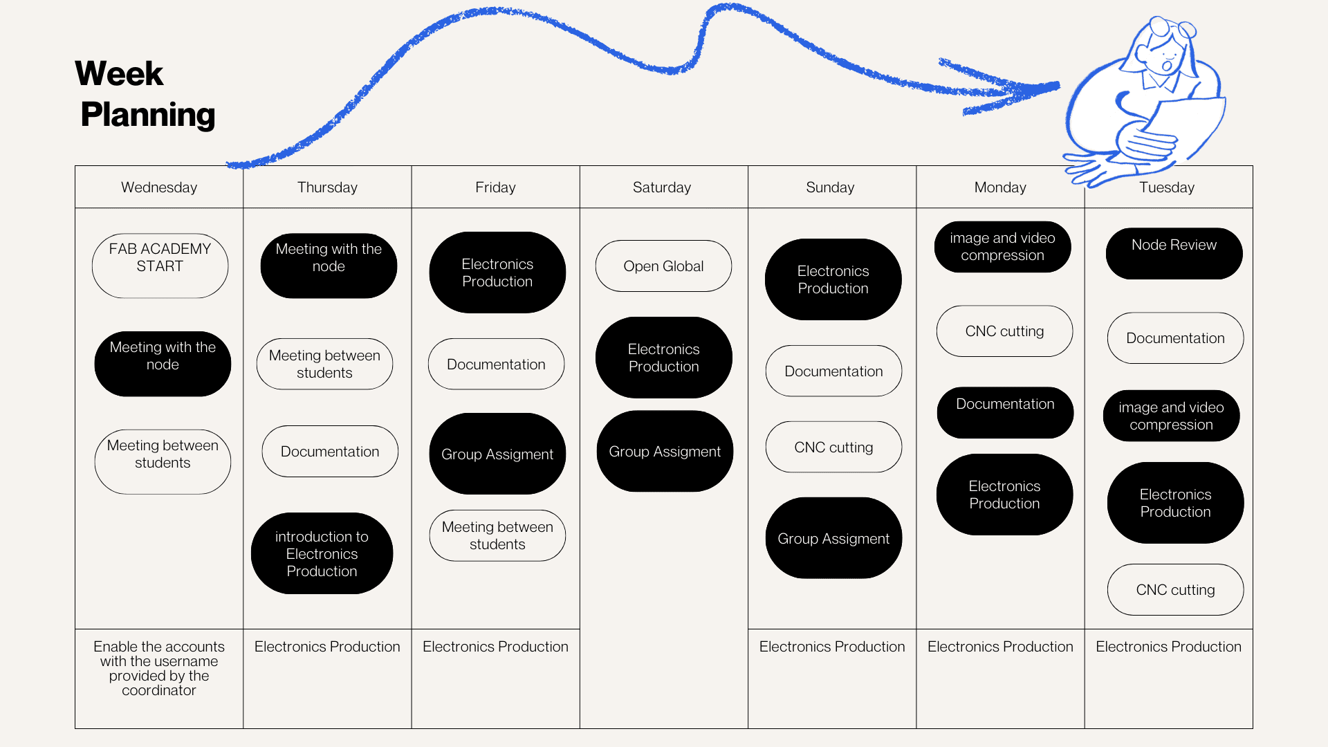
Weekly planning
During the week, we carried out various activities that presented significant challenges but were also very rewarding, especially due to the opportunity to share and learn together. We met virtually with our colleagues in the node and also participated in Open Lab meetings with Iquitos, Satipo, and Lima, which allowed us to organize and conduct open workshops in the different labs. In these sessions, we were able to review the software necessary for the work, as well as the machines, materials, and instruments required for each activity. This experience strengthened coordination between nodes and allowed us to better understand the importance of planning and managing resources effectively in digital fabrication processes.
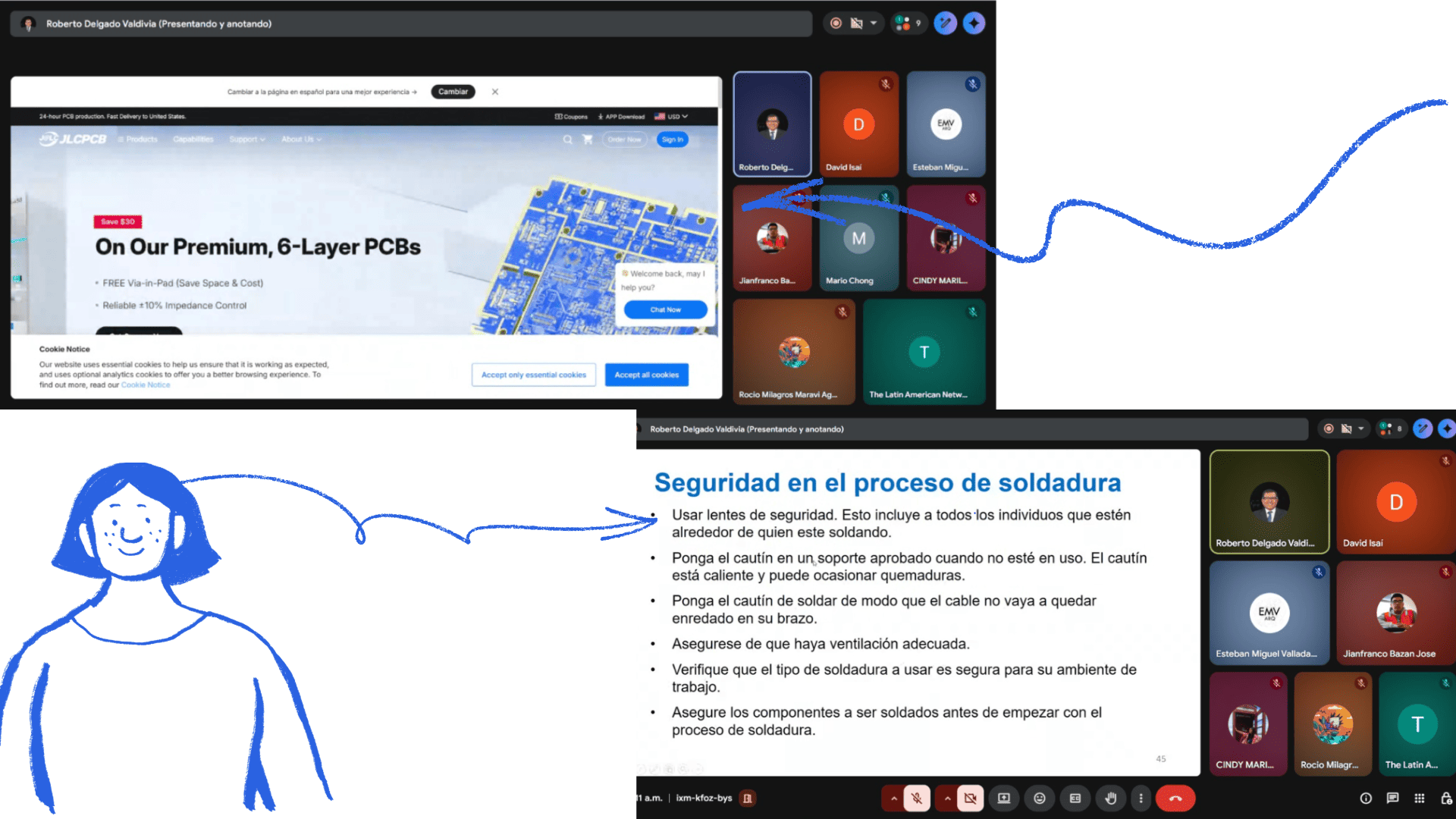
introduction Electronics Production
Professor Roberto Delgado conducted a virtual introduction to printed circuit boards (PCBs), covering materials and manufacturing methods. He also explained the soldering process, the materials and equipment used, and the necessary safety procedures for these activities.
This information was fundamental to the group project, as it allowed us to understand the characteristics of the machines and receive practical recommendations based on his experience. We also learned about the manufacturing process using MODS and how to identify common problems, such as poor or incorrect soldering.
Finally, the importance of safety during the soldering process was reinforced, highlighting best practices to avoid risks and improve the quality of the work.
For more information, visit the following page: Learn more about PCB manufacturing
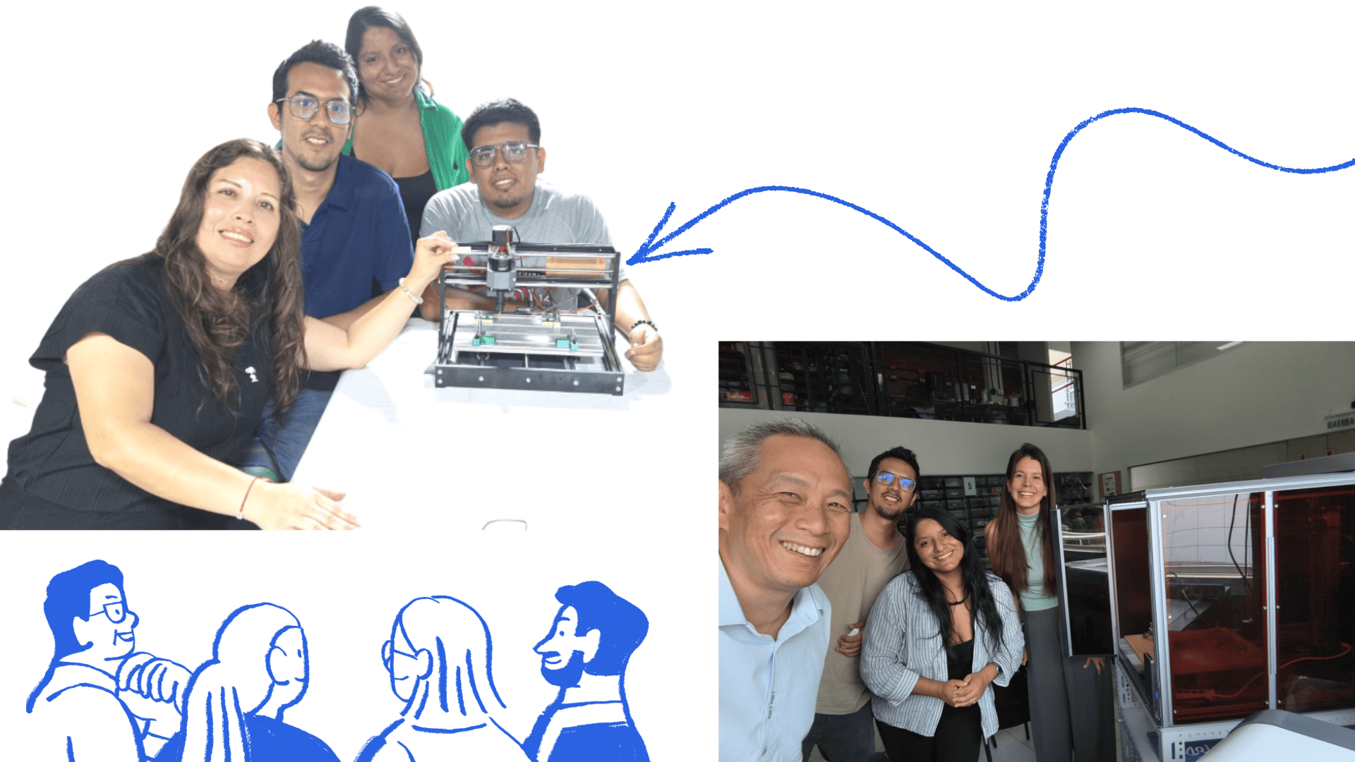
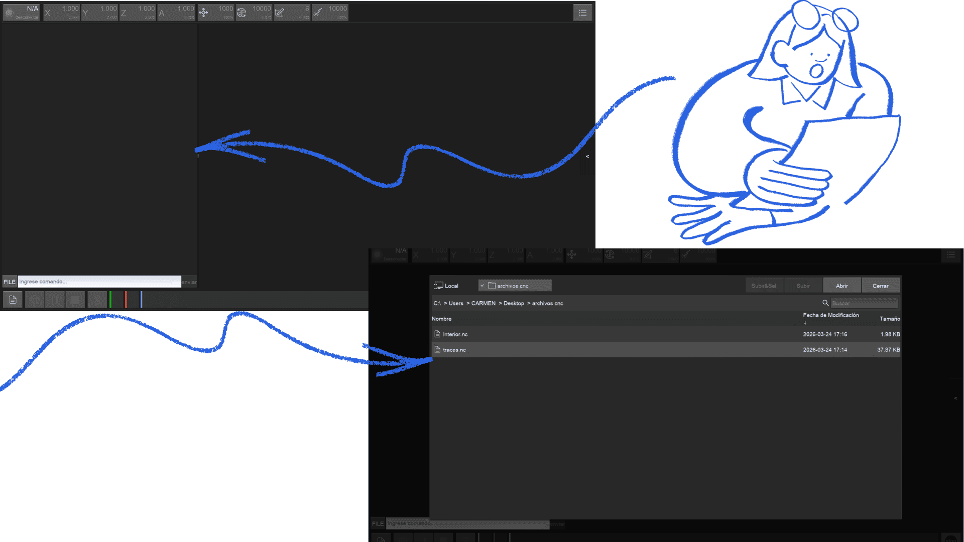
Group Work
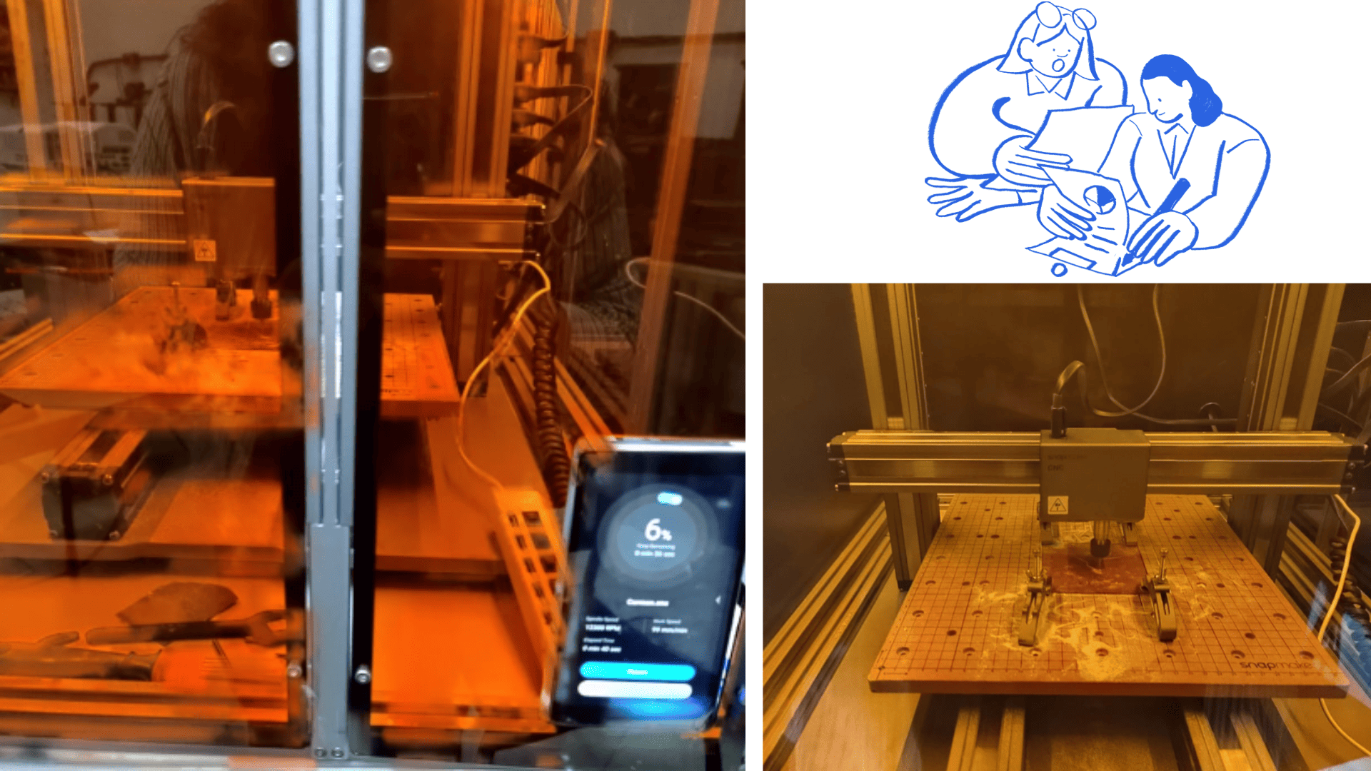
Teamwork allowed us to meet in different locations and use the CNC tool at one of Fab Lab Lima's mobile labs. We also met with Silvana Espinozza , who provided support in using the mobile Fab Lab's CNC machine, helping us resolve some questions that arose during the process.
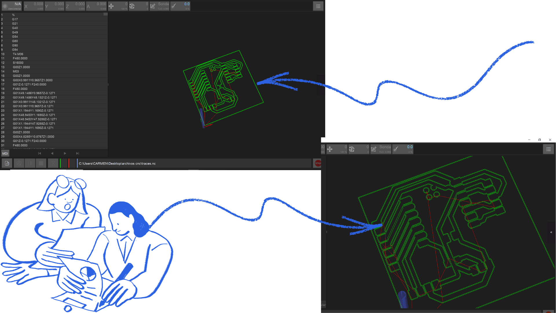
As a team, we actively collaborated to understand the PCB production process. We explored how to properly prepare design files, generate toolpaths, and configure the CNC milling machine for both trace milling and board cutting.
During the process, we tested different parameters, such as depth of cut, feed rate, and tool selection, with the goal of achieving clean and precise milling of the printed circuit board. These tests allowed us to identify the appropriate settings and avoid common problems, such as incomplete traces or board damage.
Through this collaborative work, we gained a better understanding of the entire PCB manufacturing flow, recognizing how small adjustments to parameters can significantly influence the final result.
This experience was fundamental in strengthening our knowledge and ensuring the success of our individual PCB designs.
For more details about the group assignment, visit the group page .
Personal Reflection
Through the group work, I developed a deeper understanding of the printed circuit board (PCB) manufacturing process, from file preparation to final machining using the CNC machine. Being part of the team allowed me to observe how different parameters affect the results and how careful adjustments can improve precision and reduce errors.
I also strengthened my skills in using digital tools such as FlatCAM and gained more confidence in operating manufacturing equipment. This experience helped me understand the importance of proper setup, planning, and attention to detail before starting the machining process.
Additionally, working collaboratively helped me learn from others, solve problems more efficiently, and adapt to different approaches. Overall, this experience improved my technical knowledge and gave me more confidence to design and manufacture my own PCBs independently.
Individual Assignment
| Artículo | Componentes | Cantidad |
|---|---|---|
| Microcontrolador | ESP32-C3 (XIAO ESP32-C3) | 1 |
| Sensor de temperatura y humedad | DHT11 | 1 |
| Sensor de luz | LDR | 1 |
| Actuador | Servomotor | 1 |
| Pantalla | OLED (I2C) | 1 |
| Interruptor | Switch SPDT | 1 |
| LED indicador | LED | 1 |
| Resistencia | Resistor | 1 |
| Conector de batería | Entrada 5V | 1 |
| Pines externos | Header de pines | 1 |
General Features
3-in-1 Technology: 3D Printing + Laser Cutting + CNC
Frame: All-metal construction (aluminum)
Design: Modular (interchangeable tools)
Display: 5-inch touchscreen
Connectivity: WiFi, USB, USB flash drive
Software: Snapmaker Luban
CNC Features (Snapmaker A350T)
Work area: 320 × 350 × 275 mm
Spindle speed: 6,000 – 12,000 RPM
Compatible tool diameter: 0.5 mm – 6.35 mm (ER11 collet)
Clamping system: MDF base with clamps
Machining type: CNC milling and engraving
Compatible Materials
Wood
Acrylic
PCB (electronic boards)
Carbon fiber
POM and other plastics
Functions
Contour cutting
Surface engraving
PCB manufacturing
Carving of soft materials
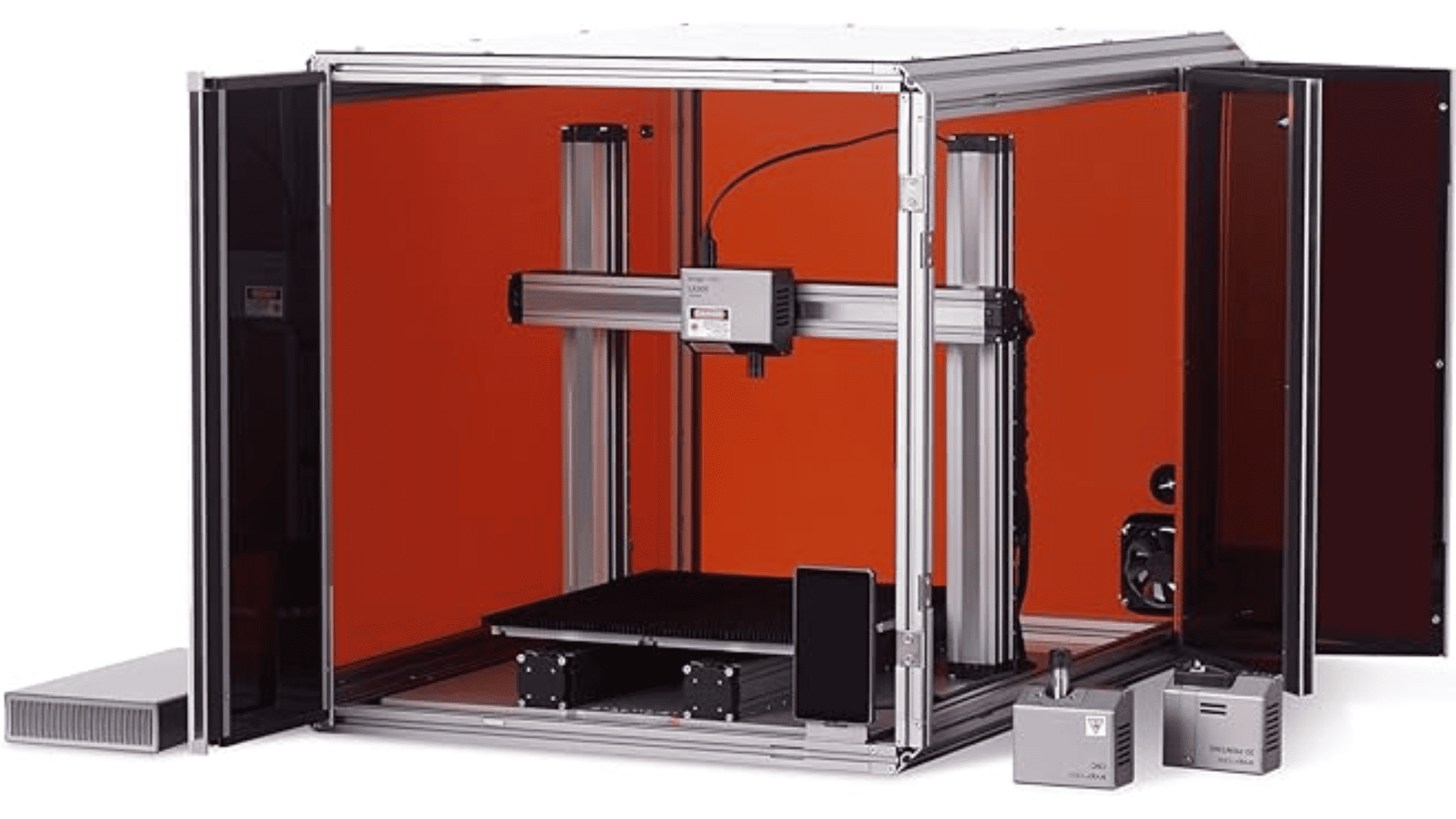
SNAPMAKER
Testing on the milling machine
The steps followed in this process were as follows: first, the PCB design was created using KiCad. Once the design was completed, the Gerber files were exported, which contain the necessary information for manufacturing the board.
Next, the Gerber files were imported into FlatCAM, where the machining parameters were configured, such as tool diameter, cutting depth, and feed rate. After this configuration, the G-code was generated both for engraving the PCB traces and for cutting the board outline.
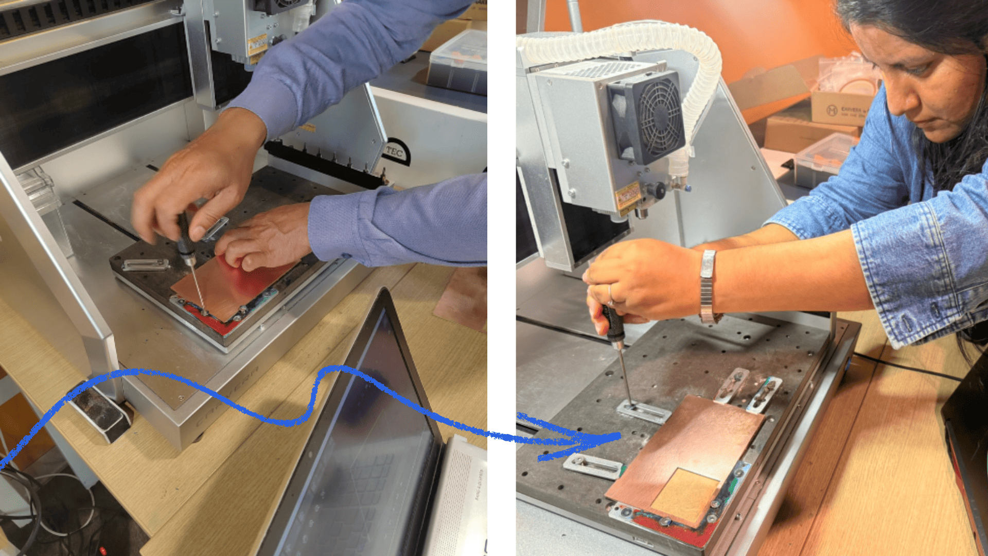
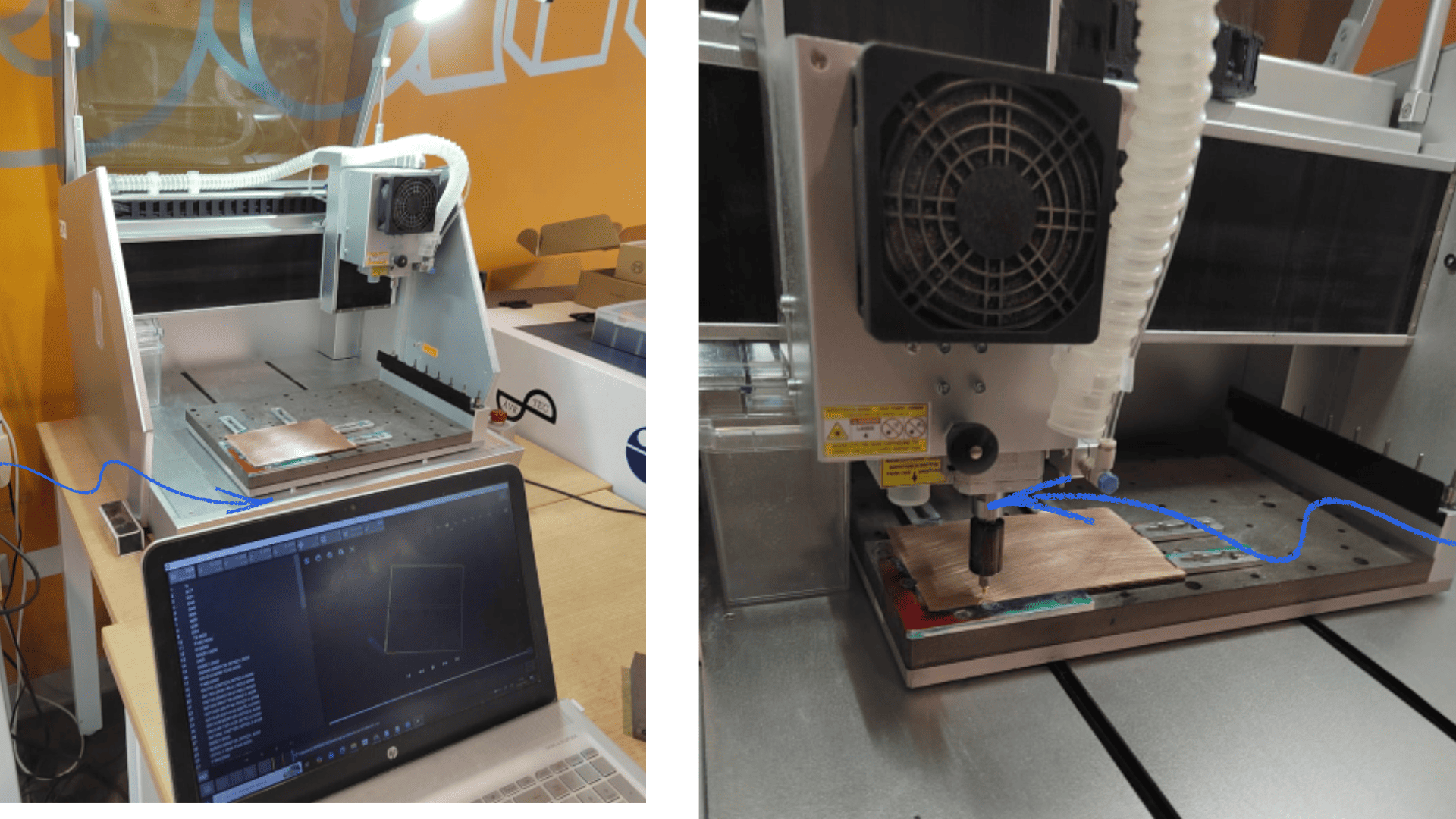
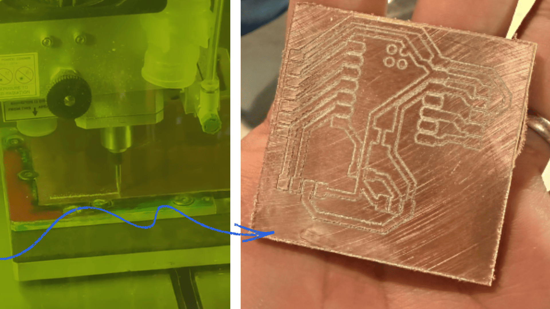
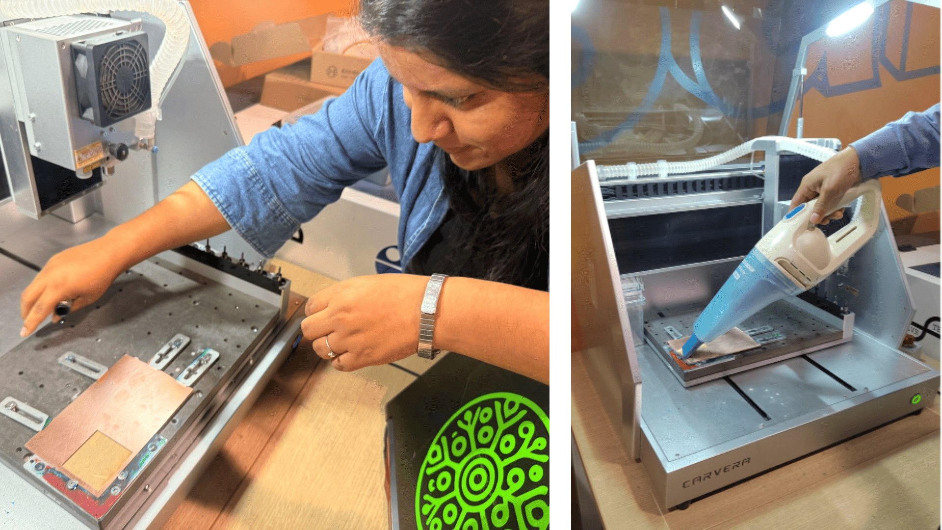
The generated G-code was then transferred to the CNC machine. Before starting the machining process, the copper-clad board (baquelite) was carefully placed and securely fixed on the machine bed to ensure stability and precision.
Once everything was properly set up, the CNC machine was operated to mill the traces according to the design. The machine followed the G-code instructions to accurately carve the circuit paths on the board.
Finally, the soldering process was carried out. Although it can be complex, with careful handling, proper tools, and attention to detail, it is possible to achieve good results and ensure correct electrical connections between the components.
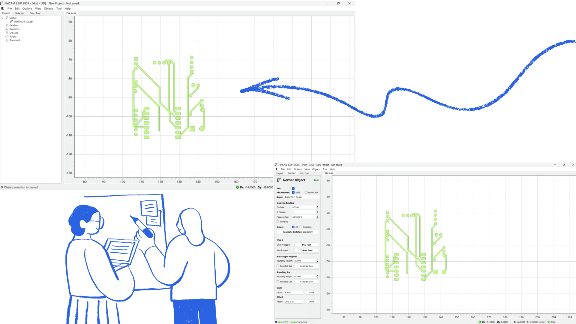
The Gerber files of the PCB design were imported into the FlatCAM software to prepare for the electronic board manufacturing process.
Next, the necessary machining parameters were set, including the tool diameter, depth of cut, and feed rate, ensuring accuracy during milling.
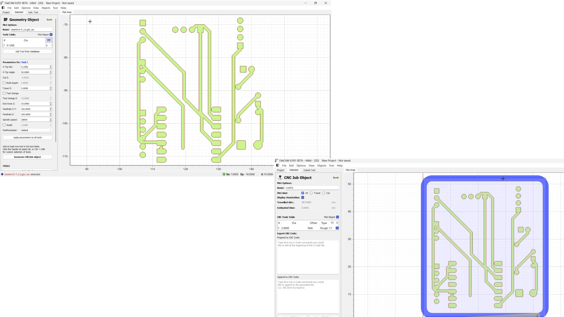
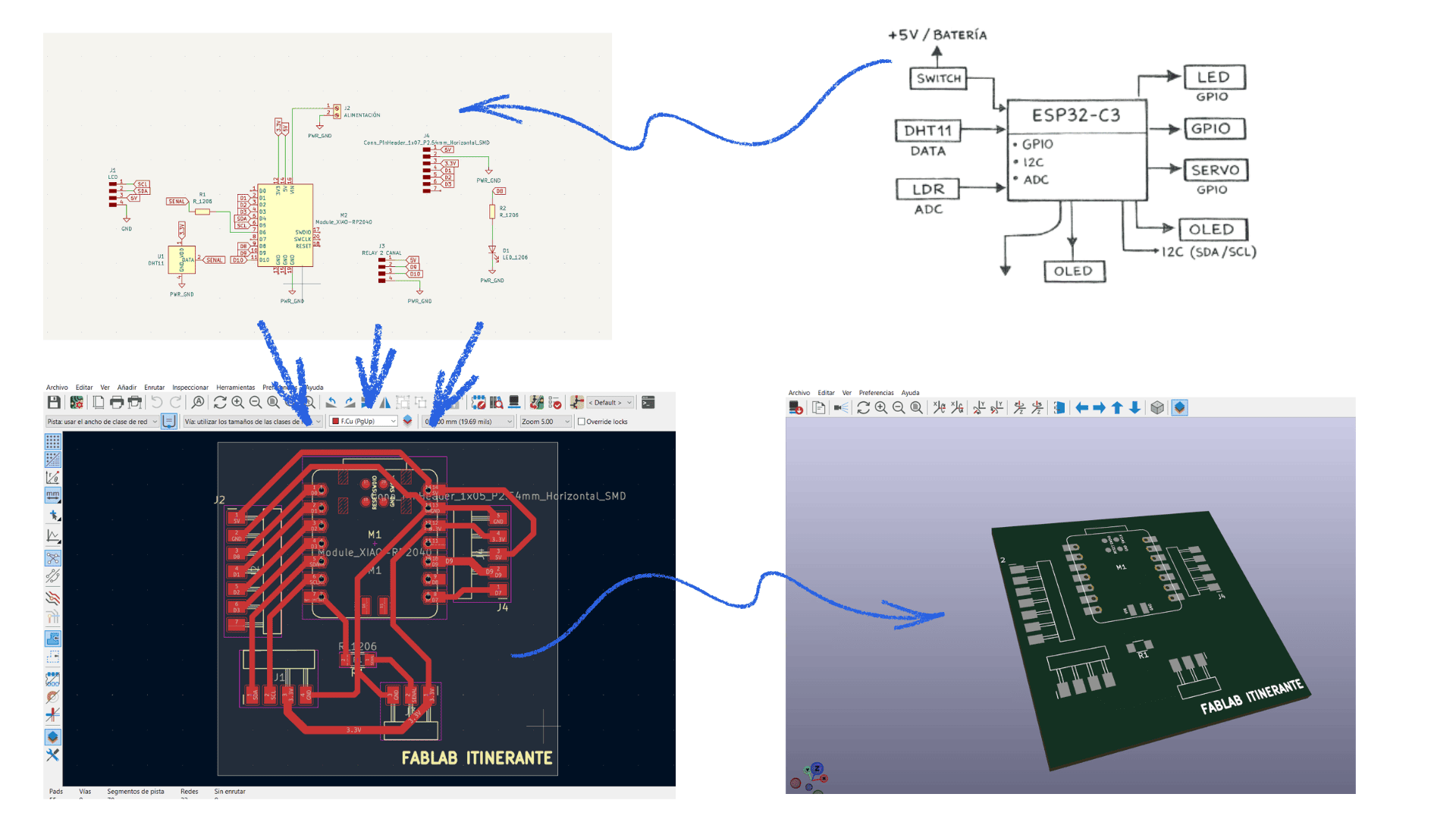
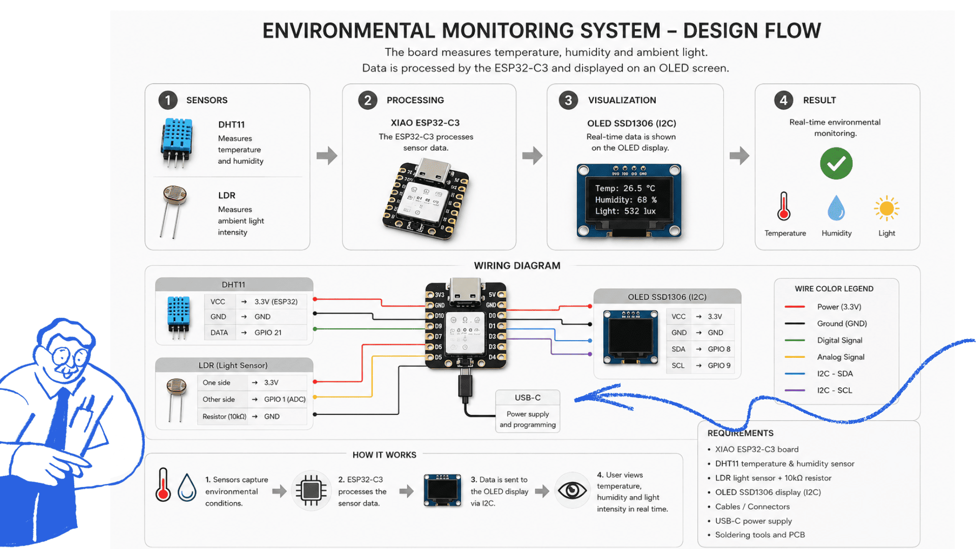
The diagram illustrates the basic operation of the system with the ESP32-C3 as the main controller. The DHT11 sensor measures temperature and humidity, the LDR sensor detects ambient light, and the OLED display shows the information via I2C communication. Additionally, the system controls an LED and a servo motor using GPIO pins, all powered by a 5V battery with a power switch.
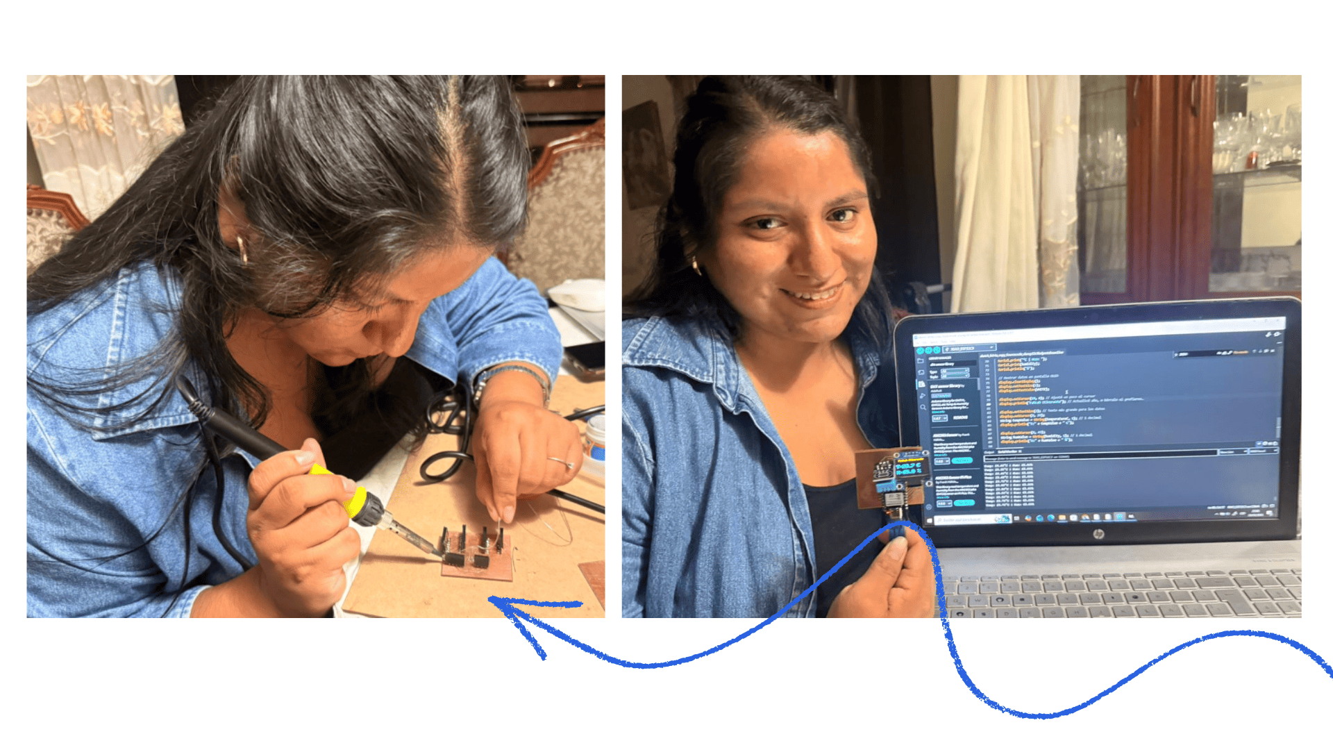
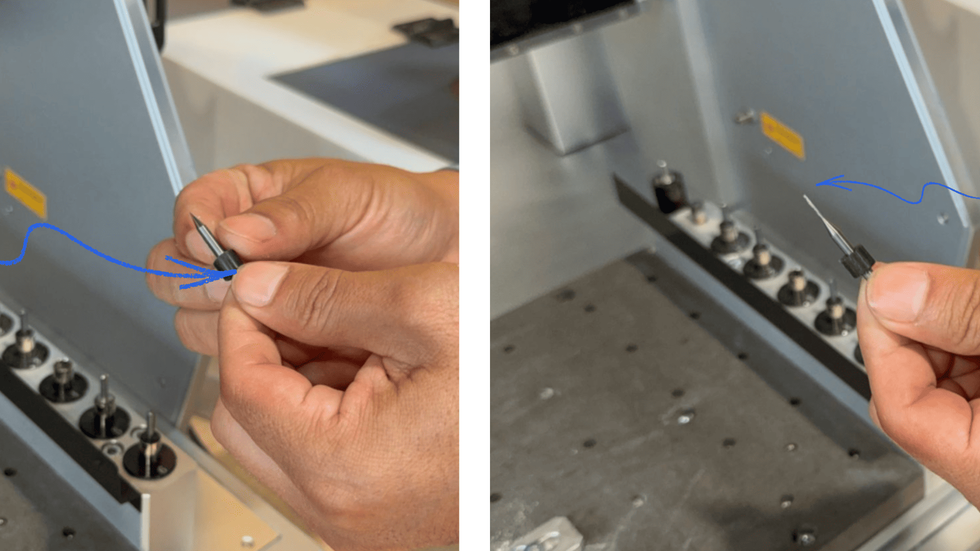
You can see the work table equipped with the soldering station, the precision magnifying glass and the solder, essential tools for assembling and soldering electronic components with greater precision and safety.
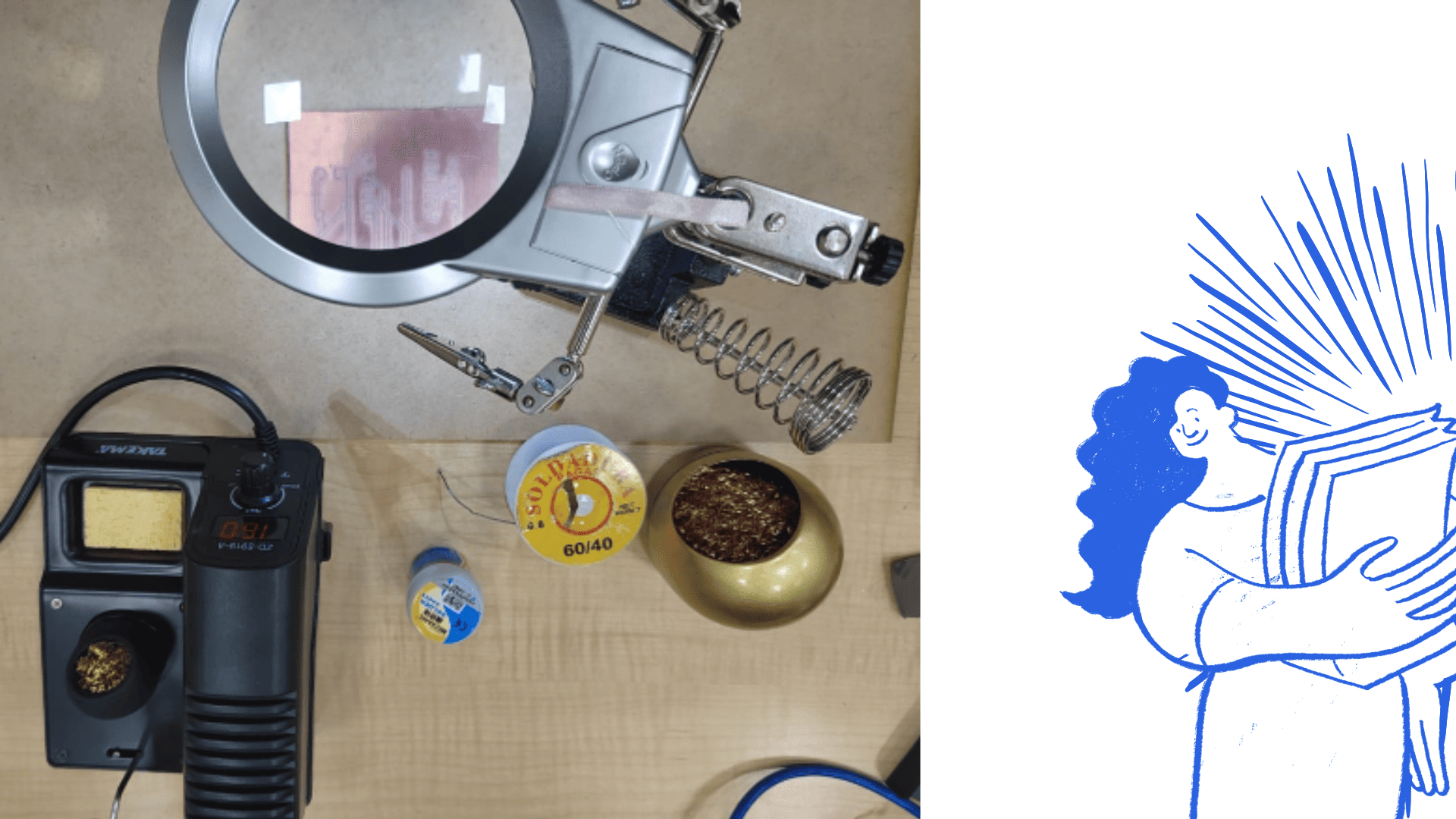
cDry chemical fire extinguisher available near the work area.
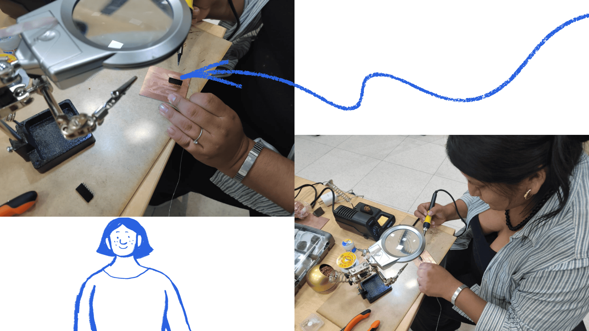
The soldering process of the electronic board, previously manufactured on the CNC machine, can be observed, using the soldering station, solder, and precision tools to correctly assemble the electronic components.
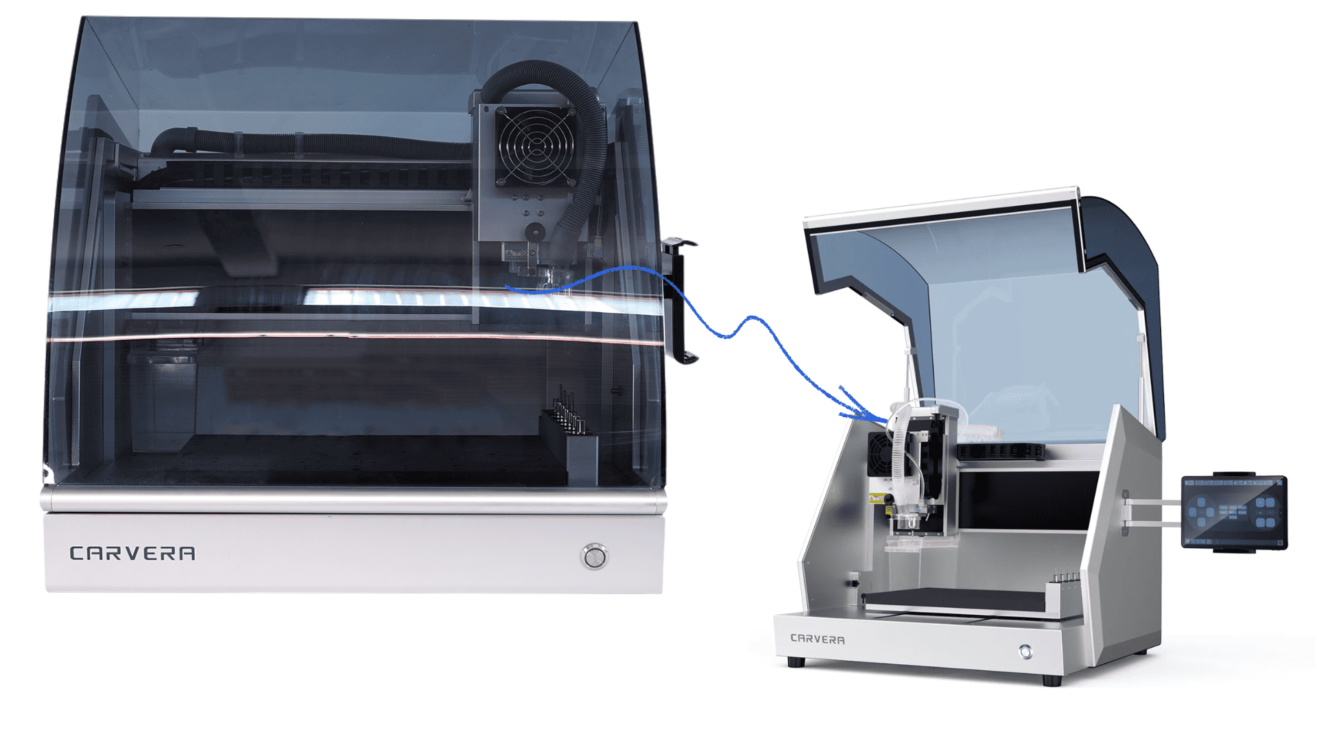
Carvera CNC Machine
The CARVERA Maker is an advanced and intelligent desktop CNC machine designed to meet the demands of digital manufacturing in confined spaces. Despite its compact size, it offers a high level of precision, automation, and versatility, making it an ideal tool for designers, engineers, and machining enthusiasts.
It integrates innovative features such as automatic leveling, automatic tool change, a dust collection system, and the option to add a 4-axis module. Thanks to these features, CARVERA sets a new standard in desktop CNC machining.
One of its main advantages is the automatic tool change system along with the automatic probe function. With machines lacking these functionalities, the user must manually perform tool changes and calibration, which is tedious and time-consuming, especially for complex tasks like PCB manufacturing.
In contrast, CARVERA allows for the automated execution of multiple processes—such as leveling, cutting, cleaning, drilling, and engraving—selecting the appropriate tool at each stage. This not only optimizes working time, but also improves the accuracy and quality of the final result, allowing the user to focus primarily on the design.
Motherboard
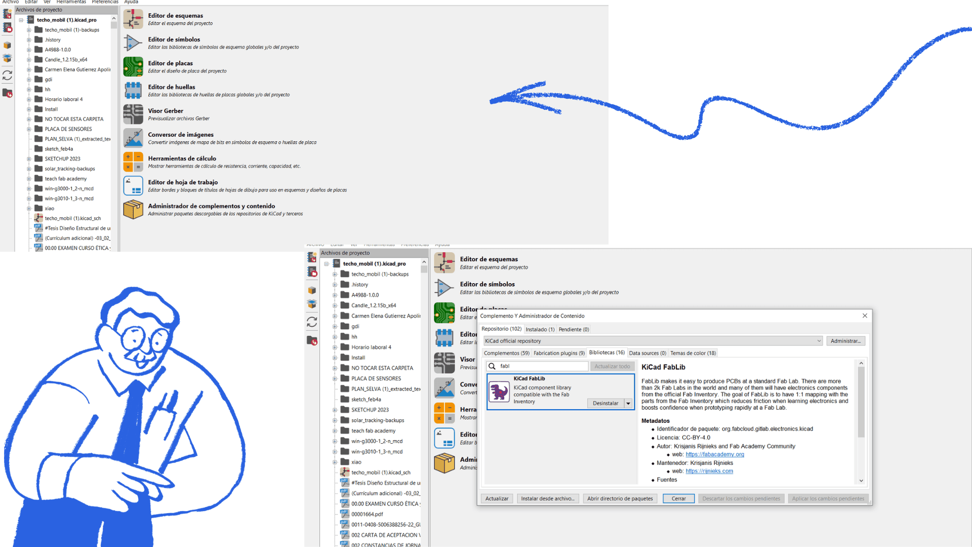
Work began using the KiCad program, after verifying that all necessary libraries were correctly installed. The motherboard file was also opened for review, ensuring the FabLab library was properly incorporated.
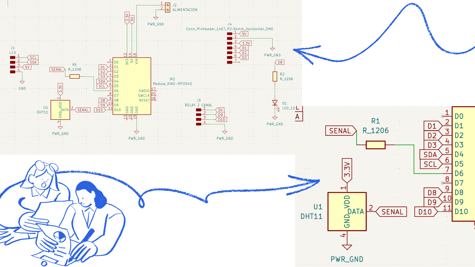
From this motherboard, the required components were selected and adapted. First, the XIAO microcontroller was chosen, specifically the Xiao ESP32-C3 model. The footprints for each component were also verified, guaranteeing their compatibility with the design. Subsequently, the electronic schematic was updated.
During the schematic design, the various components, such as the DHT sensor and the OLED display, were placed and properly connected to the ESP32-C3. The microcontroller's technical specifications were consulted to ensure correct pin assignment and proper circuit operation.
Using a motherboard optimized the design process; however, it also required additional adjustments and validations to correctly integrate the new components into the existing circuit.
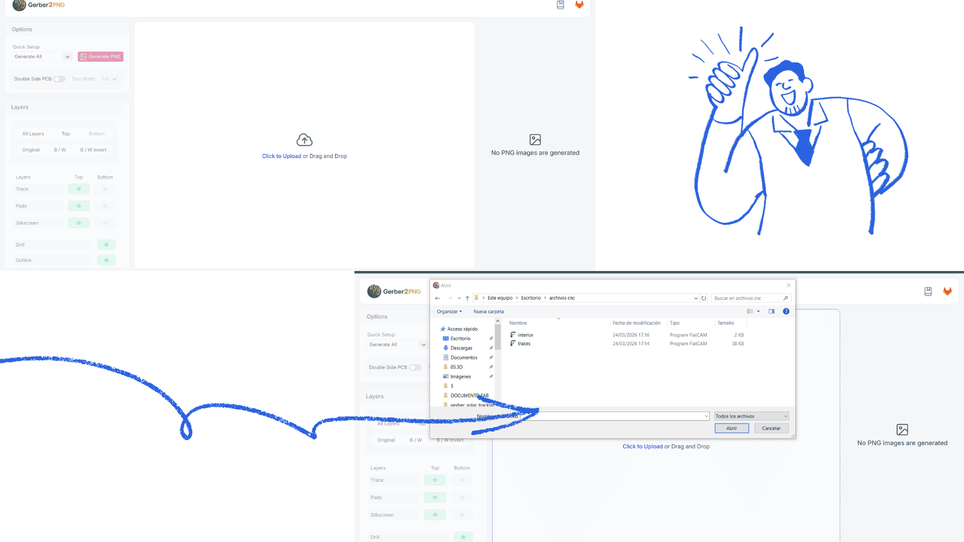
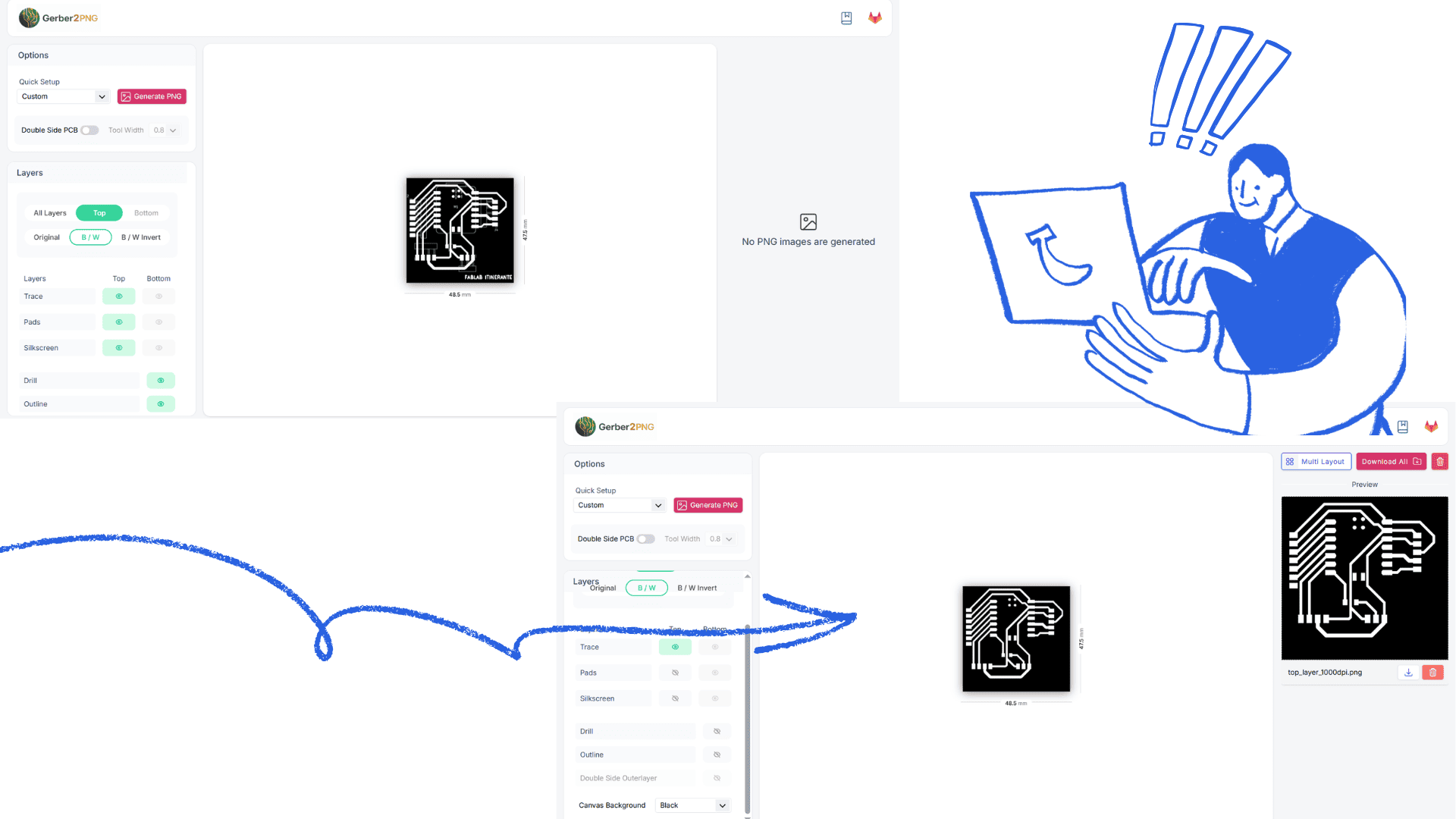
Gerber to PNG Conversion
Gerber2PNG is the process (or tool) that allows you to convert Gerber files into PNG images. This is very useful when you need to use PCB designs on CNC milling machines, such as in a Fab Lab.
What is it used for?
- Converting the PCB design into an image that can be interpreted by machining software (such as mods)
- Generating toolpaths
- Quickly visualizing the design layers
Workflow
- Design the PCB in KiCad
- Export the Gerber files
- Use Gerber2PNG to convert to an image
- Import the PNG into mods or other software
- Machine the design on the CNC (e.g., Carvera)
Mods configuration
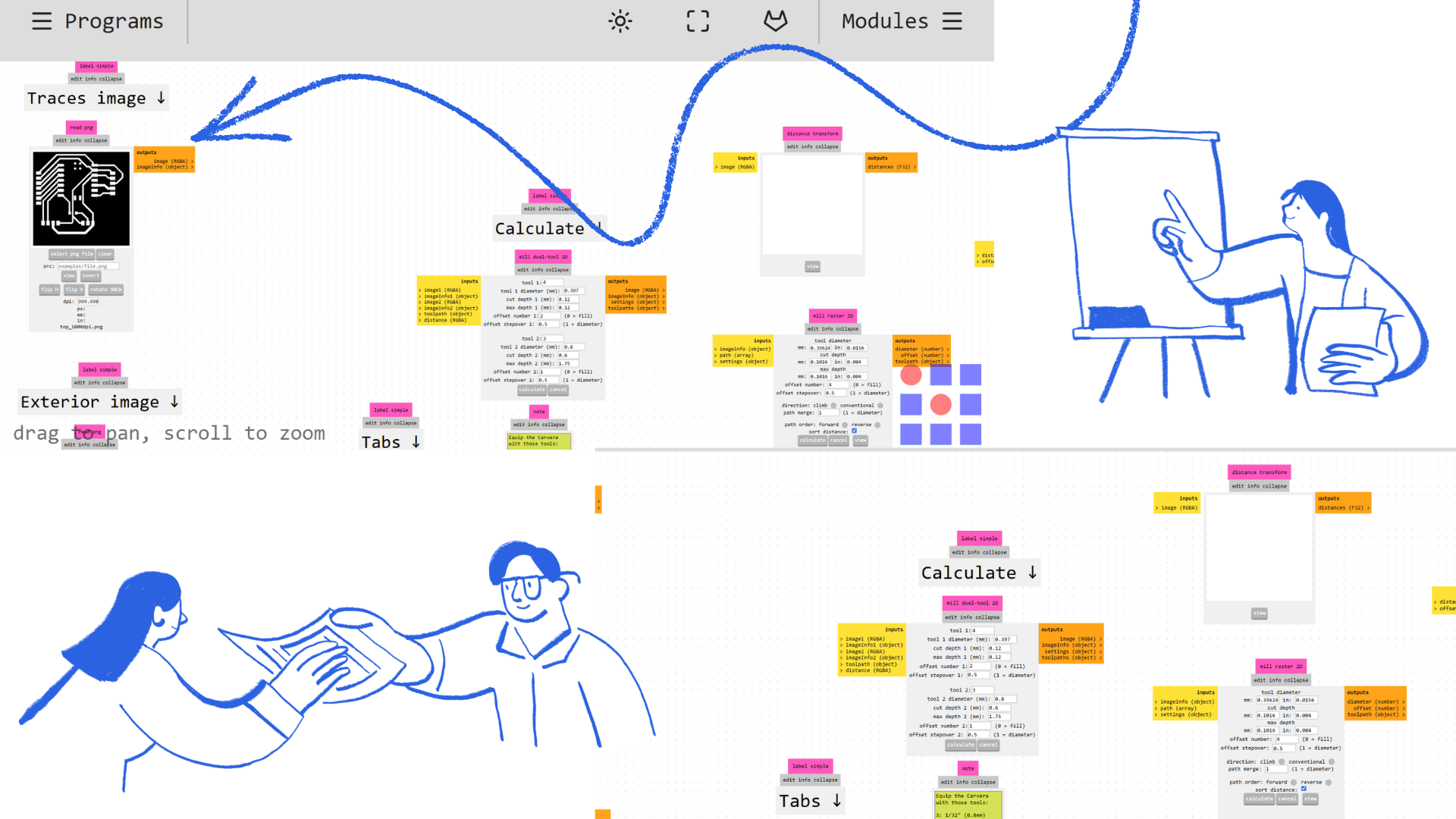
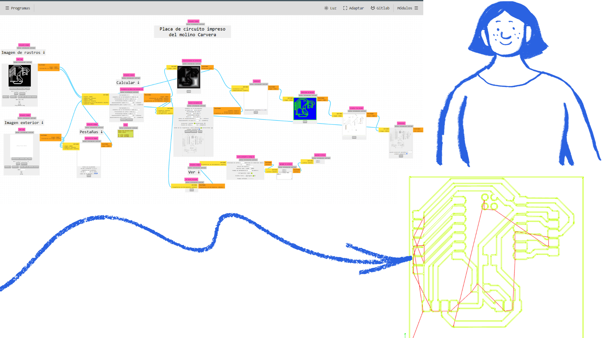
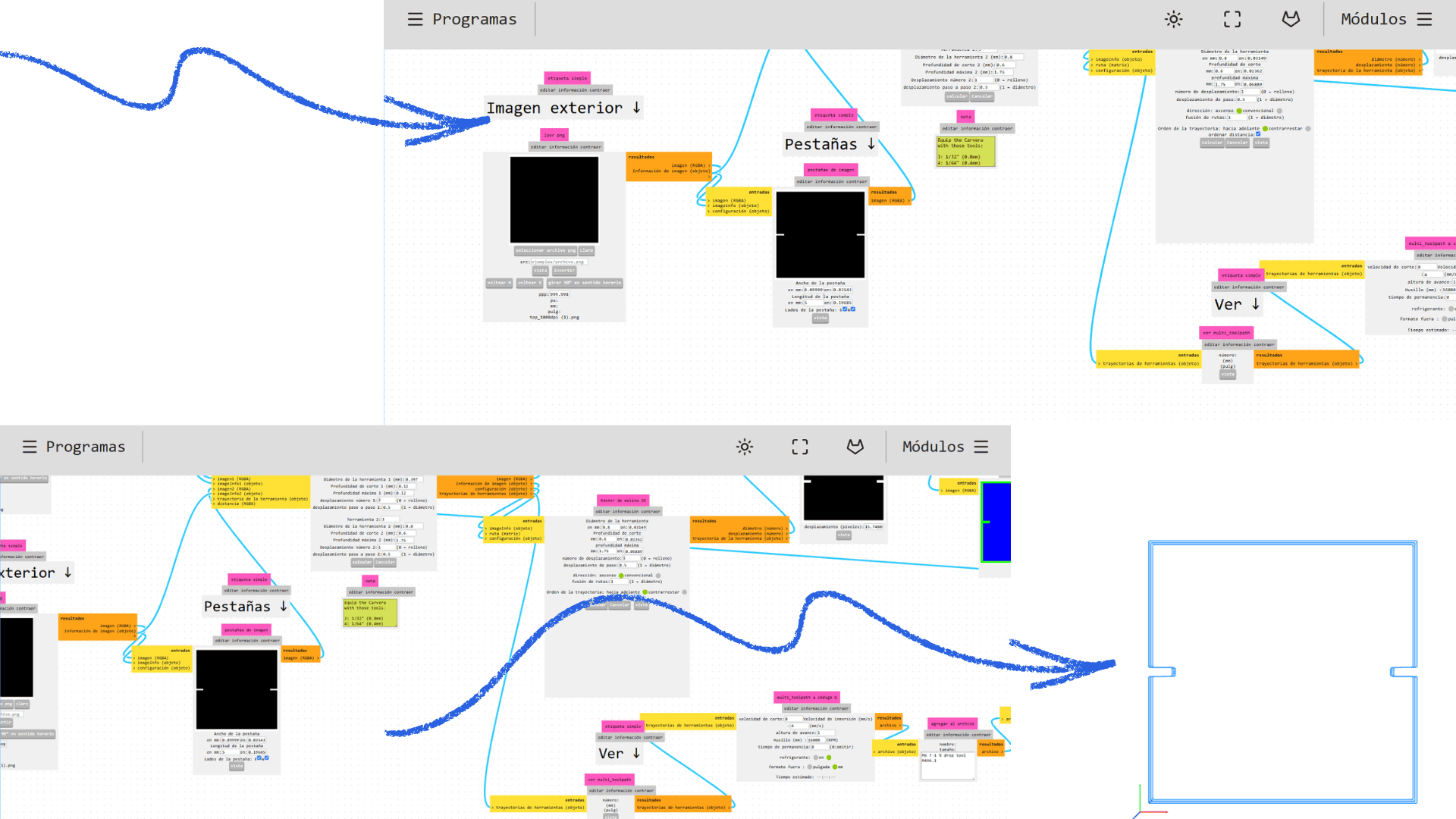
After designing the board in KiCad, the Gerber file was exported and processed in Gerber2PNG to obtain the SVG file. This file was imported into Mods, where the color inversion function was used to generate an inverted version of the design. This step facilitated the visualization of the board, allowing for clearer identification of the components and connection paths.
Next, the parameters in the Mill Raster 2D settings were adjusted, and the corresponding calculations were performed to obtain the updated machining paths. Modifying these values allowed for refining the milling parameters, resulting in a more precise and efficient process.
These adjustments were applied to both the internal machining (tracks) and the external cutting of the board. This optimized the milling strategy according to the specific needs of the project, significantly improving the quality and accuracy of the final result.
Carvera Controller
0First, open a web browser and go to the official Makera website. Then, locate the "Support" or "Downloads" section in the main menu. Within this section, search for the software called Carvera Controller.
Next, select the program version according to your computer's operating system (Windows or macOS) and click download. Once the file has downloaded, open the installer and follow the instructions to complete the installation.
Finally, run the Carvera Controller program to begin configuring and using your Carvera CNC machine.
PCB Fabrication Analysis
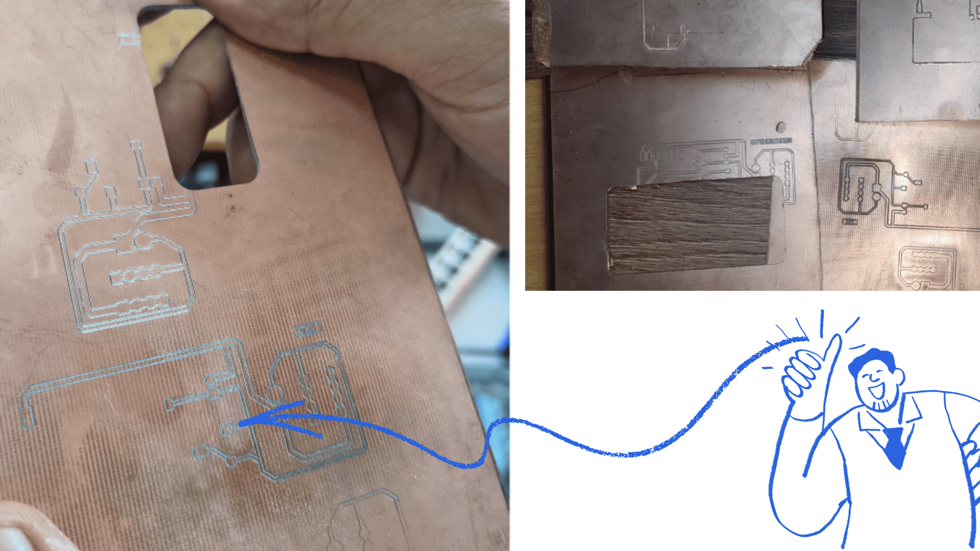
The PCB fabrication process presented some technical challenges mainly related to copper cleaning, shallow engraving, and irregular milling depth. Although the PCB traces were correctly designed and most electrical connections worked properly, some areas of the board showed inconsistent cutting depth during the milling process.
To improve the final PCB finish and ensure proper functionality, the following technical procedure was performed:
- The copper surface was initially inspected before milling to ensure correct positioning and proper fixation of the PCB material on the machine bed.
- During the milling process, some areas showed shallow engraving caused by slight surface leveling variations and Z-axis calibration inconsistencies.
- After the machining process was completed, a handheld vacuum cleaner was used to remove copper dust, debris, and particles generated during milling.
-
The PCB surface was then manually polished using fine sandpaper in order to:
- remove residual copper particles,
- improve trace visibility,
- reduce surface imperfections,
- and obtain a cleaner and more uniform finish.
- A visual inspection was performed to verify trace continuity, proper separation between traces, and possible remaining copper residues.
- The Z-axis calibration and machine bed leveling were also reviewed to improve cutting depth consistency in future PCB fabrication iterations.
- Finally, electrical and functional tests were performed to validate the correct operation of the PCB and the communication between the XIAO ESP32-C3, DHT11 sensor, and OLED display.
Despite the irregularities observed during fabrication, the PCB operated successfully and allowed proper validation of the electronic system. This process helped improve the understanding of machine calibration, copper surface preparation, cleaning procedures, and milling depth control during digital PCB fabrication.
PCB Cutting and Soldering
After verifying that all necessary libraries were correctly installed, the PCB design process began in KiCad using a motherboard with the XIAO ESP32-C3 microcontroller. Components such as the DHT sensor and OLED display were incorporated, validating the connections and correct pin assignments.
Subsequently, the PCB design was exported as Gerber files and converted to PNG format using Gerber2PNG, allowing the generation of machining paths for the Carvera CNC machine.
Finally, the PCB was cut and etched on the CNC machine, followed by the soldering of the electronic components using a soldering station, solder, and precision tools to complete the circuit assembly.
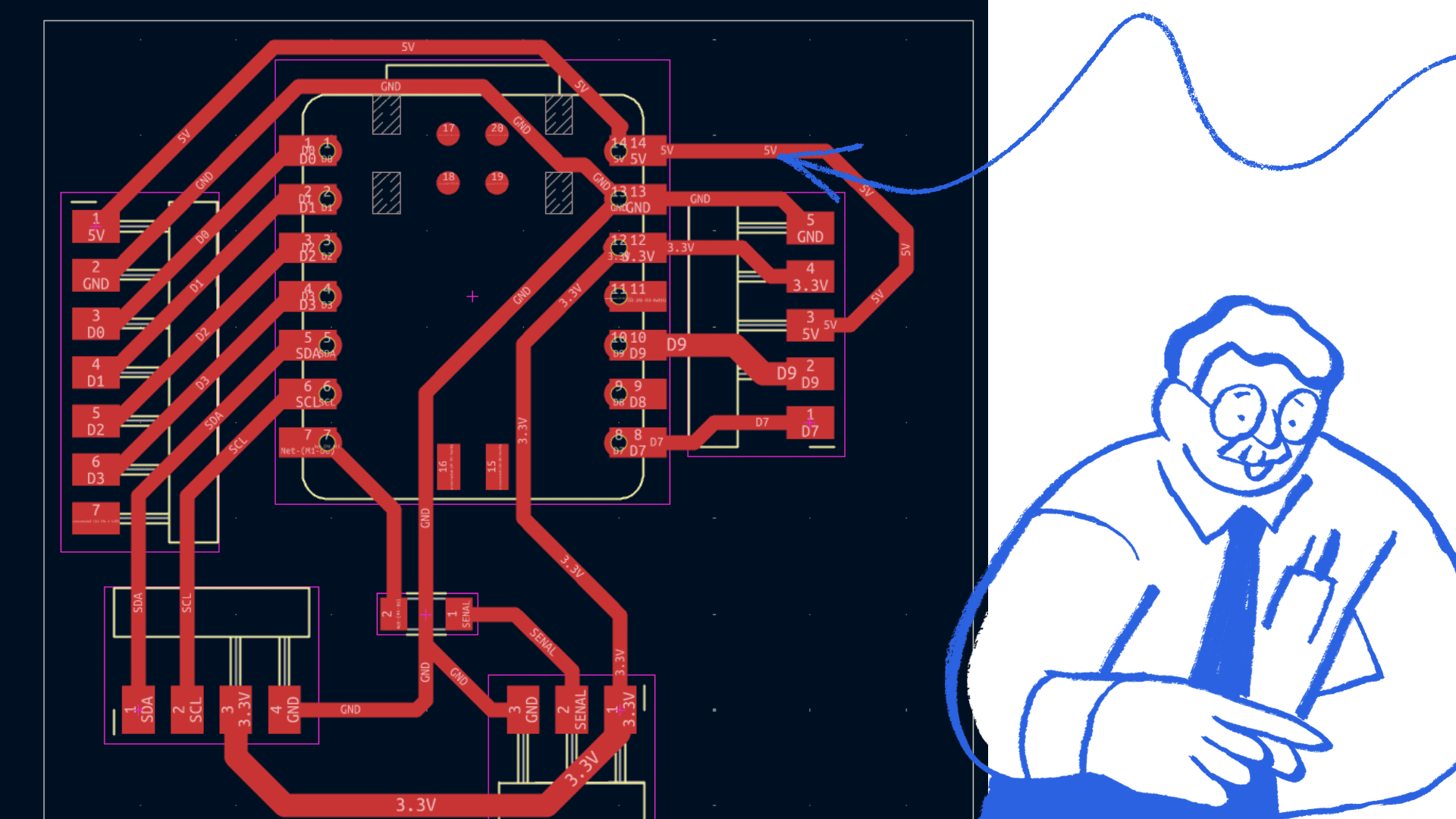
El diagrama PCB fue diseñado en el software KiCad, donde se organizaron y conectaron los componentes electrónicos del circuito. A través del esquema y el diseño de pistas, se verificó la correcta distribución de los elementos, asegurando el funcionamiento adecuado de la placa antes de su fabricación..
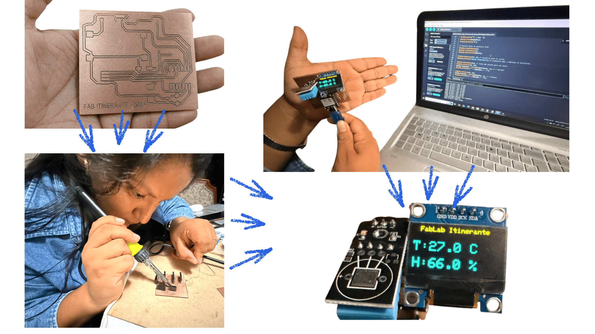
The soldering and assembly of the PCB board allowed for verification of the correct operation of the electronic circuit. During testing, the response of the components and the communication between the microcontroller, sensors, and display could be observed, confirming that the manufactured board operated properly..
Functional Testing
This board was developed and designed as part of the final project, with the objective of monitoring environmental variables in real time. The system measures temperature and humidity using the DHT11 sensor, as well as light intensity through an LDR sensor.
All the information collected by the sensors is processed by the XIAO ESP32-C3 and displayed through an OLED screen, allowing data visualization in a clear and immediate way. This integration creates a compact and interactive environmental monitoring system that combines sensors, data visualization, and electronic programming into a single board.
In addition, this project helped to understand the complete process of electronic design, PCB fabrication, component soldering, and functional system validation.
Components Used
| Component | Function |
|---|---|
| XIAO ESP32-C3 | Main microcontroller |
| DHT11 | Temperature and humidity sensor |
| LDR Sensor | Light intensity detection |
| OLED SSD1306 | Data visualization |
| Resistors | Electrical stability and control |
| Jumper Wires | Connections between components |
| USB-C | Power supply and programming |
Component Connections
DHT11 Sensor Connection
The DHT11 sensor is responsible for measuring environmental temperature and humidity.
| DHT11 Pin | Connection |
|---|---|
| VCC | 3.3V |
| GND | GND |
| DATA | GPIO 21 |
The sensor sends digital data directly to the ESP32-C3 for processing.
LDR Sensor Connection
The LDR sensor is used to detect the amount of ambient light.
| LDR Pin | Connection |
|---|---|
| One side | 3.3V |
| Other side | ESP32-C3 Analog Pin |
| Resistor | Connected to GND |
The LDR works by varying its resistance depending on the amount of light detected.
OLED SSD1306 Connection
The OLED display shows temperature, humidity, and light values in real time.
| OLED Pin | Connection |
|---|---|
| VCC | 3.3V |
| GND | GND |
| SDA | ESP32-C3 SDA |
| SCL | ESP32-C3 SCL |
Communication with the OLED display is performed through the I2C protocol.
General System Operation
- The DHT11 sensor captures temperature and humidity data.
- The LDR sensor detects ambient light intensity.
- The XIAO ESP32-C3 processes all sensor information.
- The data is sent to the OLED display.
- The serial monitor validates real-time readings.
System Validation
The ESP32-C3 board was tested together with the DHT11 sensor and OLED display to validate real-time temperature and humidity monitoring. The purpose of the test was to confirm correct communication between the microcontroller, the sensor, and the OLED display.
Serial Monitor Validation
During testing, the serial monitor correctly displayed temperature and humidity readings sent by the DHT11 sensor in real time.
Evidence Added:
- Serial monitor screenshots.
- Continuously updated data.
- Stable temperature and humidity readings.
Example Output:
Initialization complete.
Temp: 27.4 C | Hum: 74.0%
Temp: 27.5 C | Hum: 73.0%
Temp: 27.6 C | Hum: 74.0%
The serial monitor validated that the ESP32-C3 correctly receives and processes environmental data from the DHT11 sensor.
OLED Display Test
The OLED display was used to visualize temperature and humidity values in real time.
Evidence Added:
- Photograph of the OLED display turned on.
- Correct visualization of temperature and humidity values.
- Automatic data update every two seconds.
The OLED display correctly showed sensor data, allowing clear and stable visualization of environmental information.
Testing Procedure
- The ESP32-C3 board was connected through USB-C.
- The program was uploaded using Arduino IDE.
- The DHT11 sensor was connected to GPIO 21.
- Serial communication was initialized at 115200 baud.
- Temperature and humidity values were monitored through the serial monitor.
- The OLED display was validated by comparing displayed data with serial readings.
- Multiple tests were performed to verify system stability.
Hardware Used
| Component | Description |
|---|---|
| XIAO ESP32-C3 | Main microcontroller |
| DHT11 | Temperature and humidity sensor |
| OLED SSD1306 | OLED display |
| Arduino IDE | Programming environment |
Final Result
The system operated successfully by displaying stable temperature and humidity values on both the serial monitor and the OLED display. Communication between the ESP32-C3, DHT11 sensor, and SSD1306 display was successfully validated.
Programming
The following Arduino code was used to connect the XIAO ESP32-C3 with the DHT11 sensor and OLED display, allowing real-time temperature and humidity monitoring.
#include <Wire.h>
#include <Adafruit_GFX.h>
#include <Adafruit_SSD1306.h>
#include <DHT.h>

#define OLED_RESET -1
Adafruit_SSD1306 display(128, 64, &Wire, OLED_RESET);

const int DHTPIN = 21;
#define DHTTYPE DHT11

DHT dht(DHTPIN, DHTTYPE);

void setup() {

  Serial.begin(115200);

  Wire.begin();

  if(!display.begin(SSD1306_SWITCHCAPVCC, 0x3C)) {
    Serial.println(F("SSD1306 allocation failed"));
    for(;;);
  }

  display.display();
  delay(2000);
  display.clearDisplay();

  dht.begin();

  Serial.println("Initialization complete.");
}

void loop() {

  delay(2000);

  float humidity = dht.readHumidity();
  float temperatureC = dht.readTemperature();

  if (isnan(humidity) || isnan(temperatureC)) {

    Serial.println("Error reading DHT11 sensor.");

    display.clearDisplay();
    display.setCursor(0,0);
    display.print("Sensor Error!");
    display.display();

    return;
  }

  Serial.print("Temp: ");
  Serial.print(temperatureC);
  Serial.print(" C | Hum: ");
  Serial.print(humidity);
  Serial.println("%");

  display.clearDisplay();

  display.setTextSize(1);
  display.setTextColor(WHITE);
  display.setCursor(10, 0);
  display.println("FabLab Itinerante");

  display.setTextSize(2);

  display.setCursor(0, 20);
  String tempValue = String(temperatureC, 1);
  display.println("T:" + tempValue + " C");

  display.setCursor(0, 45);
  String humValue = String(humidity, 1);
  display.println("H:" + humValue + " %");

  display.display();
}
difficulties
The TT3018 CNC machine is not recommended for this type of work. Although different versions and quality levels exist, the unit I worked with exhibited constant connection problems and electrical noise, causing the machine to stop or disconnect during the machining process. According to my research, other users have also reported similar issues. Despite this, I made multiple attempts using Candle software to read and execute G-code, testing different configurations and reducing the complexity of the toolpaths; however, the problem persisted. Both individually and as a group, various solutions were attempted to resolve these issues, but the failures continued to appear during the process, preventing stable operation. One positive aspect worth highlighting is its height map calibration system, which allows for testing the Z-axis across the entire work area, proving especially useful for machining PCBs. However, despite various attempts and adjustments, the machine continued to malfunction, preventing the process from being completed properly. Therefore, the next step will be to use a different machine that guarantees greater stability and accuracy in order to fulfill the assignment.
Testing on the milling machine.
Reflection
On an individual level, this experience presented a significant challenge, as it involved learning new tools and overcoming technical difficulties during machining. Despite the problems encountered with the TT3018 CNC machine, I gained a deeper understanding of the complete PCB manufacturing workflow, from design in KiCad and Gerber file generation to processing in FlatCAM and preparing the G-code. This process also allowed me to develop analytical and problem-solving skills by experimenting with different configurations and alternatives to achieve a better result. Although the expected outcome wasn't achieved with this machine, the experience was valuable, as it reinforced my understanding of the process and the importance of having suitable and well-calibrated equipment. Finally, this stage provides me with a solid foundation to continue developing my final project, enabling me to make better technical decisions and optimize future electronic manufacturing processes.