Week 08 – Electronics Production

This week is focused on Electronics Production: understanding the in-house PCB production workflow, characterizing the milling process, preparing manufacturing files, producing a PCB, soldering the components, and testing an embedded microcontroller system that I designed.
On this page I document:
- The group assignment: characterizing the design rules for our in-house PCB production process.
- The workflow to submit a PCB design to a board house.
- My individual PCB design made in KiCad.
- The toolpath generation and PCB milling process.
- The stuffing, soldering and testing of the board.
- The problems I found and how I solved them.
Assignment and Learning Outcomes
The weekly assignment is:
- Group assignment:
- Characterize the design rules for your in-house PCB production process.
- Submit a PCB design to a board house.
- Individual assignment:
- Make and test an embedded microcontroller system that you designed.
- Extra credit: make it with another process.
Checklist
In this page I answer the required questions:
- Linked to the group assignment page.
- Documented how I made the toolpath.
- Documented how I made the board: milled, stuffed and soldered.
- Documented that my board is functional.
- Explained the problems and how I fixed them.
- Uploaded my source code.
- Included a hero shot of the board.
You can see the group documentation here:
Group Assignment – Characterizing the PCB Production Process

For the group assignment we characterized the design rules of our in-house PCB production workflow. The objective was to understand the real limitations of the milling process and identify the minimum trace width, spacing, tool diameter, and machine settings that produce reliable PCB results.
In our lab we worked with the PCB milling machine and used Mods CE to generate the toolpaths. In León the workflow is prepared for the MDX mill, while in Ponferrada the process is adapted to the Mono Fab workflow and VPanel.
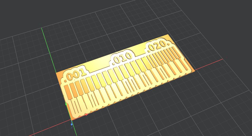
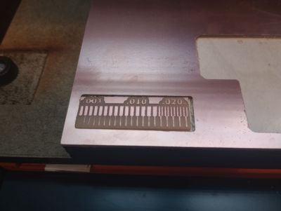
Test Files
We used the standard Fab Academy test files to evaluate the milling limits:
Machine and Tool
In our case we used a milling bit configured by default as 0.4 mm, which is an important reference for the trace width and clearance that can be manufactured safely. The reason is for have enougt resolution in the traces we need a small tool
- Software: Mods CE (mods.cba.mit.edu)
- Default milling diameter: 0.4 mm
- Important checks: machine origin, Z zero, speed, fixing of the tool, bed leveling
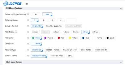
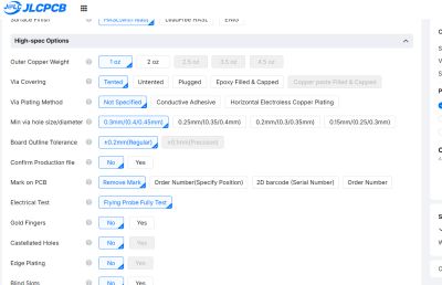
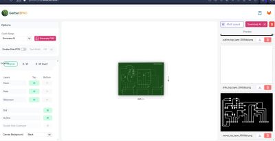
Workflow to Submit a PCB to a Board House
As part of the group assignment, we also documented the workflow to send a PCB design to an external board house such as JLCPCB or PCBWay. Even though my individual board was milled in-house, this workflow is useful for more complex designs or for boards requiring vias, solder mask, silkscreen or double-sided fabrication.
From KiCad to Gerber
- Finish the PCB design in KiCad.
- Run the design checks and verify the trace width and clearance.
- Open the Plot menu and export the Gerber files.
- Generate the drill files as well.
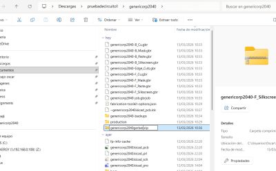
- Save all Gerbers and drills in a new folder.
- Compress the files into a ZIP file.
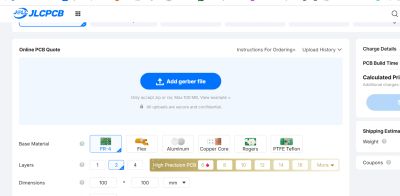
- open JLCPCB or PCBWay.
- Upload the ZIP file to a board house such as JLCPCB or PCBWay.
- Select options JLCPCB
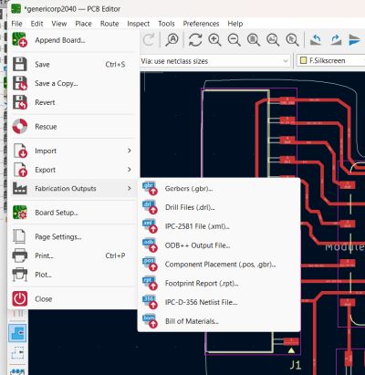
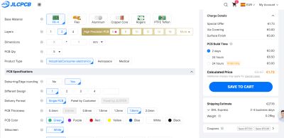
This process helped me understand the difference between manufacturing for in-house milling and manufacturing for industrial PCB fabrication.
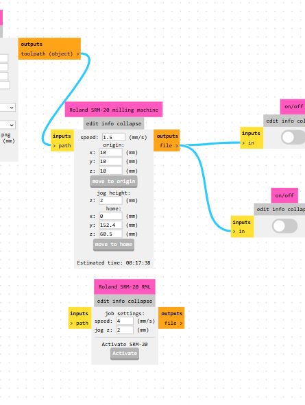
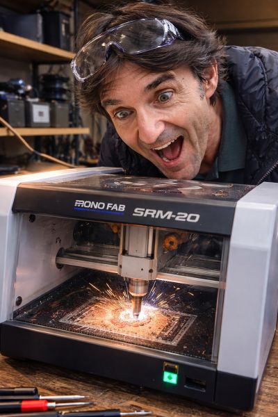
Roland MONO FAB SRM-20 – PCB Milling Workflow
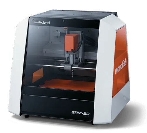
In our lab the PCB boards are milled using the Roland MONO FAB SRM-20. The workflow combines the use of Mods CE to generate the toolpaths and the VPanel SRM-20 software to control the machine. The following guide summarizes the process used to produce the PCB.
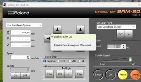
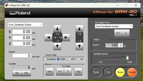
1. Connection and Initial Check
- Open the VPanel SRM-20 software.
- Verify that the computer detects the machine.
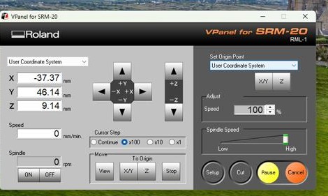
- Test the movement of the axes using the cursor controls.
- Move X or Y slightly to confirm the machine is responding.
- Important: be careful with the step value (Step x10).
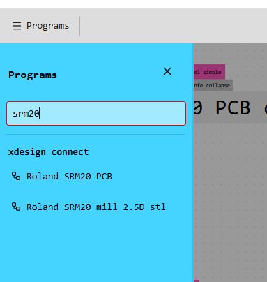
2. Computer Setup (Mods CE Project)
- Open the web browser and access Mods CE.
-
Load the program:
- Right click → Programs
- Open Program → Machines → Roland → Mono Fab → SRM-20 → Mill 2D PCB
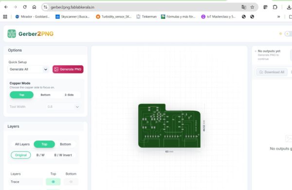
- Import the PCB file (PNG or SVG). You can do it dowloading the KICAD ZIP files in https://gerber2png.fablabkerala.in/
-
Image interpretation:
- White: copper
- Black: no copper
-
Trace configuration:
- Select PCB Defaults.
- Use a 0.4 mm milling bit (Mill Traces 1/64).
- Reduce the cutting speed to 2 mm/s (default value is higher).
3. Milling Parameters
The cutting speed depends on the milling tool diameter:
- 0.8 mm bit: 2 mm/s Used for the outline
- 0.4 mm bit: 1.5 mm/s Used for traces
- 0.3 mm bit: 1 mm/s By now we don´t use it
The machine parameters must also define:
- Origin coordinates (X,Y,Z)
- Jog height
- Home position
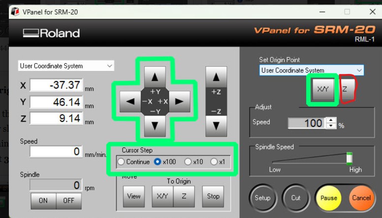
adjust zero x-y and z (red)
4. Generating the .RML File
- Activate the ON/OFF selectors in the output module.
- In the Mill Raster 2D module press Calculate.
- A preview window appears showing the milling toolpath.
- Check the path carefully.
- Save the generated .rml file.
5. Exterior Cut (Outline)
- Import the PNG file corresponding to the board outline.
-
Interpretation:
- White: material that remains
- Black: cutting path
- Select Mill Outline (1/32).
- Adjust the speed to 2 mm/s.
- Repeat the process: Calculate → Save .rml file.
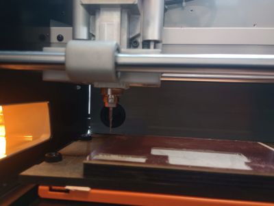
6. Preparing the Machine
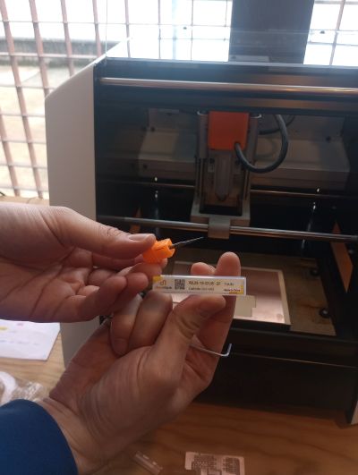
- Fix the PCB board on the sacrificial layer using double-sided tape.
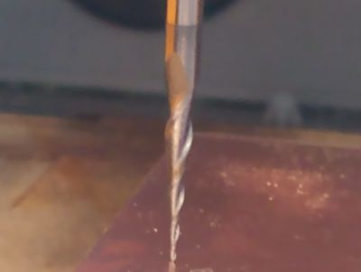
- Insert the 0.4 mm milling bit (traces) and tighten the screw.
- Only one person should manipulate the tool.
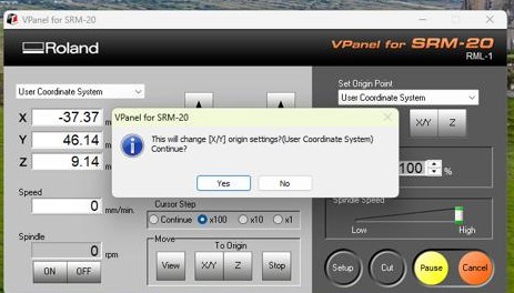
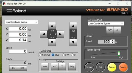
Setting the X and Y Origin
- Move the tool using the cursor.
- Press Set Origin Point.
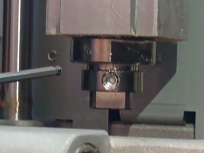
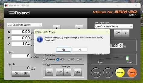
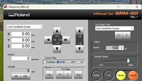
Setting the Z Origin
- Lower the Z axis close to the PCB surface.
- Loosen the screw slightly.
- Let the milling bit gently touch the board.
- Tighten the screw again.
- Press Set Origin Point Z.
- Raise the Z axis about 3 mm before starting.
Pics of the process
Initial web
Select machine
Charge png file
Set the cutting tool
Set the cutting speed
Results
7. Milling Process
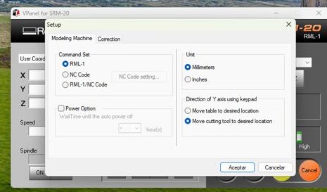
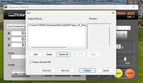
- Go to Setup → RML-1 → Millimeters.
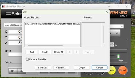
- Click Cut and load the .rml file.
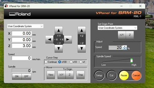
- Start with 20% speed for safety.
- Press Output to start the spindle.
- If everything is correct, increase to 100% speed.
Once the traces are finished, clean the dust and change the tool to the 0.8 mm bit for the outline cut. The Z origin must be adjusted again, but the X and Y origin remain the same.
What We Learned
- The real milling limits are not only defined by the design software, but also by tool wear, machine calibration, and bed leveling.
- The 0.4 mm tool sets practical limits for trace width and clearance.
- A correct Z origin is critical: if it is too low, the copper is overmilled; if it is too high, traces are not isolated correctly.
- Bed leveling strongly affects the quality of PCB isolation.
- Open pins and accessible headers are very useful for later debugging and for future assignments.
I also learned that PCB production requires attention not only in the design stage, but also in the manufacturing setup. Small errors in tool height, origin or tool fixing can easily ruin a board.
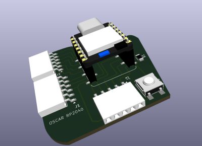
Individual Assignment – Embedded Microcontroller System
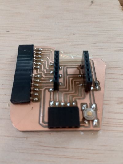
For the individual assignment I designed and fabricated my own embedded microcontroller board. The board was created in KiCad, prepared for milling, manufactured on the PCB mill, populated with components, soldered by hand, and finally tested to confirm that it works correctly.
Before finalizing the design, I checked that the PCB was ready for milling:
- Trace width prepared for the in-house process.
- Minimum spacing adapted to the milling limitations.
- Open pins / headers added for debugging and future assignments.
- Component placement reviewed to simplify soldering.
The goal was not only to draw a PCB, but to complete the full workflow: design + export + toolpath + milling + stuffing + soldering + programming + testing.
you can see the electronic design week here to see the projectPCB Design in KiCad
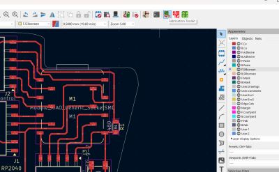
Schematic Design
I started by creating the schematic of the board in KiCad. The design includes the microcontroller, programming connections, power routing, and the input/output elements required for my board functionality.
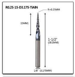
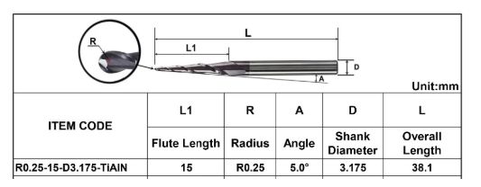
- Microcontroller: XIAO RP2040
- Power section: USB
- Input-output: button, connectors
- Open headers: added for future connections and debugging
PCB Layout
After the schematic, I moved to the PCB editor to place the components and route all traces. During this step I paid special attention to the trace width and spacing required by our in-house milling process.
- I kept the routing as clear and simple as possible.
- I checked that no traces were too close for the 0.4 mm milling process.
- I left enough space around pads to improve soldering reliability.
- I included accessible pins for future testing and expansions.
Preparing the Manufacturing Files
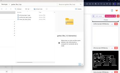
For the in-house milling workflow, I exported the PCB project from KiCad and converted it into PNG files suitable for Mods CE.
Gerber to PNG
I used the Gerber to PNG workflow to obtain the monochrome files needed by Mods:
- Traces PNG for copper isolation
- Outline PNG for cutting the final board contour
The conversion can be done using: Kerala fab lab
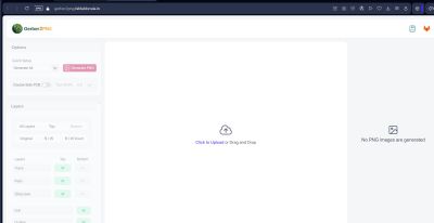
Upload the files, we can use ZIP files
Upload jpg files
This was the steps:
- Export Gerbers from KiCad.
- Import the Gerber files into the converter.
- Generate black and white traces and outline PNG files.
- Download the generated images.
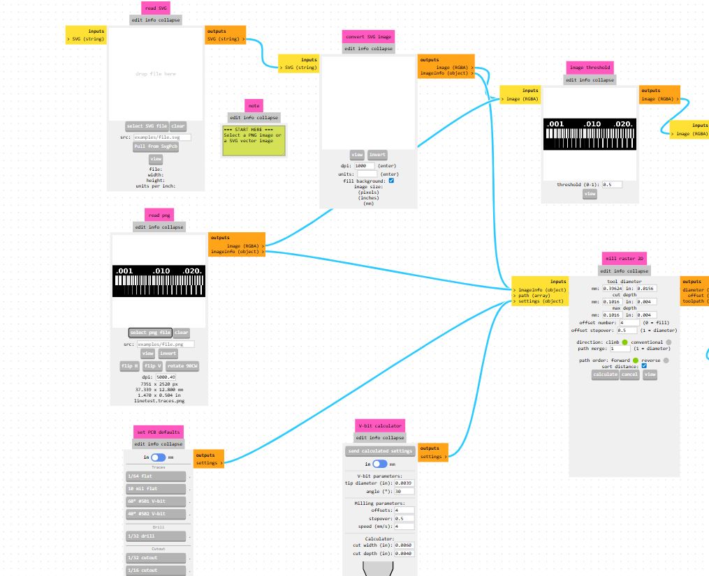
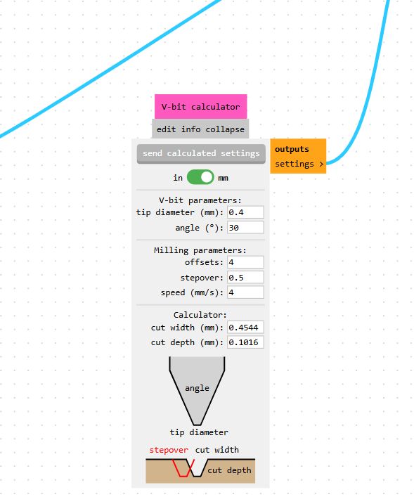
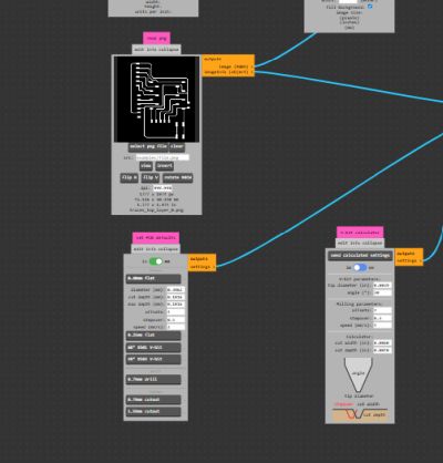
Toolpath Generation in Mods CE
Once I had the PNG files, I imported them into Mods CE to create the toolpaths for PCB milling. This is the stage where the machine instructions are generated based on the traces and outline images.
Toolpath Workflow
- Open Mods CE.
- Load the traces PNG.
- Select the proper machine program.
- Configure the milling parameters.
- Generate the toolpath for the traces.
- Repeat the process for the outline PNG.
- Export the files for the milling machine.
Important Parameters
- Tool diameter: 0.4 mm
- Cut depth: adjusted for copper isolation
- Max depth: adapted for board cutting
- Offsets: defined to isolate traces correctly
- Origin: checked carefully before milling
The new File
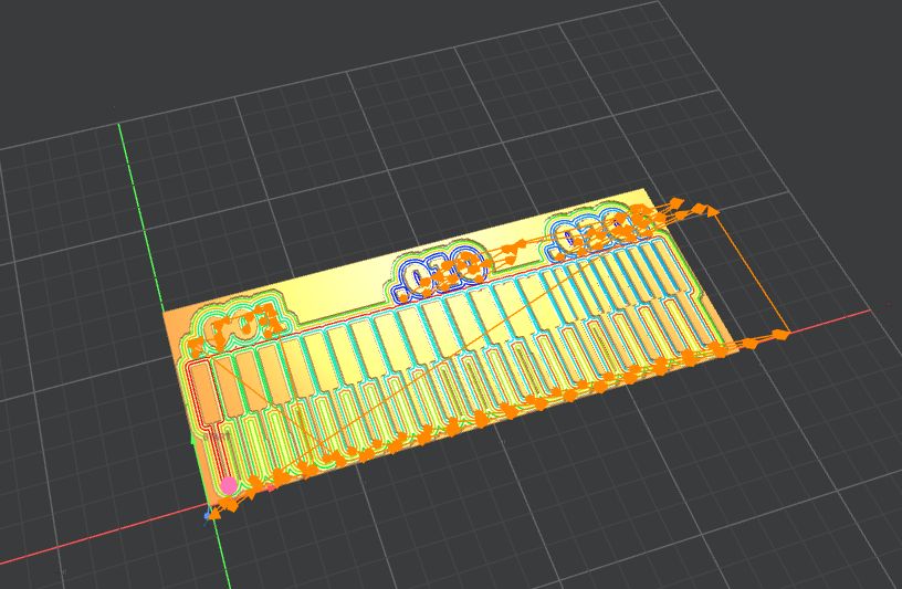
Set the cutting speed
General vision of the process
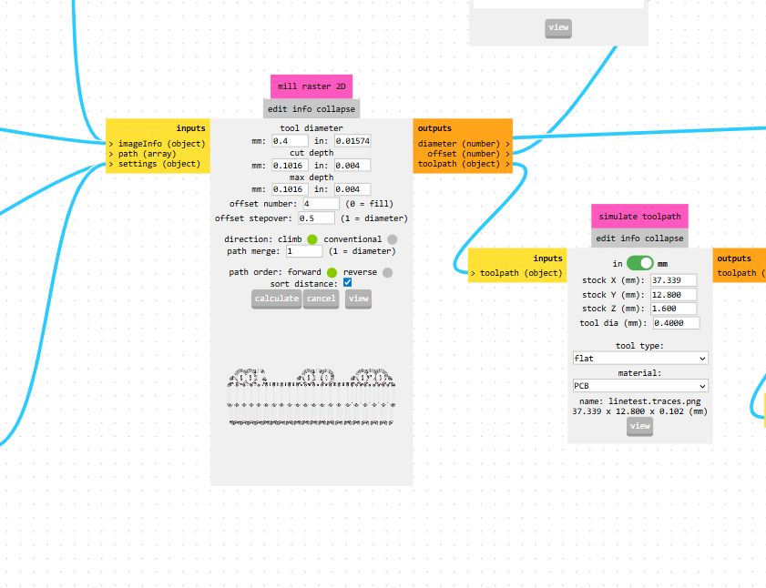
This part was very important because a correct toolpath determines whether the board can be milled successfully or not.
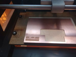
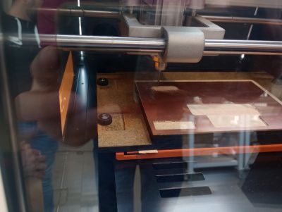
PCB Milling Process
After preparing the toolpaths, I moved to the milling machine to fabricate the PCB. I first milled the traces and then cut the outline.
Machine Setup
- Fix the PCB material on the machine bed.
- Insert and tighten the milling bit carefully.
- Set the X, Y and Z origin.
- Check the bed leveling.
- Load the traces file and start milling.
- Change to the outline process after checking the traces.
Important Notes
- Special care is needed when setting the Z height.
- The tool must be fixed correctly to avoid breakage.
- The machine should be controlled by only one person.
- In Ponferrada, I used a small vacuum cleaner and brush to clean the board and remove debris.
- A small ruler helped me check positioning during setup.
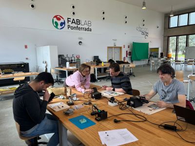
Here we had the previous group project before starting the individual one
Select the cut tool and instal in machine
Start the VPanel
Adjust X,Y and Z axis
In the VPanel
The axes are correctly positioned and selected. Now we need to raise the cutting tool to prevent it from starting on the board. At the same time, we select a lower starting speed of 20%, which we will later adjust once the process begins in case there are any problems with the milling.
Now we delete the previous programs and load the milling programs, first the one for the tracks and then the one for the cutting
Start the work "output" button
Finnal result
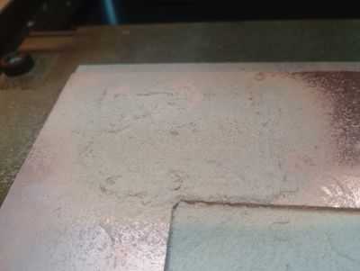
Machine leveling problem
During the PCB milling process we observed an inconsistency in the depth of the traces. In some areas the copper was completely removed while in others the milling bit only scratched the surface.
This behavior indicates that the PCB surface was not perfectly parallel to the milling plane of the machine. This can happen due to:
- Uneven sacrificial layer
- PCB board not properly fixed
- Incorrect Z calibration

To mitigate the problem Nuria and Adrian reattached the PCB board, recalibrated the Z origin and verified the surface flatness before running the job again. this are his notes
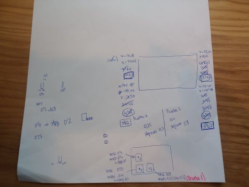
As you can see in the notes, it was necessary to adjust the position of the Z axis many times to check the leveling, and in the future it will be necessary to use the middle of the board to calibrate the Z axis
Finally this is the result
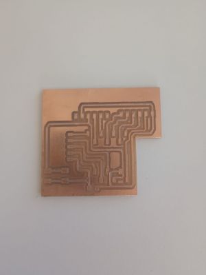
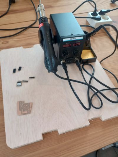
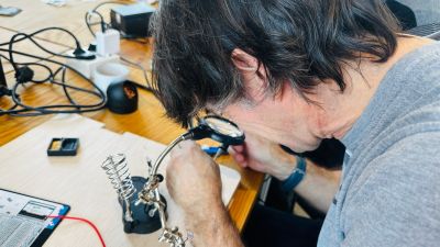
Stuffing and Soldering the Board
Once the board was milled, I prepared all the electronic components and soldered them manually. This was a delicate step because the board contains small pads and components, so clean soldering technique was important.
Tools and Materials
- Fine tip soldering iron
- Thin solder wire
- Flux
- Tweezers
- Brush and cleaning tools
I used the Fab Academy soldering references and debugging slides to improve the assembly process.
Assembly Process
- Clean the PCB after milling.
- Organize the components by value and package.
- Solder the smallest SMD components first.
- Continue with connectors, headers and larger parts.
- Check component orientation carefully, especially LED polarity.
- Inspect the board for shorts, cold joints or missing connections.
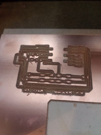
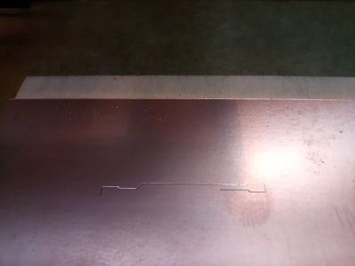
Trace spacing problem
During the PCB milling process we detected that two traces were placed too close together. Because the spacing was smaller than the diameter of the milling bit, the tool could not remove the copper between them.
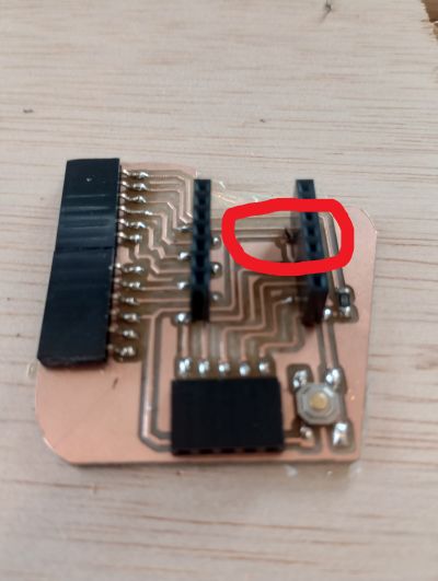
As a result, a small copper bridge remained connecting both traces.
To fix the problem we carefully removed the copper bridge using a cutter blade and then resoldered the affected area to restore the correct electrical separation.
Testing and Functionality
After soldering, I tested the board to confirm that the microcontroller system was functional. I checked power continuity, programming connection, and the operation of the board features.
- I visually inspected all solder joints.
- I checked for shorts between power and ground.
- I connected the board to the programmer.
- I uploaded the firmware successfully.
- I verified that the board performs the intended function.
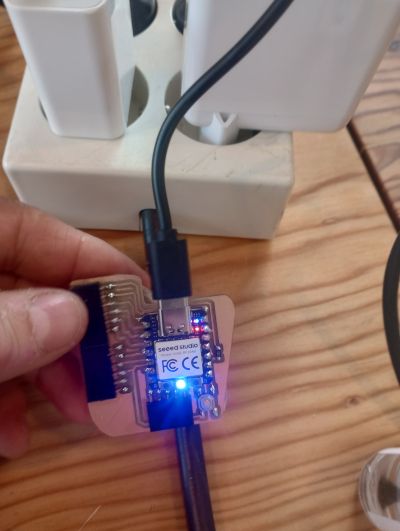
The board is functional When the button is pressed, the onboard LED is activated. This is a simple test program used to verify that the board is working correctly. “the LED blinks”, “the button changes the LED state”,
Problems and Fixes

Problem 1 – Machine Leveling
- Problem: During the milling process the traces were not milled uniformly. In some areas the copper was removed correctly, while in others the milling bit barely touched the surface. This indicated that the PCB was not perfectly leveled relative to the milling plane.
- Fix: This issue was solved with the help of Nuria and Adrián. They worked on adjusting the machine by replacing the sacrificial layer and adding cardboard washers to compensate for small height differences. After several tests and adjustments the machine was properly leveled. This process required several hours of work.
Problem 2 – Trace Spacing
- Problem: Two traces in the PCB design were too close together. Because the spacing was smaller than the diameter of the milling bit, the machine was unable to remove the copper between them, leaving a small copper bridge connecting both traces.
- Fix: I solved this issue manually by carefully cutting the unwanted copper bridge with a cutter and then resoldering the affected connections to restore the correct electrical paths.
Problem 3 – Soldering Difficulties
- Problem: Some connections required extra attention during soldering, especially after fixing the trace spacing issue.
- Fix: I carefully cleaned the solder joints and resoldered the connections to ensure proper electrical contact.
Solving these problems required many hours of work, including machine adjustments, PCB remilling attempts, and manual corrections during soldering. Although it was time-consuming, the troubleshooting process helped me better understand the importance of machine calibration, proper PCB design spacing, and careful assembly.
Design Files, Source Code and Hero Shot
Design Files
Source Code
Summary and Reflection

This week helped me understand the complete workflow of electronics production, from PCB design in KiCad to file export, toolpath generation, milling, soldering, programming and testing.
During this assignment I also experienced several real manufacturing problems. The most important one was related to machine leveling. The PCB surface was not perfectly aligned with the milling plane, which caused inconsistent milling depth across the board.
This issue required several hours of adjustments. With the help of Nuria and Adrián, the machine was recalibrated by replacing the sacrificial layer and adding cardboard washers to compensate for small height differences. After several tests the milling surface was finally leveled correctly.
Another issue appeared in the PCB itself when two traces were too close together. Because the spacing was smaller than the milling bit diameter, the machine could not remove the copper between them and a small bridge remained. I solved this problem manually by cutting the unwanted copper trace and resoldering the affected connections.
Overall, I invested many hours solving these issues, but the process helped me understand the real limitations of PCB milling and the importance of proper machine calibration, correct trace spacing, and careful debugging.
The final result was a functional microcontroller board, and despite the challenges, this assignment gave me much more confidence in producing my own custom electronics for future Fab Academy work.