Week 06 – Electronics Design

This week is focused on Electronics Design: using an EDA tool to design a development board, checking that it can be fabricated, and using lab test equipment (including a logic analyzer) to observe the operation of a microcontroller circuit.
On this page I document:
- The group assignment: observing a microcontroller circuit with lab test equipment and a logic analyzer.
- My electronics design workflow using KiCad and the Fab Academy libraries.
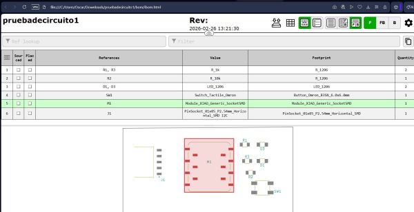
- The development board I designed around a Seeed XIAO RP2040 with a pin header, one button, and two LEDs.
- An additional connector-only board that breaks out the XIAO RP2040 pins.
Assignment and Learning Outcomes
The weekly assignment is:
- Group assignment:
- Use the test equipment in the lab to observe the operation of a microcontroller circuit board.
- As a minimum, demonstrate the use of a logic analyzer.
- Document the work on the group work page and reflect on the individual page.
- Individual assignment:
- Use an EDA tool to design a development board that uses parts from the inventory.
- The board must interact (local input &/or output) and communicate with an embedded microcontroller.
The learning outcomes are:
- Select and use software for circuit board design.
- Demonstrate workflows used in circuit board design.
- Design a development board that interacts with and communicates with a microcontroller.
Checklist
In this page I answer the required questions:
- Linked to the group assignment page.
- Documented what I learned in electronics design.
- Checked that my board can be fabricated.
- Explained problems and how I fixed them.
- Included the original design files (KiCad, etc.).
- Included a hero shot of the final board.
You can see the group documentation here:
Group Assignment – Microcontroller Board Measurement
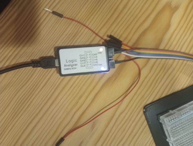
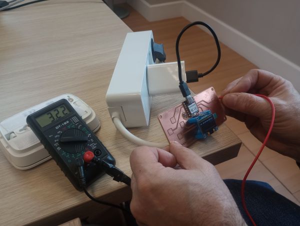
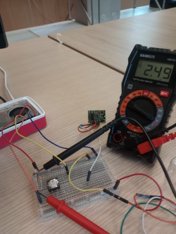
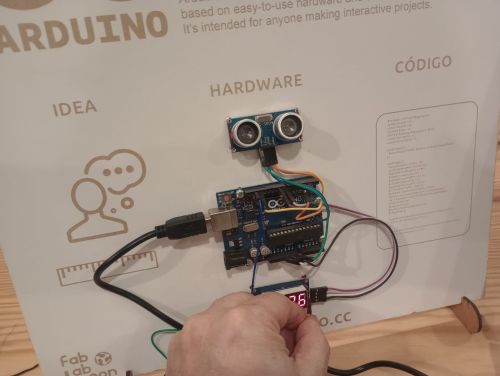
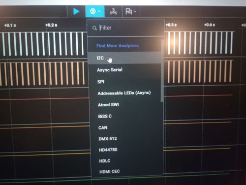
For the group assignment we used the lab’s test equipment to observe the behaviour of a microcontroller circuit board. The goal was to capture and analyze digital signals, and at minimum, to demonstrate the use of a logic analyzer.
Test Equipment Used
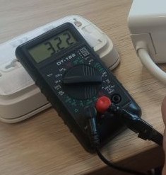
- Bench power supply (5V / 3.3V).
- Logic analyzer (USB, connected to a PC).
- Microcontroller development board (with LED blink + UART firmware).
- I2C adapter and jumper wires.
Signals Observed
We focused on two types of signals:
- GPIO pin connected to an on-board LED blink test.
- I2C pin used for communication.
Measurement Procedure
- Powered the board and uploaded a simple test program (LED blinking ).
- Connected the multimeter ground to the board GND.
- Connected one multimeter channel to the LED GPIO and another to the resistance.
- Configured the sampling rate and voltage threshold in the multimeter
- View the results
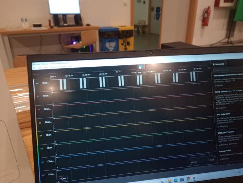
Measurement Procedure for analyzer
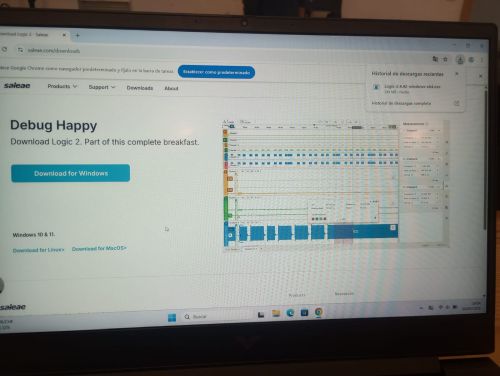
- Upload the analyzer program Descargar Saleae
- Powered the board and uploaded test program and I2C conmunication
- Connected the logic analyzer ground to the board GND.
- Connected one logic analyzer channel to the LED GPIO and another to the IC2 pin.
- Configured the sampling rate and voltage threshold in the logic analyzer software.
- Triggered a capture while the board was running.
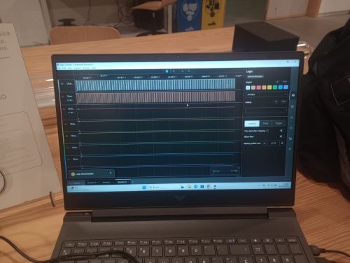
Observations and Learnings
- The LED GPIO signal showed a clean square wave, and we confirmed the blink period matched the code.
- The I2C signal decode matched the configured baud rate and transmitted characters.
- We saw how timing issues or wrong baud rate settings can be diagnosed using the logic analyzer.
- Ground reference and wiring quality have a clear impact on signal integrity and noise.
Working with the logic analyzer made it much easier to understand what the microcontroller was actually doing “on the pins”, instead of treating the board as a black box.
Individual Assignment – Development Board Design
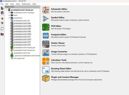
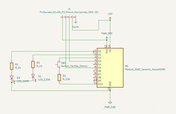
For my individual assignment I used KiCad (with the Fab Academy libraries) to design a small development board built around a Seeed XIAO RP2040.
The design includes:
- A pair of pin header connectors to plug in the XIAO RP2040 module.
- One push button connected to a GPIO (local input).
- Two LEDs with current-limiting resistors, each connected to a GPIO (local outputs).
- An additional small board that only includes connectors to break out the XIAO RP2040 pins.
This satisfies the requirement to design a development board that can interact (button + LEDs) and communicate with an embedded microcontroller (the XIAO RP2040 module).
EDA Toolchain and Workflow
Software and Libraries
- KiCad – schematic and PCB layout.
- Fab Academy KiCad libraries – symbols and footprints compatible with the Fab inventory.
- Mods – to generate toolpaths and visually verify the traces for milling.
Workflow Overview
- Create a new KiCad project for Week 06.
- Draw the schematic from scratch, using Fab library components.
- Assign footprints and configure the board stackup.
- Do the PCB layout and routing, respecting the milling design rules.
- Run ERC/DRC and fix all issues.
- Export manufacturing files and simulate the milling in Mods.
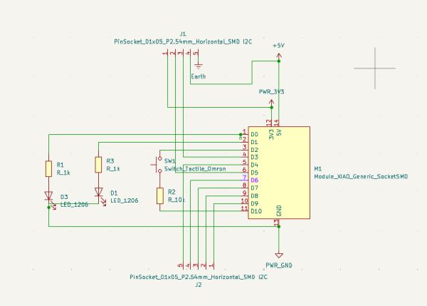
Schematic Design – XIAO RP2040 Development Board
Main Components
- XIAO RP2040 (as a 2×7 or 2×8 pin header footprint, depending on the module).
- Push button (momentary, normally open) with pull-up or pull-down resistor.
- LED1 + series resistor (e.g. 499 Ω) connected to GPIO.
- LED2 + series resistor connected to another GPIO.
- Pin header for power and future external connections.
Connections
- The XIAO RP2040 module provides 3.3V and GND rails to the board.
- The button is wired between GPIO and GND, with a pull-up (internal or external).
- Each LED is connected from GPIO → resistor → LED → GND (active-high configuration).
- Additional header pins break out free GPIOs and power for future sensors or communication interfaces.
The schematic was completed and then checked with KiCad’s Electrical Rules Check (ERC) to make sure all power pins were driven, no unconnected pins remained, and there were no obvious shorts.
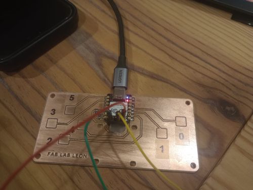
Additional Board – more connectors
In addition to the main development board, I designed a very simple second PCB that includes connectors for all pins for the XIAO RP2040 The goal of this board is to:
- Provide a clean mechanical support for the module.
- Break out all pins to 2.54 mm headers for breadboard or jumper wire use.
- Allow re-use of the same microcontroller module for other experiments.
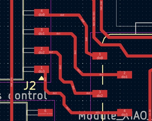
This board has one connector for I2C – 2 leds - one button one connector for the rest of the pins- headers and the XIAO RP2040 footprint – but it follows the same KiCad workflow and milling constraints as the main board.
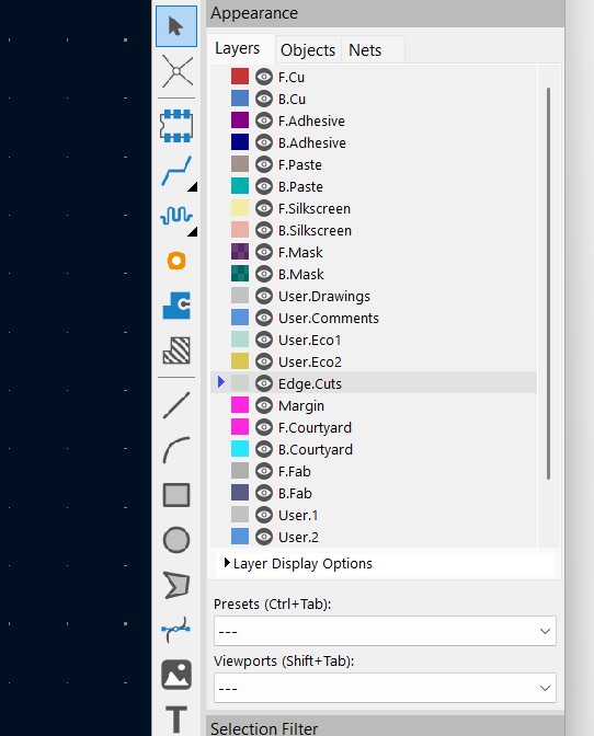
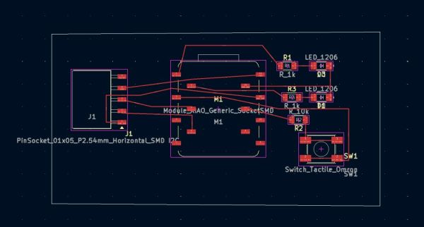
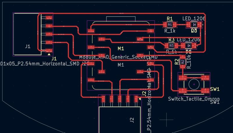
PCB Layout and Routing
Board Outline and Component Placement
- Small board sized to the XIAO RP2040 footprint with a bit of extra margin.
- The XIAO headers are placed near the center for stability.
- The button is located at one edge for easy access with a finger.
- The LEDs are placed near the top side so they are clearly visible in the hero shot.
- The connectors - in two sides.
Routing Strategy
- Single-sided routing (top layer) compatible with PCB milling in the Fab lab.
- Trace width and clearance selected according to the standard Fab design rules (e.g. 0.4 mm / 0.4 mm).
- Short direct routes from GPIO pins to LEDs and button to minimize complexity.
- Use of ground lines around the board to simplify connections and reduce noise.
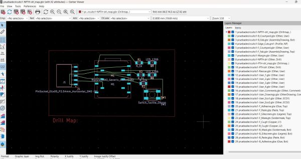
Fabrication Check
The Fab Academy FAQ explains that if the EDA tool does not include a complete DRC for our milling process, we can still verify the design by generating toolpaths and inspecting them.
Steps Taken
- Exported the traces and outline from KiCad as Gerber or SVG files.
- Loaded the files into Mods and selected the appropriate tool (e.g. 1/64" end mill).
- Generated the isolation toolpaths for traces and the cutout path for the outline.
- Visually inspected the result to check:
- That all traces were isolated (no accidental shorts).
- That no traces were thinner than the tool could handle.
- That pads had enough copper around them for soldering.
After this inspection I confirmed that the board can be fabricated with the milling process available in the lab.
Problems and Fixes
Footprint and Orientation Issues
- Problem: Initially I selected a header footprint that didn’t perfectly match the XIAO RP2040 pin spacing.
- Fix: I switched to the correct footprint from the Fab library and re-aligned the module.
Clearance Too Small
- Problem: Some traces were routed too close together for the milling bit diameter.
- Fix: I updated the KiCad design rules (trace width and clearance) and re-routed the critical nets.
LED Polarity
- Problem: In the first version the LED polarity was reversed in the footprint.
- Fix: I double-checked the LED footprint and symbol, corrected the orientation in the PCB, and updated the silkscreen marks.
These issues were caught before fabrication thanks to ERC/DRC and visual inspection in 3D view and Mods.
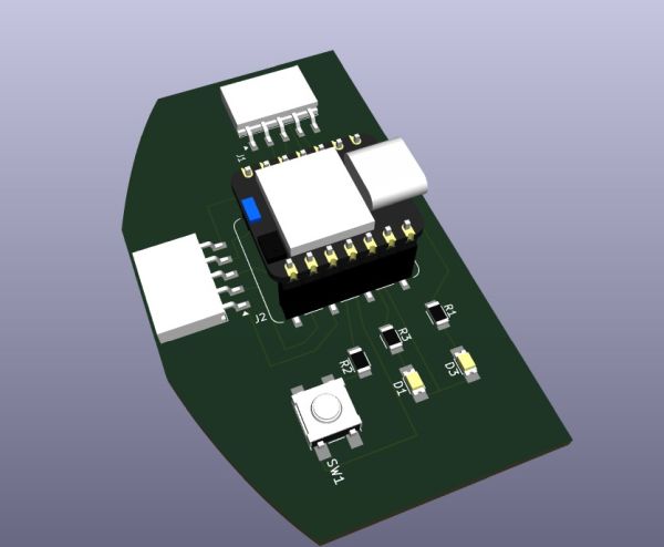
Design Files and Hero Shot
Original Design Files
- KiCad project – XIAO RP2040 development board
- KiCad project – XIAO RP2040 connector-only breakout
- Gerber files – development board
Original Design Files version 2
Original Design Files generic version
- KiCad project – generic XIAO RP2040 development board
- KiCad project – generic XIAO RP2040 connector-only breakout
- KiCad project – generic XIAO RP2040 PCB
Original Design Files color sensor version
- KiCad project – color XIAO RP2040 development board
- KiCad project – color XIAO RP2040 connector-only breakout
- KiCad project – color XIAO RP2040 PCB
Summary and Reflection
This week connected EDA tools, design rules, and real fabrication constraints. Starting from a blank KiCad project and designing the board from scratch helped me understand every step of the electronics design workflow: schematic capture, footprint selection, PCB layout, DRC, and fabrication checks.
By designing a simple but complete development board for the XIAO RP2040 (button + two LEDs + connectors) I met the requirement of creating hardware that can interact and communicate with an embedded microcontroller. The extra connector-only board will make it easier to reuse the microcontroller in future assignments.
Measuring signals with the logic analyzer closed the loop between design and debugging: I could see the digital behaviour of the system and verify that the hardware and firmware were working together as intended.