Week6 Electronic Design.
INTRODUCTION
We start the sixth week, and we are tasked with designing an electronic board. Obviously, for this, we need PCB design software and to learn how to use it. At the same time, certain knowledge of electricity and electronics must also be acquired if not already known.
To familiarize ourselves with the world of electricity and electronics, in the group assignment we will work together with various measuring instruments, taking readings from different electronic devices. This will allow those who are not used to these quantities to get in touch with them. Fortunately, in my case, I must say that I already have experience in this area, especially in electricity, though less so in electronics. To better understand how an electrical circuit works, we will use, in the individual assignment, several simulation programs. Finally, the main challenge will be to design a development electronic board using a design program for this purpose (EDA).
GROUP ASSIGNMENT
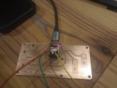
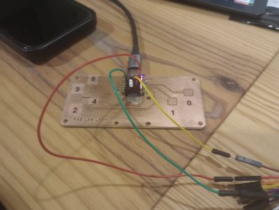
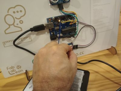
FabLab Leon work groupThis week’s group assignment involved working with a multimeter, oscilloscope, and a logic analyzer.
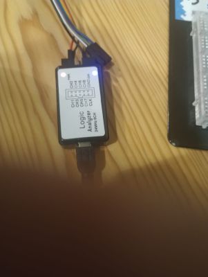
I already have experience in this area because I work daily with these instruments, except for the logic analyzer, which I did not know before but really enjoyed. I have even ordered one for future use.
MULTIMETER
Measuring resistances in series, parallel, or combined circuits is routine in my work, as is checking continuity, capacitor values, or voltages. In my case, the difference is that I usually work with medium voltage circuits, single-phase 220V, three-phase 380V, and sometimes bifilar or three-phase 220V circuits.
Some important points when using a multimeter:
- To measure resistance/continuity/LED, the circuit must be open and de-energized, measuring across the element(s).
- To measure voltage, the circuit must be powered, and measurements are always taken in parallel across the element(s).
- To measure current, the multimeter must be in series with the circuit. Be careful to set the range above the expected current; exceeding the meter’s rating can blow its fuse or damage the multimeter.
- To measure capacitance, always ensure the capacitor is isolated from the circuit and discharged.
OSCILLOSCOPE AND LOGIC ANALYZER
Working with oscilloscopes is very useful in electronics, though my experience has mostly been with AC currents in rectifiers, inverters, variable drives, and other frequency-altering devices.
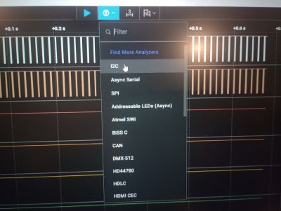
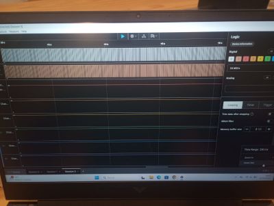
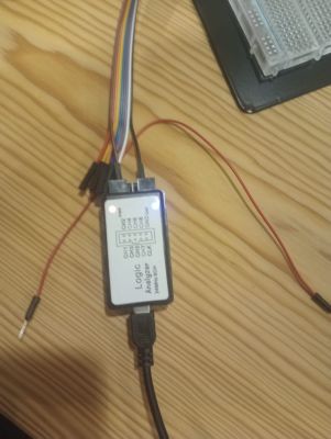
For electronics work, I preferred the logic analyzer, which, although similar to an oscilloscope, allows multiple channels and better measurement adjustments. You can clearly see communication patterns between components and how they change according to commands sent to the controller.
I2C
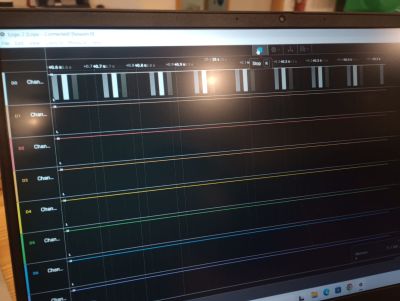
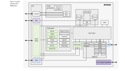
For testing purposes, the logic analyzer was interfaced with the I2C bus of the RP2040. By probing the SDA and SCL lines, usually connected to the OLED display, we can monitor the data frames and clock signals responsible for generating the visual output.
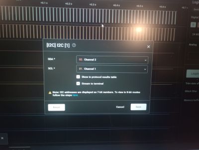
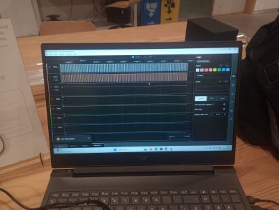
While we are still scratching the surface of protocol decoding, identifying these patterns is the first step toward fully understanding bus communications. One step at a time!
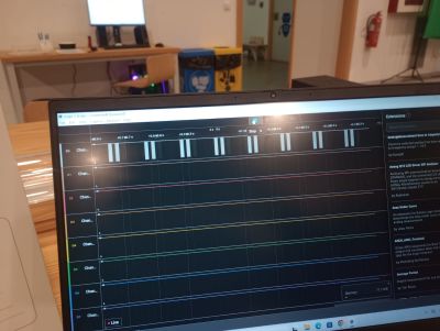
LED Display
We subsequently repeated the test with a standard LED display to analyze the simpler signal patterns used to drive numeric segments compared to the previous OLED setup.
INDIVIDUAL ASSIGNMENT
The first part of the individual assignment is to simulate an electronic circuit using online programs. In my case, I chose two tools: Wokwi and Falstad Circuit Simulator.
Wokwi
A very interesting tool, as it allows simulating the operation of different controllers, creating your own electronic circuit, and verifying its functionality.
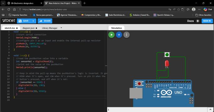
I chose the Arduino Uno, the only one familiar to me thanks to the Embedded Programming assignment. Here, I copied a simple Arduino code as a test to control an LED with a push button. The result was very interesting: I could see the LED working when pressing the button, and I could also see voltage changes on an oscilloscope.
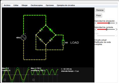
Falstad
In my opinion, this tool is more basic, but more focused on learning than experimentation. The previous tool allows you to verify if a model is functional before physically testing it, thus avoiding damage to real components in case of a severe design error.
This tool, on the other hand, allows you to draw more or less basic circuits and see and understand how current flows through the various components. For example, you can observe how a capacitor charges and discharges, see the current through an inductor, and how the current intensity varies depending on voltage or resistances introduced, or observe the paths the current takes when switching elements and other components. However, it should also be noted that sometimes what we see are errors: if we force shorts or other mistakes, the program may not simulate correctly, although it will indicate that there are incorrect connections.
EDA
Once we have worked with the simulation tools mentioned above, it is time to design a development board.
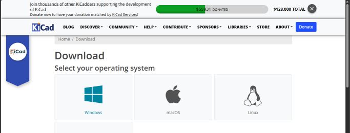
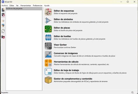
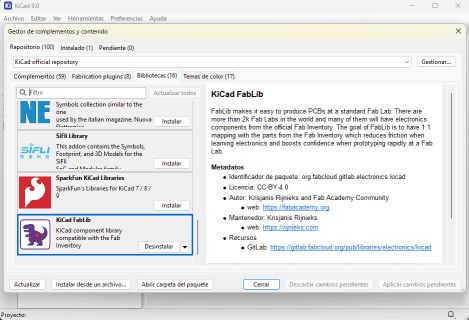
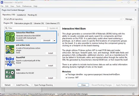
For this, the first step was to download an EDA program on my computer, in this case KiCad 9.0. Once installed, I also had to download the FAB libraries to use the same components available in the FabLab. Additionally, based on my tutors’ recommendations, I downloaded the BOM plugin to generate, once the design is finished, a web page summarizing all the components used.
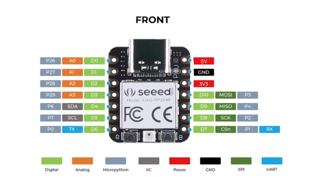
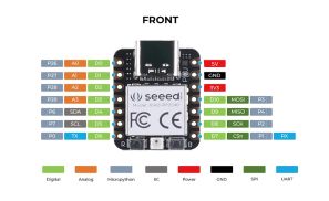
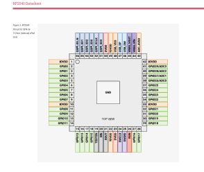
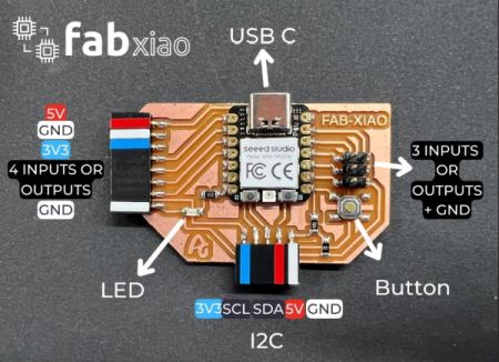
Of course, considering that we are going to use a >Seeed Studio XIAO RP2040 as the controller, it is very important to know the pinout of this component.
KICAD
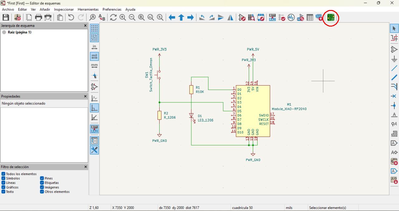
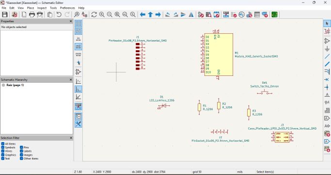
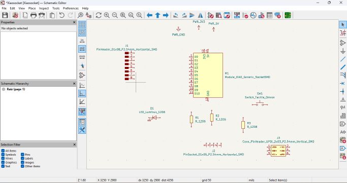
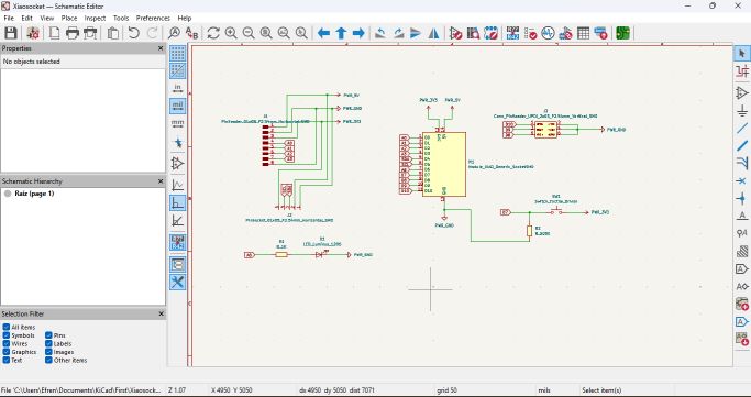
Once I had KiCad installed and configured, I began designing a board. First, I tried to copy the example provided by my tutors following Neil’s class recommendations. Gradually, I got used to KiCad’s interface, how to obtain the necessary elements from the libraries, and how to draw them in the schematic. Using labels helped me place the connections correctly.
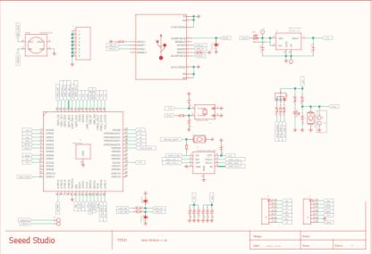
One question I had was how to find the necessary components in the FabLab inventory. To address this, I used the BOM that Adrian created on his website.
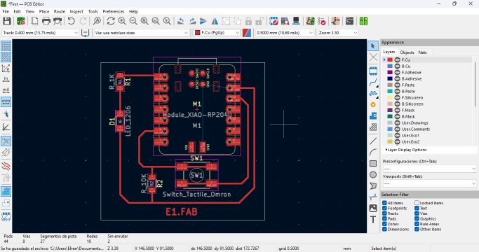
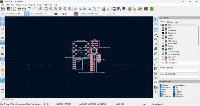
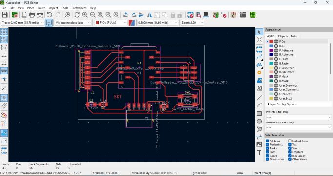
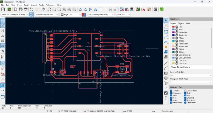
Once the schematic was complete, I moved on to editing the board itself and placing the traces—the most difficult part, surprisingly—since traces must be routed without crossing. There are some tricks, such as using a 0Ω resistor, but I tried to avoid using it.
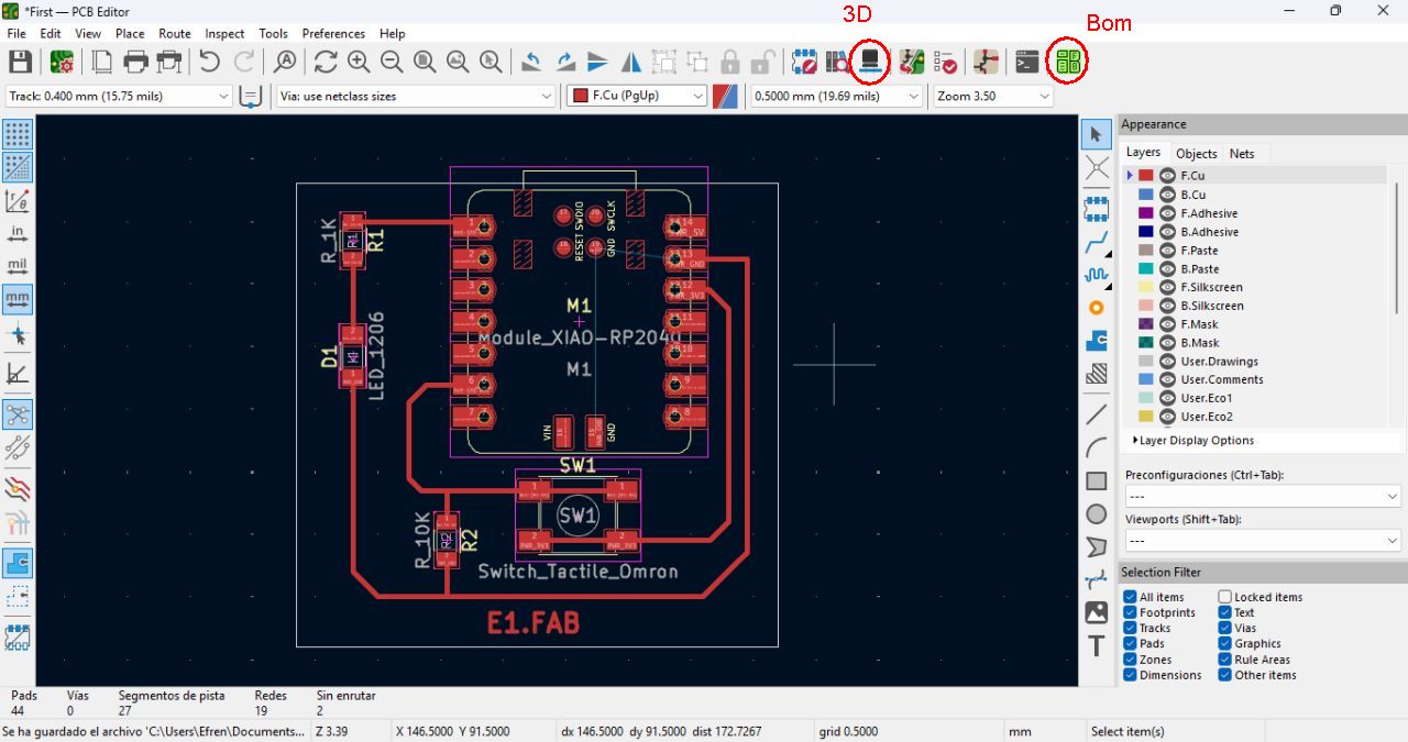
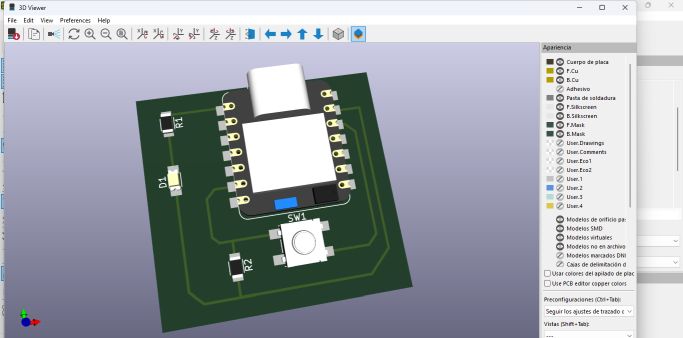
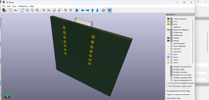
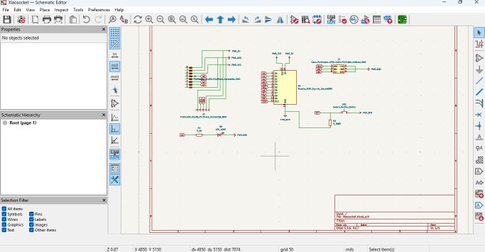
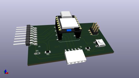
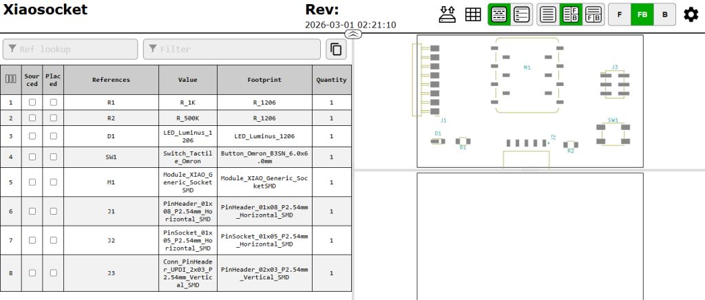
After completing the design and finalizing the PCB with the cut line, I generated a 3D view and created my first BOM.
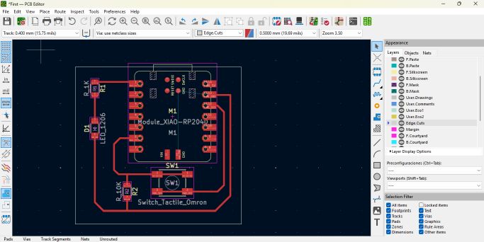
MY FIRST PCB
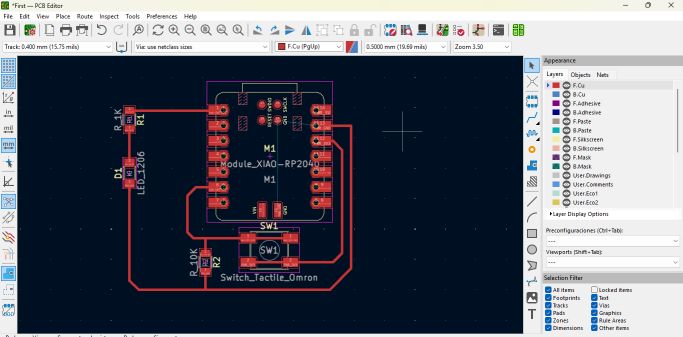
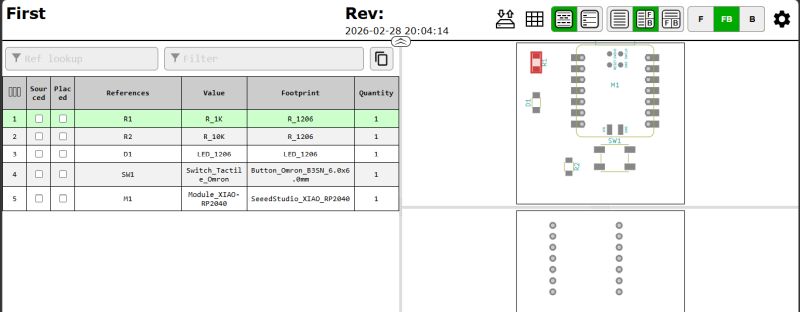
Next, I created the PCB required for the assignment: a board with an RP2040 controller mounted on sockets so it can be inserted and removed, a LED, a push button, and exposed pins. Using the provided image and BOM as reference, I got to work.
A beginner mistake I made was placing the 8-pin connector upside down, which I realized while editing the PCB because the connections ended up completely crossed.
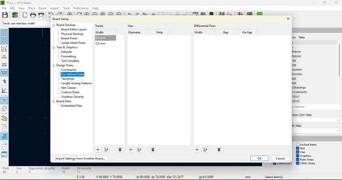
Another important point: whenever starting to draw traces on a PCB, you must select the trace width; the default is 0.4 mm.
One of my goals was to avoid using a 0Ω resistor as in the example, which I achieved by using the space between the connector pins.
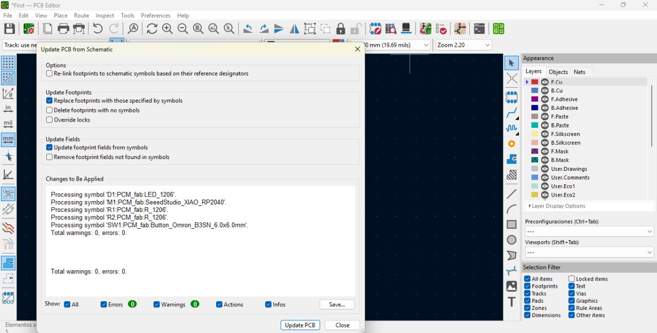
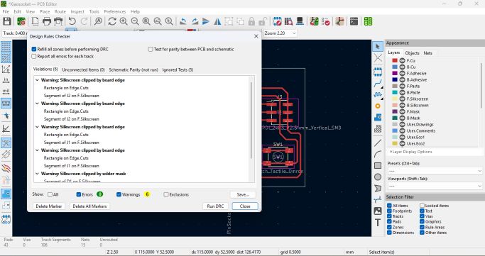
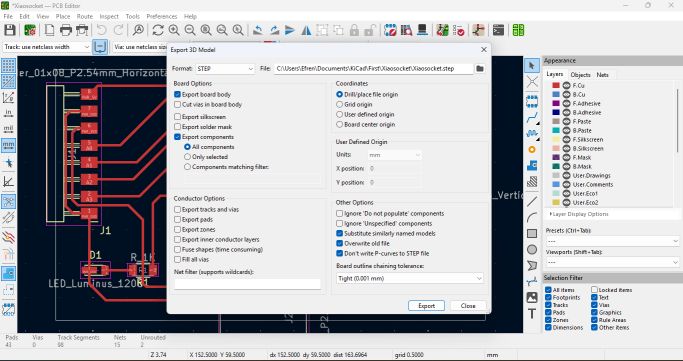
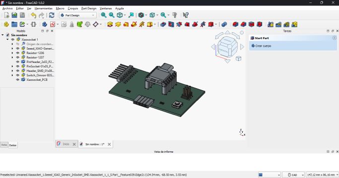
Finally, the design rule check (DRC) was successful, allowing me to generate the 3D image and BOM. I also exported the design in STEP format to work with it later in FreeCAD.
A few details: the DRC assumes that for the push button, both terminals must be connected. This is actually unnecessary since they are already connected internally, but the software will either show an error or prevent placing traces underneath the button. In my case, I managed to avoid routing underneath while avoiding errors.
We also implemented a pulldown resistor to eliminate noise on the RP2040 D7 input.
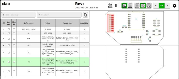
I generated a Bill of Materials (BOM) to list all components, footprints, and quantities required for the assembly process.
CONCLUSION
My experience with this assignment, as with all of them, has been very positive. However, in this case, since the topic was not entirely unfamiliar to me, I was able to compare and learn new techniques, discover equipment I had not used before, and deepen my understanding of electronics.
Of all the aspects, what I enjoyed the most were the EDA software tools, specifically KiCad, since my only previous experience with designing electronic boards was many years ago, drawing traces manually and using acids to etch them. This software allows you to design very easily and, most importantly, understand what you are doing.