Week 8
Electronics Production
Contents
Starting Point
In this case, although practically everything was new to me, I can say it felt somewhat familiar. While I had never built, repaired, or soldered a PCB before, I was fairly proficient with a soldering iron. Many years ago, I made or repaired my own audio cables, so I was used to soldering audio connectors (XLR, jack, mini-jack, RCA, etc.).
Obviously, the precision and finesse required when soldering a PCB is much greater than when soldering an audio connector, but it wasn't like facing the unknown when I had to do that part.
Group assignment
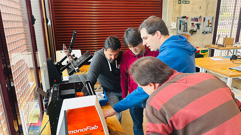
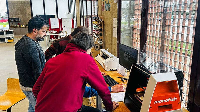
In this week’s group assignment we worked with the Roland MonoFab SRM-20, a relatively new machine in our FabLab. In fact, it is the latest machine acquired by the lab and it is still in the process of being set up and calibrated, so this activity also helped us become familiar with its operation and configuration.
During the exercise we learned about the main characteristics of the machine and how to operate it, as well as the complete workflow required to fabricate a PCB using this equipment.
We also reviewed the process of preparing the fabrication files, starting from the generation of the Gerber files to the creation of the milling toolpaths that are later used to machine the board.
Finally, we completed the workflow by milling the PCB and soldering the components, turning our electronic design into a fully functional board.
FabLab León 2026 Group Page ↗️
Characterize the design rules for your in-house PCB production process: document the settings for your machine.
In our FabLab we use the Roland MonoFab SRM-20 for in-house PCB production. As part of the group assignment, we carried out a series of tests to characterize the design rules and manufacturing parameters of our PCB production workflow.
Roland monoFab SRM-20 specifications, Safety and Workflow: Roland monoFab SRM-20
Virtually the entire workflow is repeated in the individual assignment section
For these tests we used the test patterns provided by FabAcademy:
- Traces: linetest.traces.png ↗️
- Cut / Interior: linetest.interior.png ↗️
These templates allow us to check the minimum trace resolution and the behavior of the cutting process, helping us define the manufacturing limits of the machine.
The complete file preparation and machining workflow for this machine can be found on the specific SRM-20 page in my documentation, or further below in the Individual Assignment section, where I explain the process step by step using my PCB as an example.
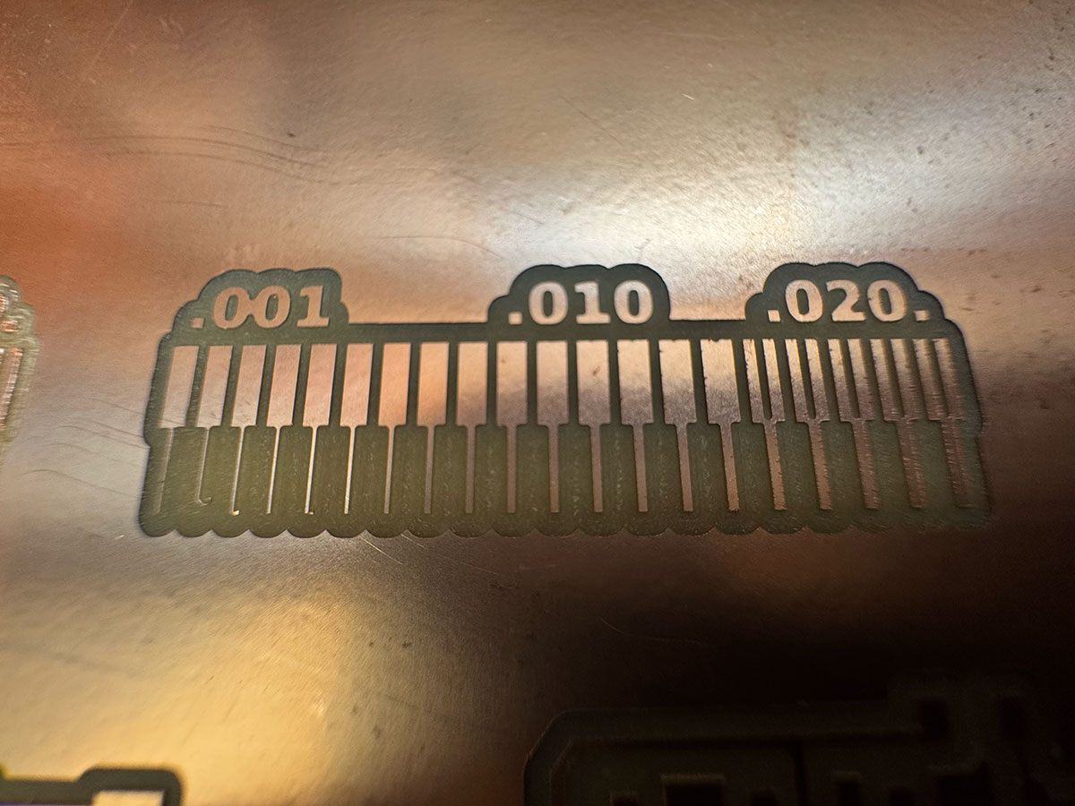
Once the files were prepared and processed on the machine, we obtained the characterization test result, which allowed us to evaluate the behavior of the different trace spacings and confirm the appropriate parameters for our in-house PCB production process.
This was the result obtained after processing the test patterns:
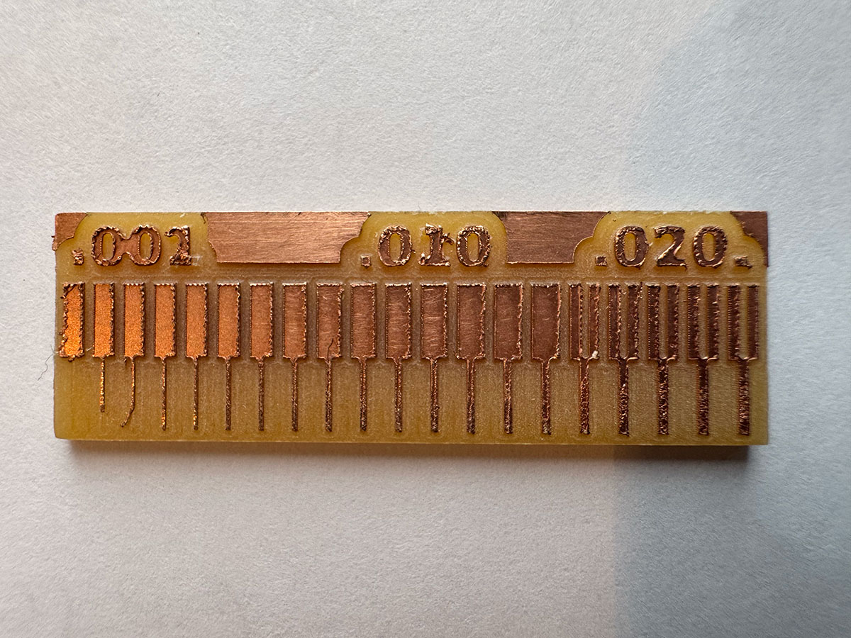
Note: The Roland MonoFab SRM-20 is still in the process of being set up and calibrated. Progress info.
Document the workflow for sending a PCB to a boardhouse
Sending the PCB to a boardhouse
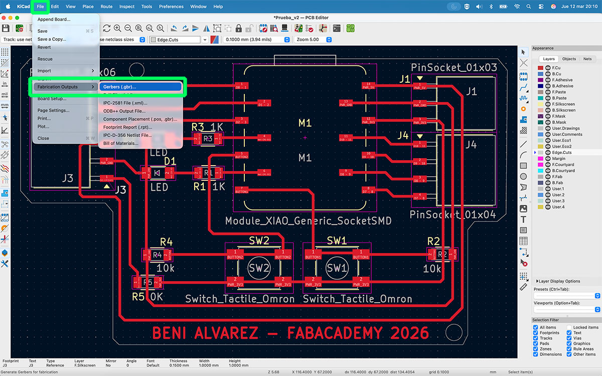
For this process I used the same PCB I had designed during the Electronics Design week. The goal here was to generate the manufacturing files needed to send the board to a PCB fabrication company.
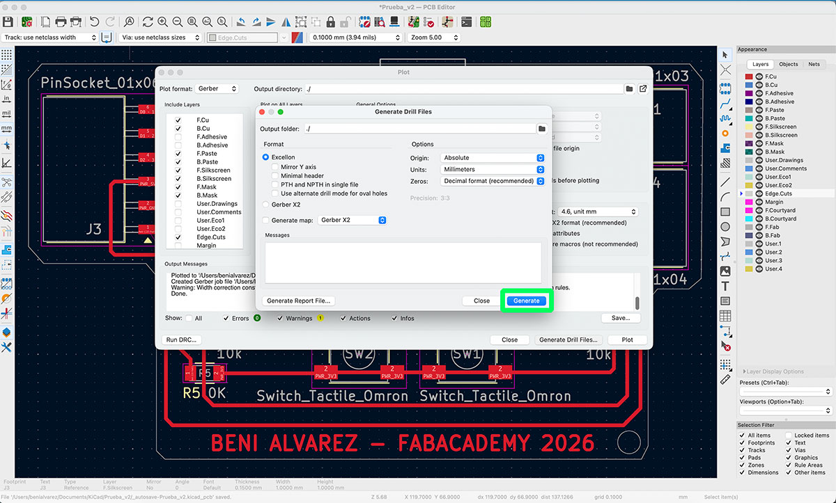
I started by opening my PCB project in KiCad and then going to File → Fabrication Outputs → Gerbers (.gbr).
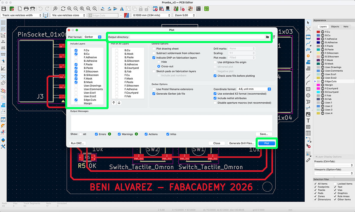
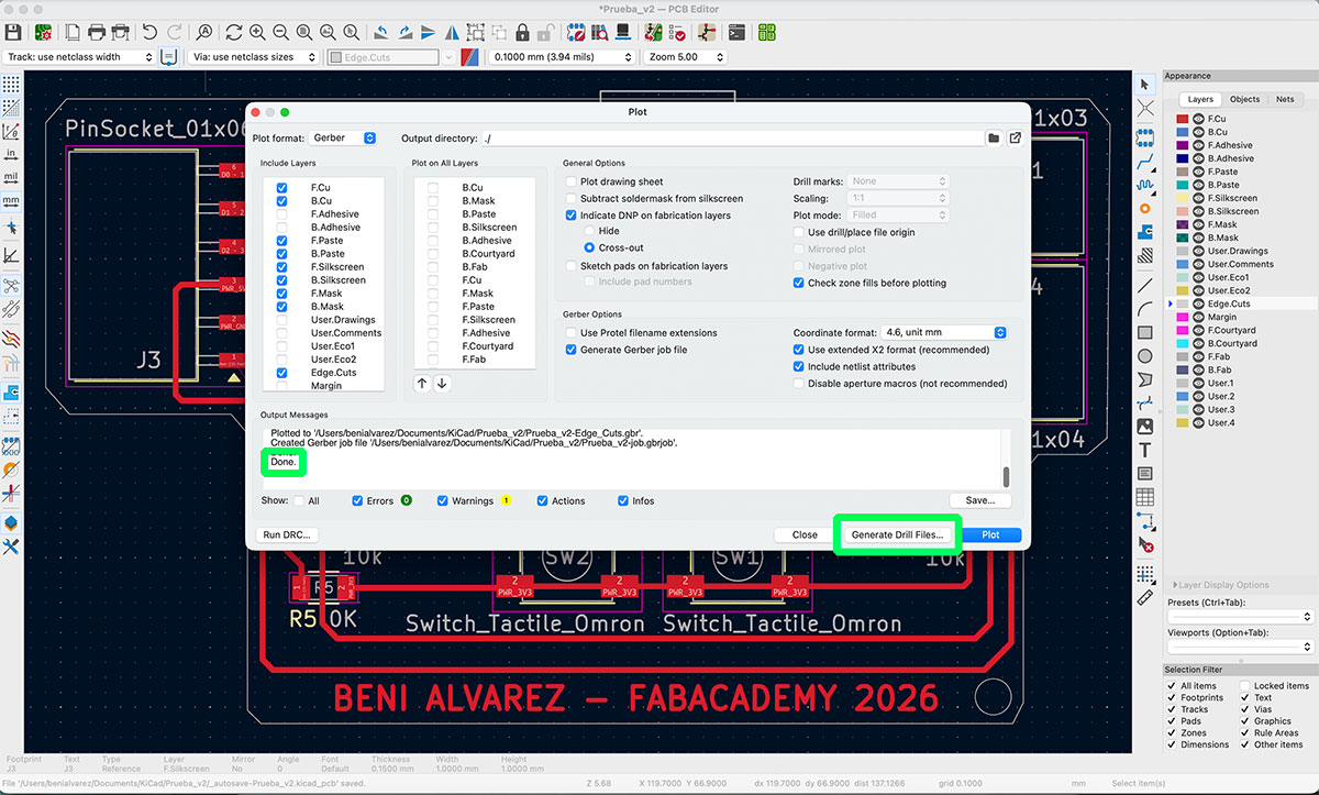
In the Gerber export window, I selected the destination folder where I wanted the files to be saved, chose the layers needed for fabrication, and then clicked “Plot” to generate the Gerber files. Once the message “Done” appeared, I continued with the drill files.
To generate them, I clicked on “Generate Drill Files…”. This opened a new dialog window, where I simply pressed “Generate” so KiCad could create the drill data as well.
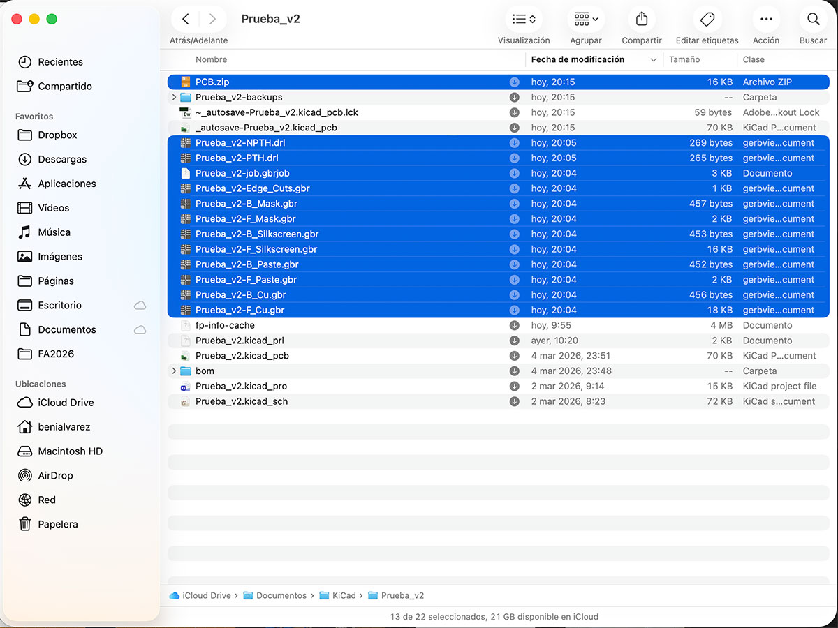
After that, I went to the output folder and checked that the process had generated a total of 12 files. These files include both the different board layers and the drill information required by the manufacturer.
To make the upload easier, I compressed all the generated files into a single .zip file. In my case, I named it “PCB.zip”.
This same .zip file will be used later both for the Group Assignment and for the Individual Assignment.
Simulating the PCB order to a boardhouse
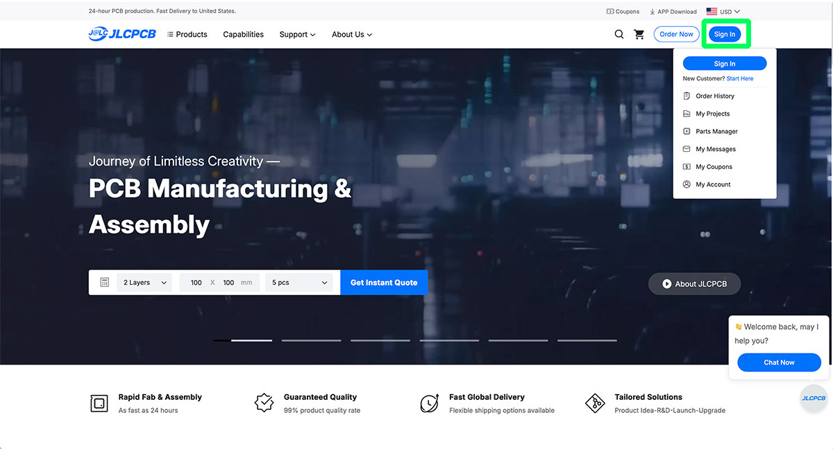
Once the fabrication files were generated, the next step was to simulate sending the board to a professional PCB manufacturing service. For this test I decided to use the online service provided by JLCPCB.
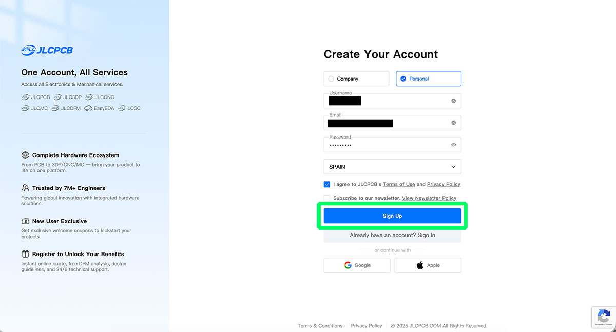
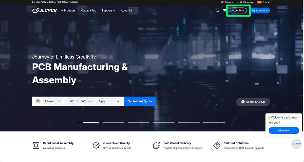
First, I accessed the website jlcpcb.com ↗️ and went to the “Sign In” option. If you already have an account you can simply log in, but in my case I created a new account and completed the registration process.
Once logged in, I selected the “Order now” option to start the PCB manufacturing process. At this stage the platform asks for the fabrication files, so I uploaded the .zip file previously generated in KiCad. The system only accepts .zip or .rar files with a maximum size of 100 MB, so the file prepared earlier fits perfectly within these requirements.
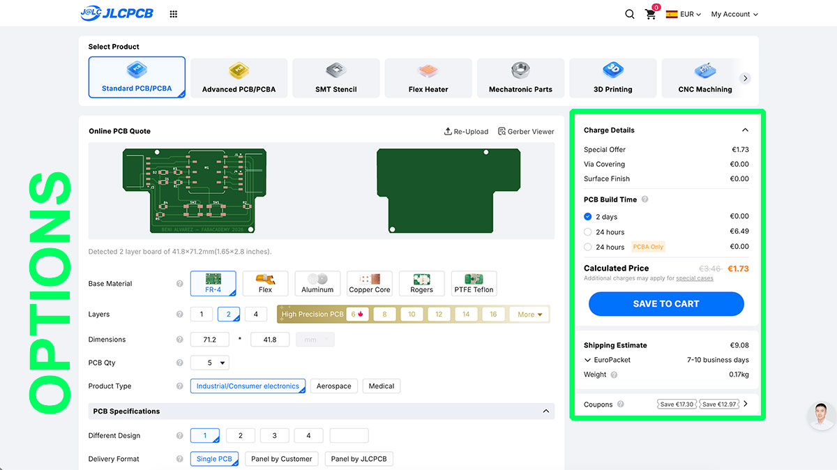
After uploading the file, the platform automatically generates a preview of the PCB. This allows checking that the design has been correctly interpreted before continuing with the order.
From this point, the website allows configuring many different parameters related to the PCB manufacturing process. These settings are organized into several sections.
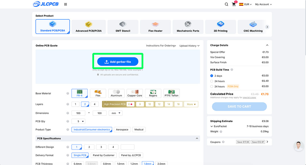
The first one is Online PCB Quote, where the main board parameters are defined, such as the base material, number of layers, board dimensions, PCB quantity, and product type.
Inside this section there are also the PCB Specifications, where additional characteristics can be configured, including the delivery format, PCB thickness, board color, silkscreen, material type, and surface finish.
More advanced settings are grouped under High-spec Options and Advanced Options. These include parameters such as outer copper weight, via covering, via plating method, minimum via size, board outline tolerance, electrical testing, and silkscreen technology, among many other possibilities.
The platform also offers additional services such as PCB Assembly, which allows ordering the automatic assembly of components, and the manufacturing of stencils for solder paste application.
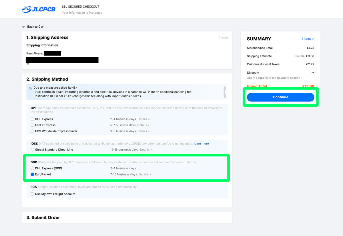
For this simulation I selected basic options and the minimum board quantity. With this configuration the system calculated a manufacturing cost of €1.73 for the 2-day production option, with no additional cost.
For shipping, I chose an economical delivery option to Spain with an estimated delivery time of 7–10 days, which cost €9.08. Faster shipping options were also available but at a considerably higher price.
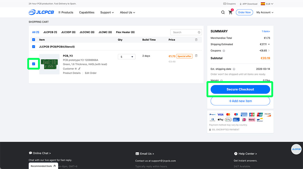
Once everything was configured, I added the order to the cart using the “Save to cart” option.
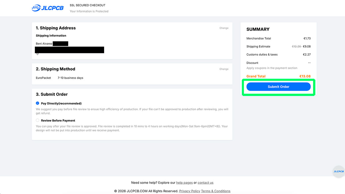
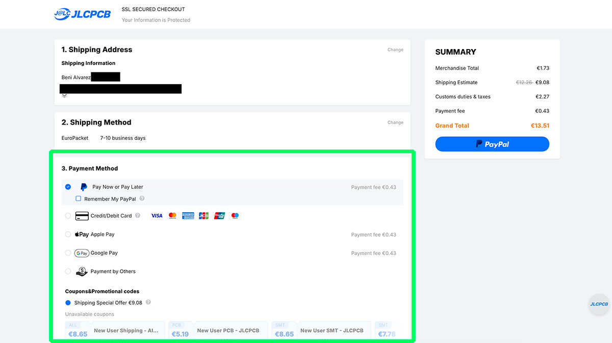
From the cart, the purchasing process continues by filling in the required information across several pages, including name, address, shipping details, and payment method.
Since my goal was only to simulate the process, I did not complete the purchase. I cancelled the order in the final step, during the payment method selection.
Document your work on the group work page and reflect what you learned on your individual page
I have reflected in the individual part of the assignment everything we learned in the group assignment, in this case, the complete flow from our PCB CAD design to seeing it finished and ready to work with.
Individual assignment
Make and test a microcontroller development board that you designed
Generating images from the Gerbers
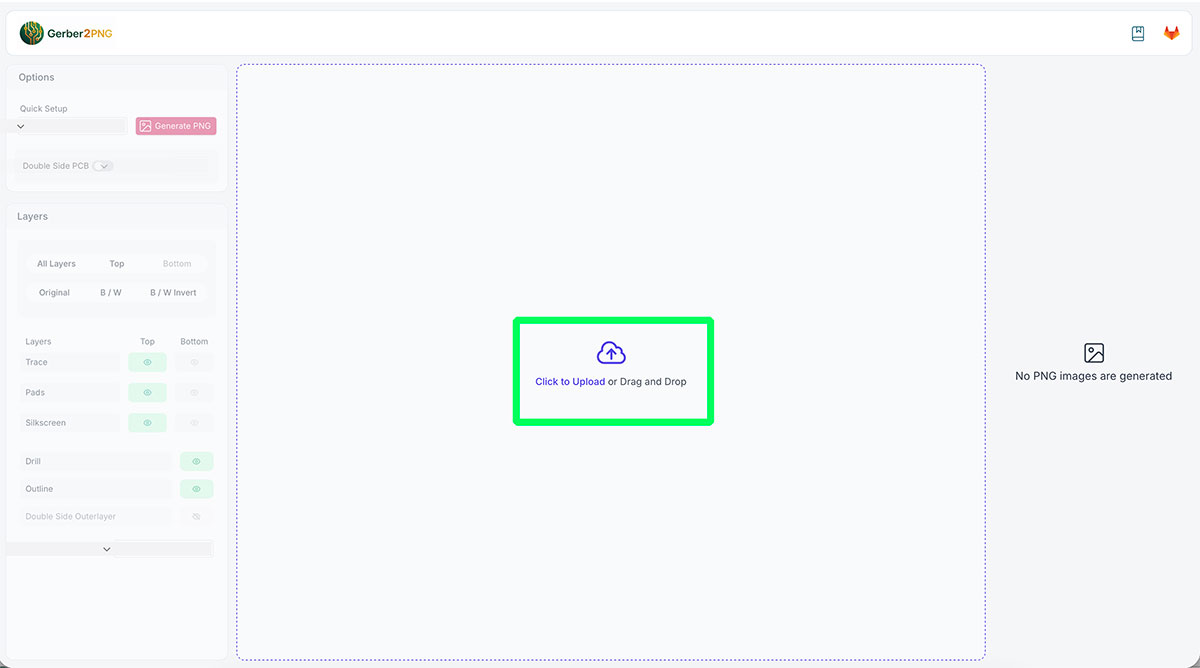
Once the Gerber files were generated, the next step was to convert them into PNG images that can later be used to generate the PCB milling toolpaths.
For this task I used the tool Gerber2PNG, developed by FabLab Kerala, available at: https://gerber2png.fablabkerala.in ↗️
This tool allows uploading directly the same .zip file previously generated in KiCad, which contains both the Gerber files and the drill files.
As soon as the compressed file is uploaded, the platform automatically shows a preview of the PCB. This makes it easy to quickly verify that the design has been correctly loaded.
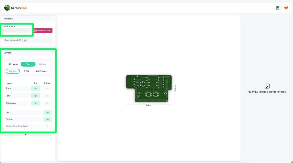
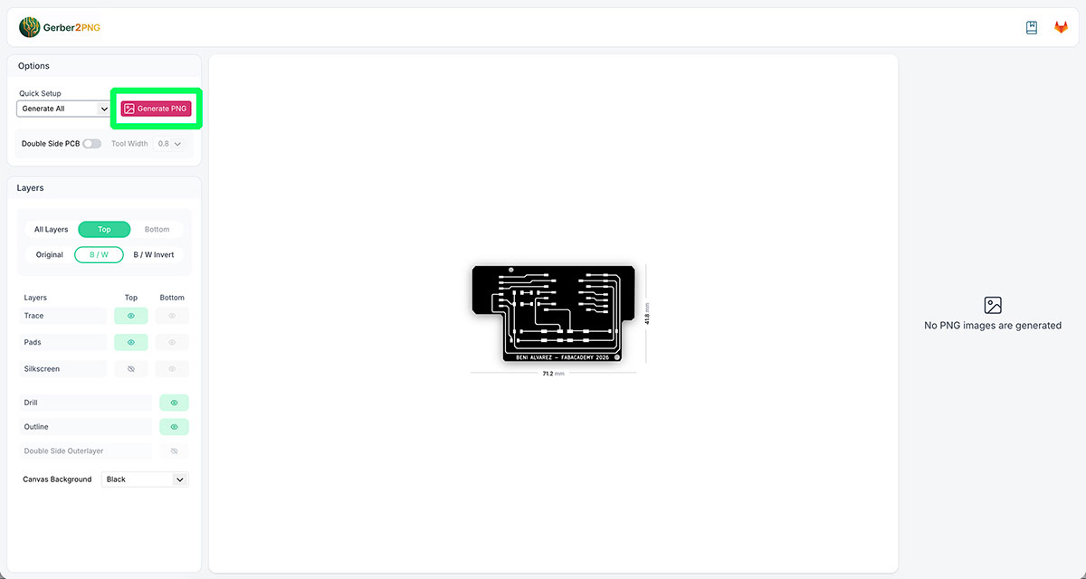
Next, I configured the generation options. First, I selected the option “Generate all” so the system would create all the required files. In the Layers section, I enabled the “B/W” layer and disabled “Silkscreen”, since in this case we are not milling the component labels on the board.
I also checked that in the “Quick Setup” section the option “Generate all” was still selected, as this configuration may change automatically when modifying other parameters.
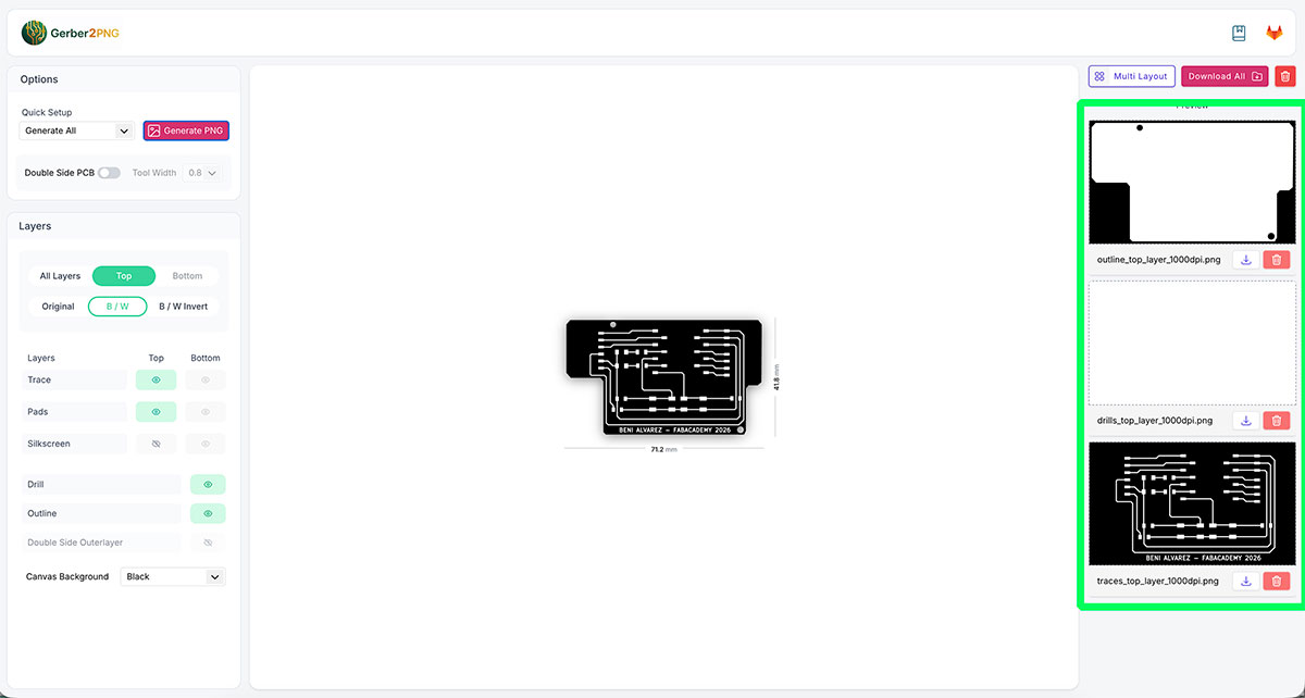
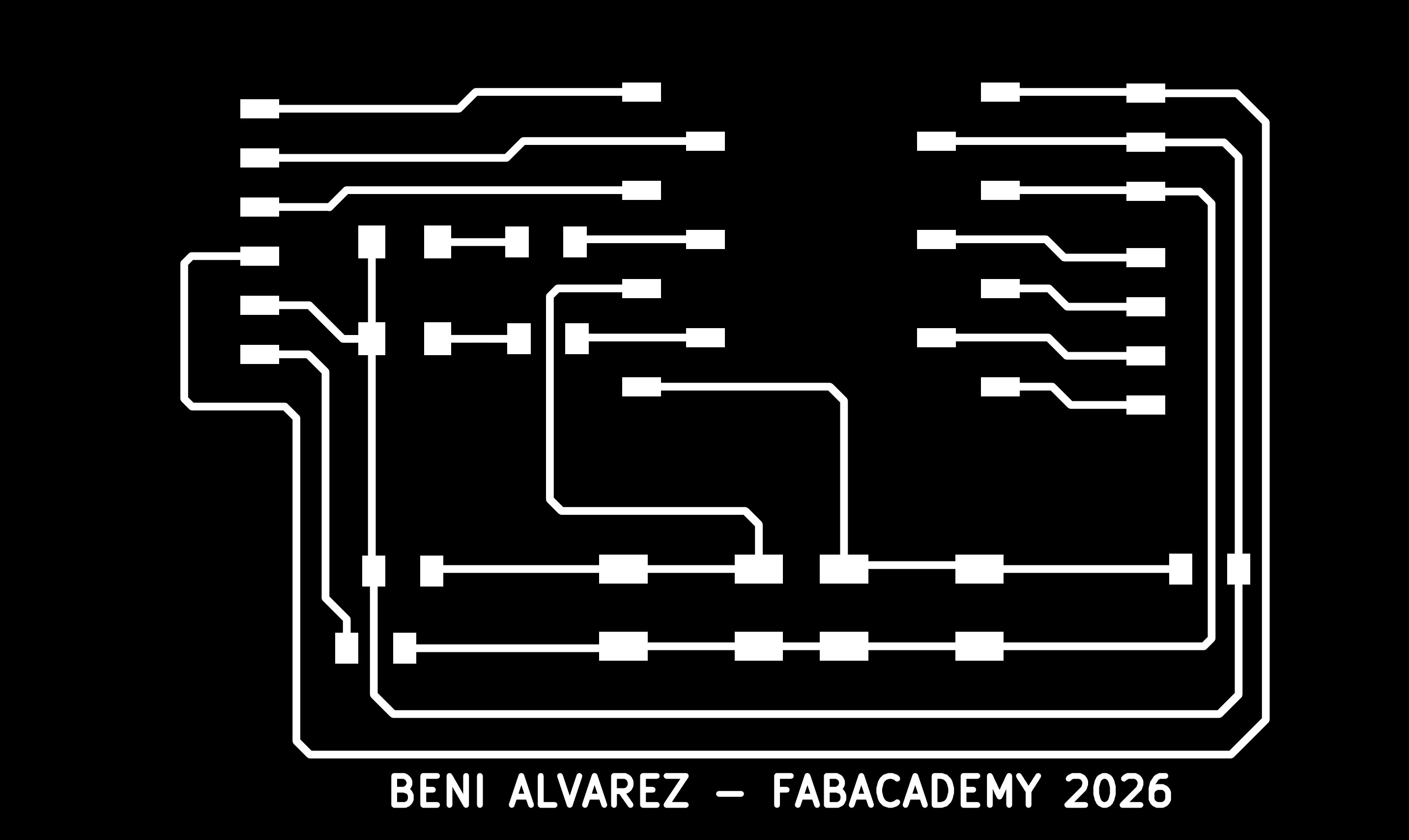
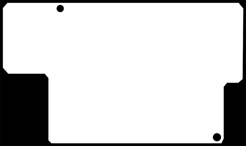
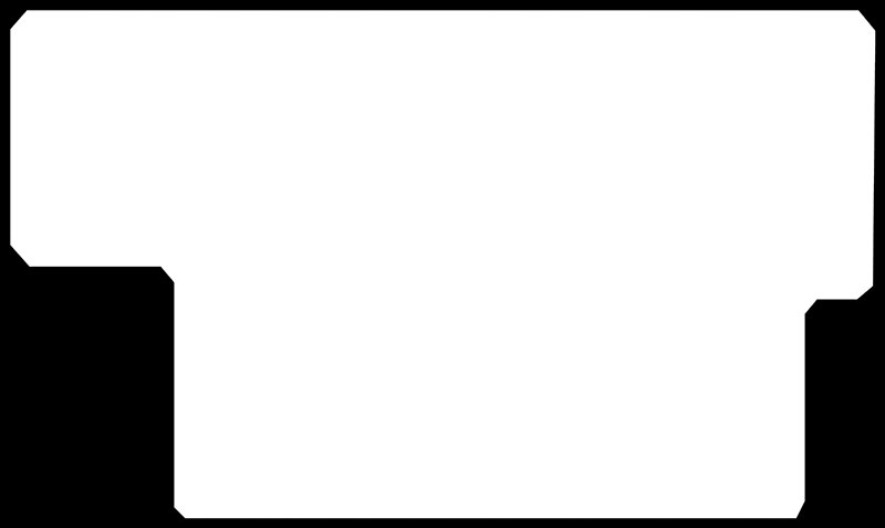
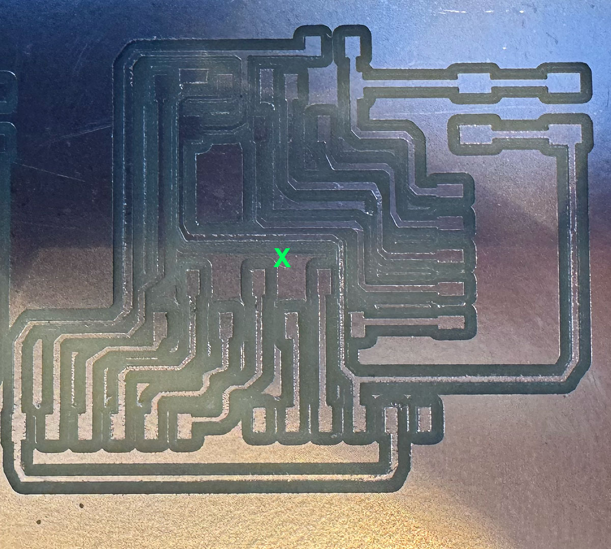
After configuring everything, I clicked “Generate PNG”. A few seconds later, the right column of the page displayed the three generated PNG files, corresponding to the outline, drills, and traces of the board. These are the files that will be downloaded and later used in the milling process.
In these images the color code is important: the white areas represent the copper that will remain on the board, while the black areas correspond to the material that the milling tool will remove.
Later, when configuring the machining toolpaths, the number of tool passes will determine how much material is removed around the traces to properly isolate the connections.
Mods Project
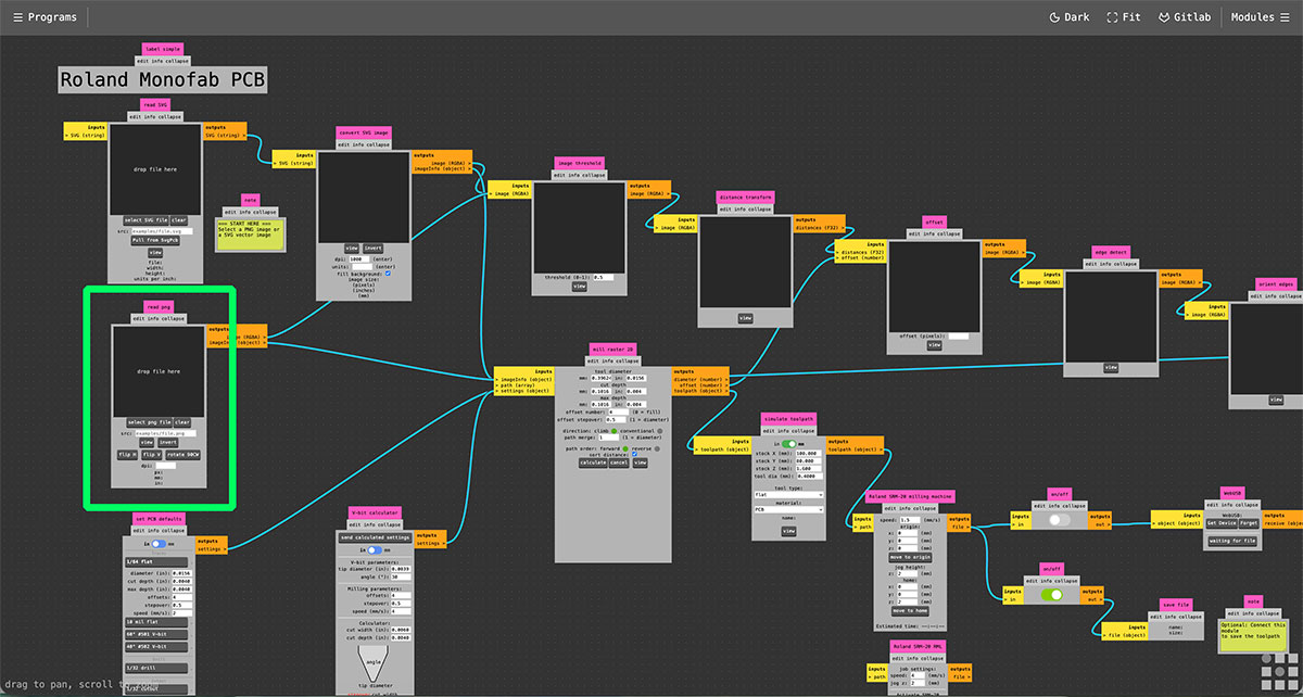
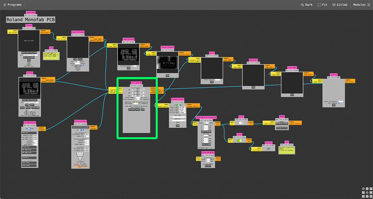
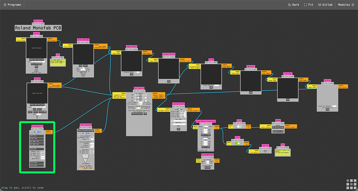
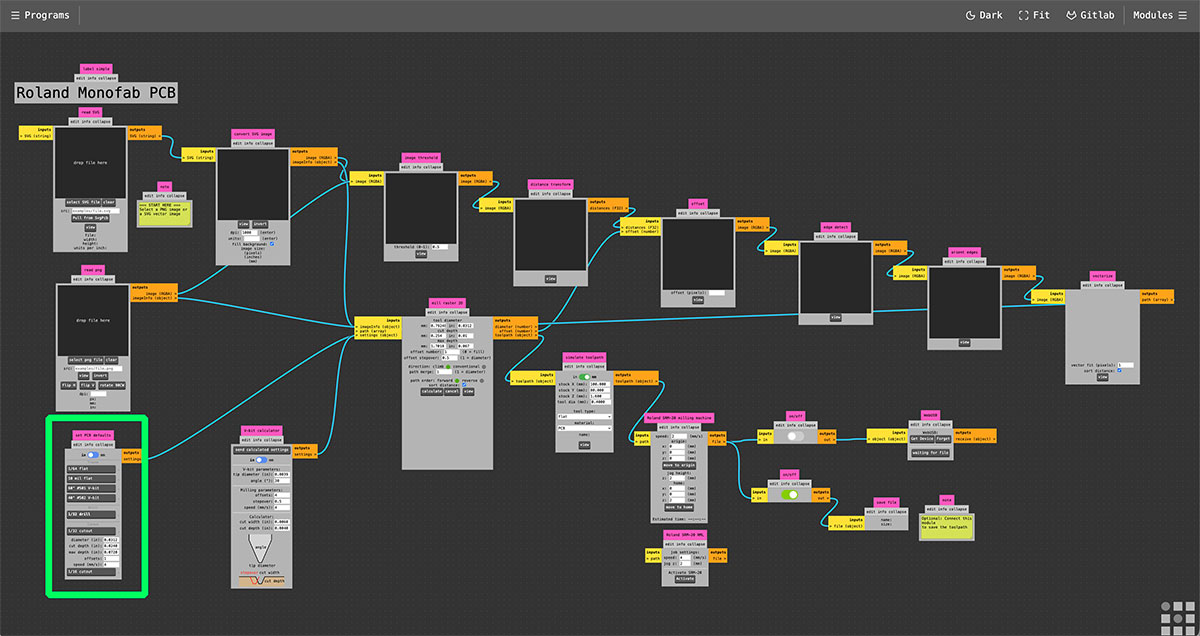
Once the PNG images were downloaded, the next step was to generate the toolpath files that the milling machine will use to machine the PCB.
For this task I used the web application Mods Project,
available at: https://modsproject.org/ ↗️
This tool is designed to work with digital fabrication machines and it is
optimized to run in Google Chrome.
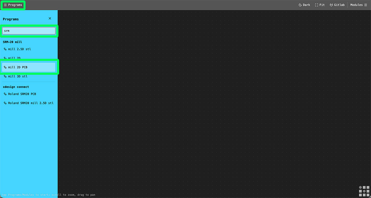
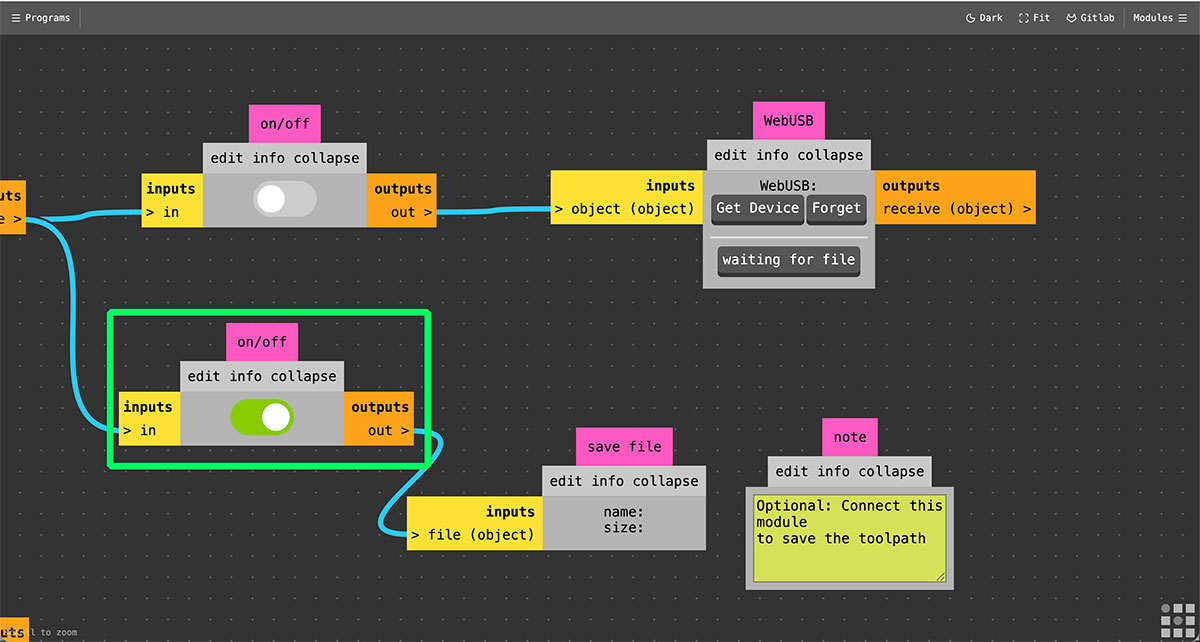
After entering the website, I opened the “Programs” menu. In the search field I typed “srm” so the platform could list the available workflows related to the Roland milling machines. In this case I selected “mill 2D PCB”, which loads the workflow specifically designed for milling PCBs with this machine.
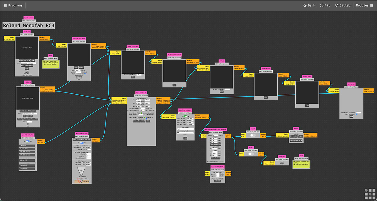
At the end of the workflow there are two output modules. One allows sending the files directly to the milling machine using WebUSB, while the other allows saving the generated files. In this case I chose to generate and save the files, since I will later load them into the machine using the dedicated software VPanel. To do this, I went to the end of the workflow and activated the “Save file” option.
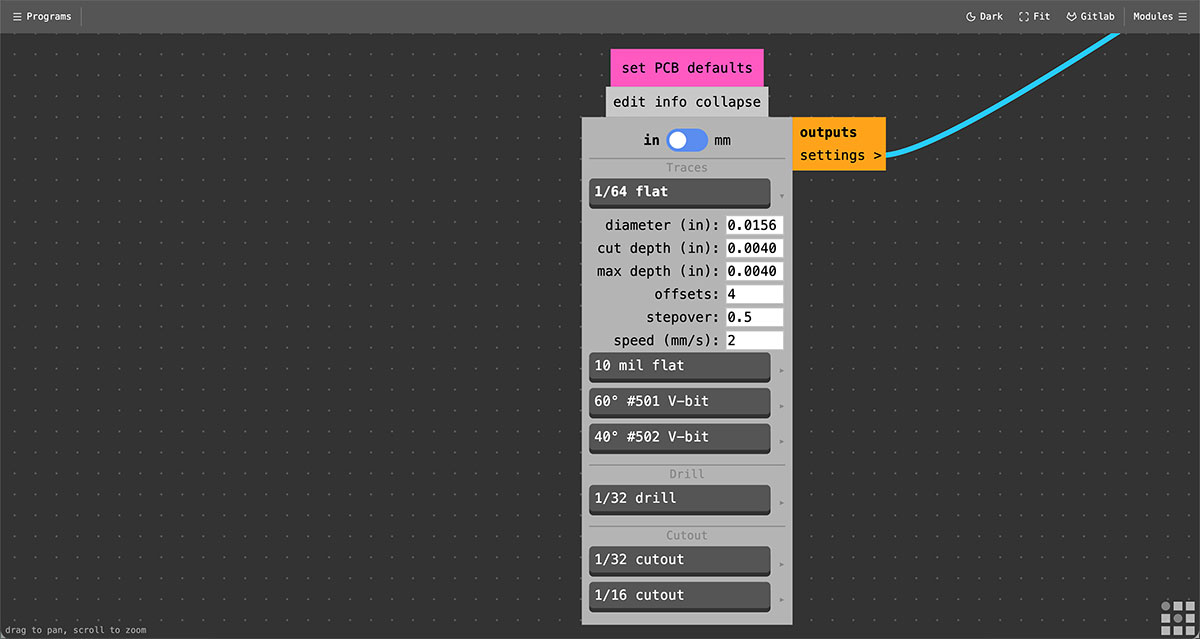
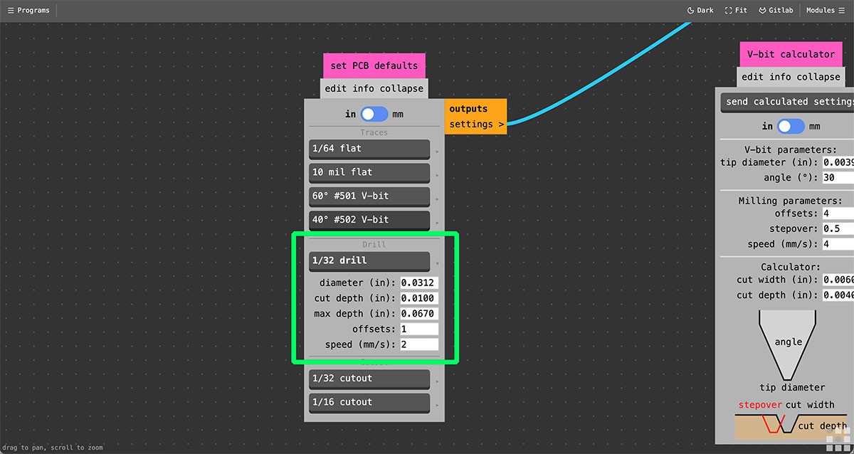
Then I returned to the first part of the workflow to configure the machining parameters. In the lower section of the corresponding module it is possible to define the parameters for the “Traces”, depending on the type of end mill that will be used.
In this case I selected “1/64 flat” by expanding the dropdown menu on the right side. Once selected, the parameters associated with that tool appear automatically. I kept all the default values except for the speed, which I set to 2 mm/s. After changing the value it is important to click the “1/64 flat” button so the configuration is properly applied.
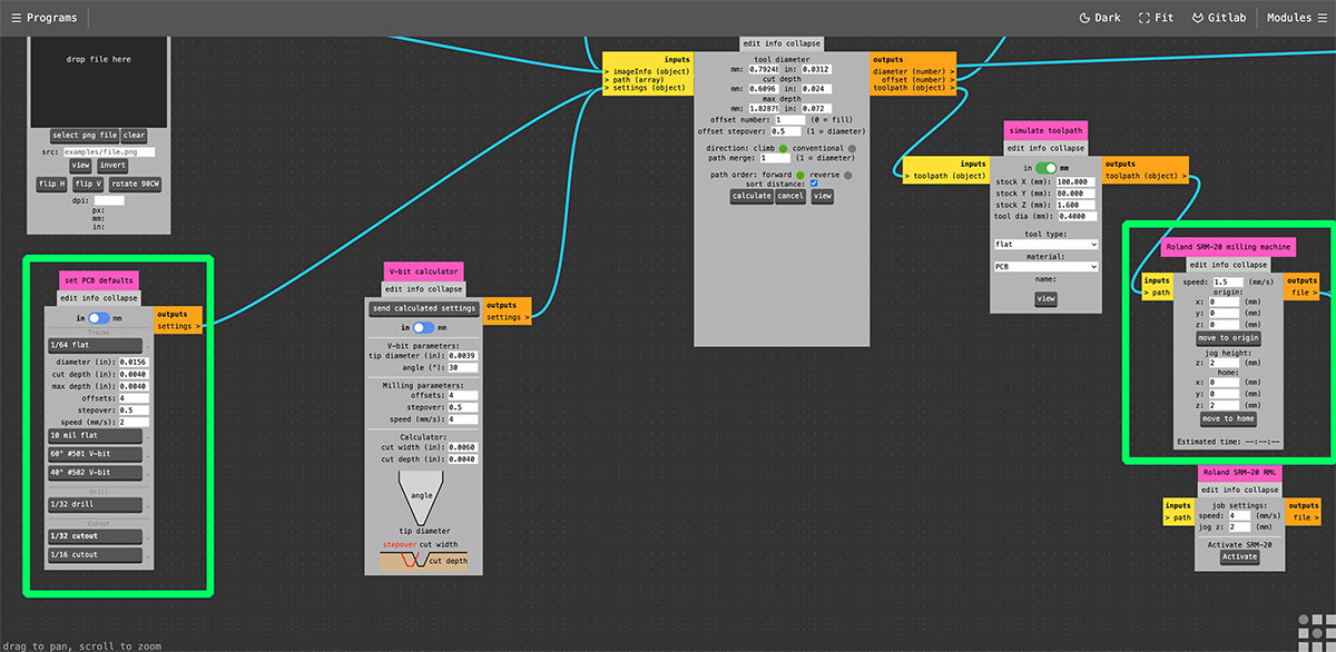
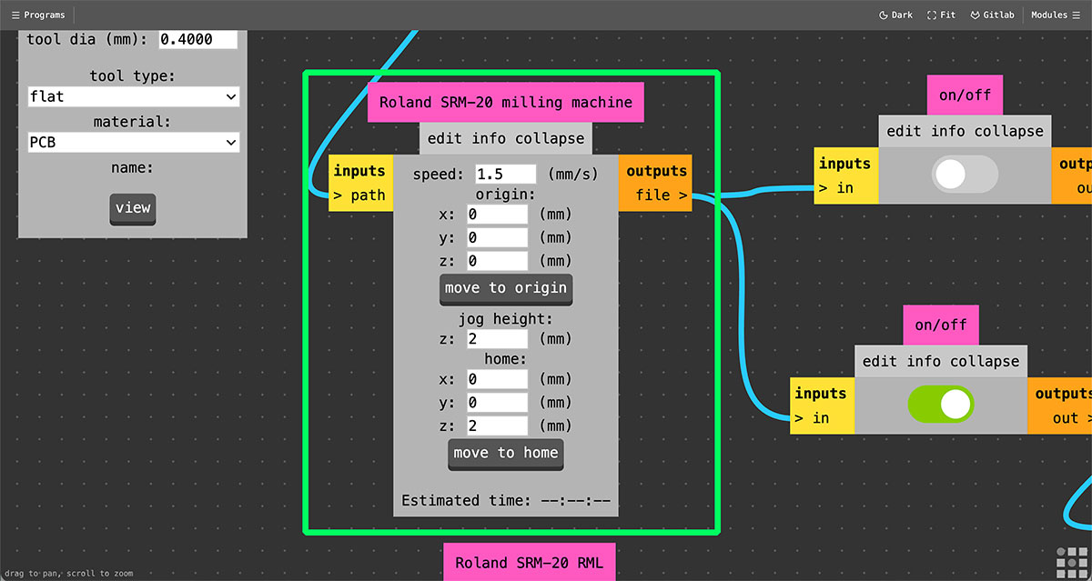
It is also necessary to adjust the speed in the “Roland SR-20 milling machine” module, which appears later in the workflow. In this module I configured the toolpath speed to 1.5 mm/s.
In the same module the machine origin and home positions are also defined. In my case I used the following configuration:
Origin: X:0, Y:0, Z:0 mm
Jog height: 2 mm
Home: X:0, Y:0, Z:2 mm
Setting the Z axis to 2 mm for the Home position ensures that the milling tool starts slightly above the surface, preventing the end mill from starting in direct contact with the PCB.
Generating the traces toolpath
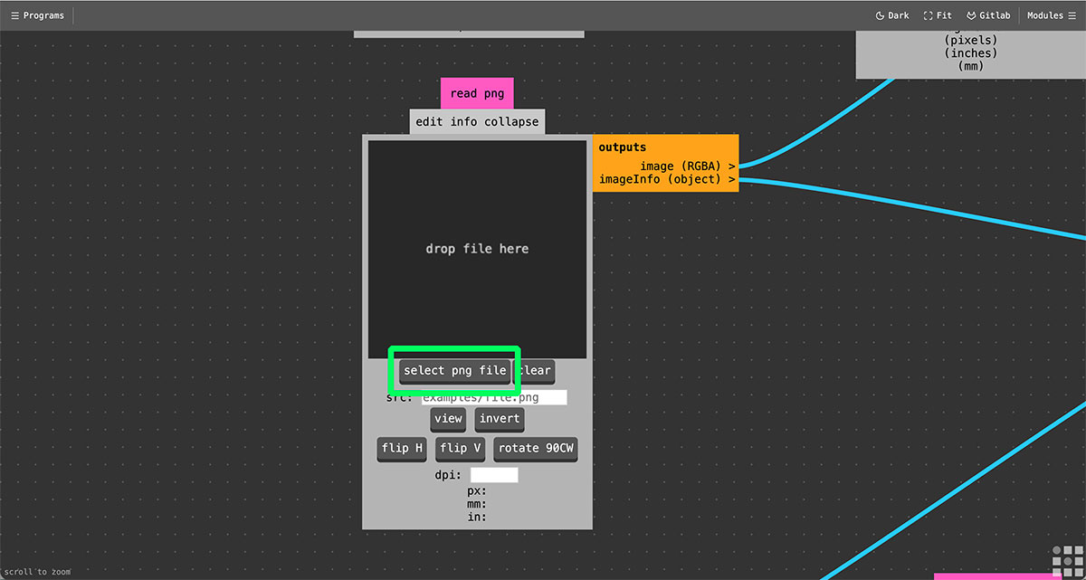
Once the parameters were configured in Mods, the next step was to load the previously generated images in order to create the milling toolpaths. In this case I started with the traces file.
At the beginning of the Mods workflow there are two image input modules: PNG and JPG. I loaded the file in the corresponding module, and the workflow automatically updated to display the PCB image in the following modules of the process.
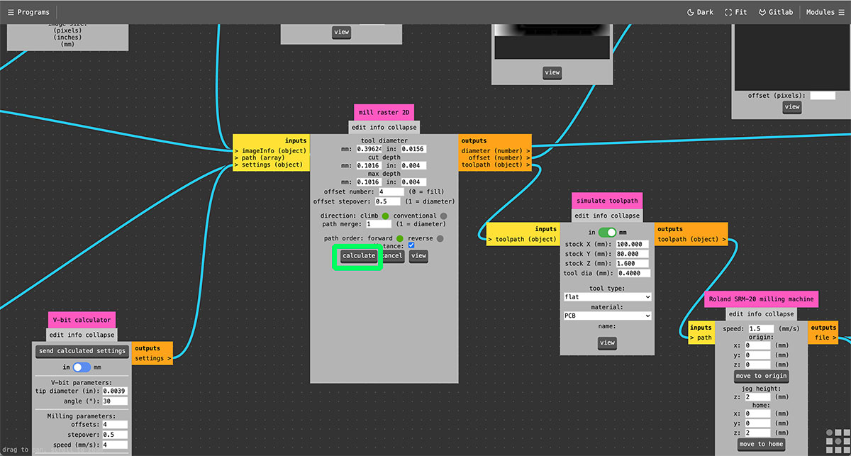
In the central part of the workflow we find the “mill raster 2D” module, which is responsible for calculating the milling paths from the loaded image.
To generate the toolpath I clicked the “Calculate” button. After doing this, the system processed the image and generated several intermediate visualizations in the boxes above, such as “offset”, “edge detect”, and “origin edges”. These views help verify how the design is being interpreted before creating the final file.
At the same time, Mods generates the machine control file in .rml format. This file is automatically created using the same name as the uploaded image. In my case the generated file was:
traces_top_layer_1000dpi.png.rml
Once the file is generated, it automatically opens in a new browser tab or window, showing a preview or simulation of the milling path that will be followed by the tool on the PCB.
It is important to note that the first time this process is executed, the browser may block the new window. In that case, it is necessary to allow pop-ups for the Mods website and repeat the process.
After generating the toolpath for the traces, the next step was to repeat the same process with the other two images previously generated: drills and outline.
In both cases I used a 1/32” end mill, which is suitable for drilling the holes and cutting the external contour of the PCB. In the corresponding module I selected “1/32 flat”, keeping all the default parameters except for the speed, which I set to 2 mm/s.
As done previously, it is also necessary to configure the toolpath speed in the “Roland SR-20 milling machine” module. In this case I also set the speed to 2 mm/s.
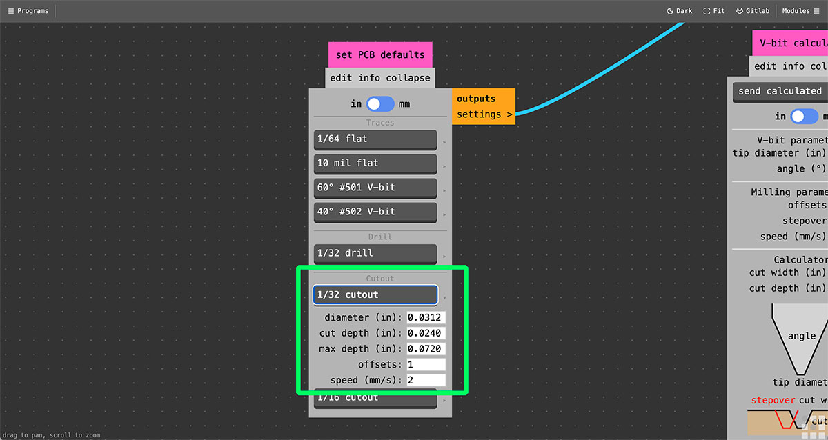
In the “Set PCB defaults” module I configured the specific parameters for each operation:
1/32” drills for generating the holes.
1/32” cutout for the external PCB cut.
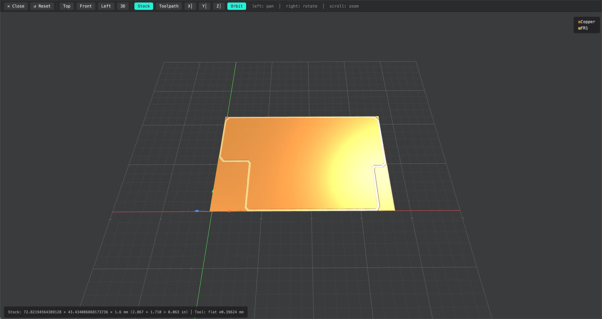
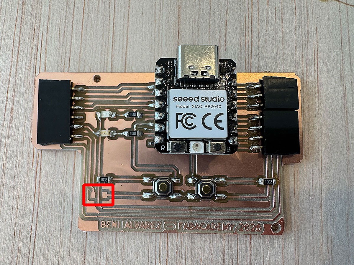
During this step I noticed that the outline image also contained the drill holes. To avoid the milling machine interpreting both operations in the same file, I decided to separate them into two different images.
To do this, I edited the image using GIMP. I created one file containing only the PCB outline (removing the drill circles), and another file containing only the drills.
This way I can generate independent toolpaths for each operation, which allows better control of the machining order and ensures that the appropriate tool is used for each process.


Once the files were prepared and the corresponding tools configured, I repeated the same procedure to generate the drill toolpaths.
To do this, I loaded the image corresponding to the holes and configured the tool parameters and machining type in the “Set PCB defaults” module, selecting the appropriate end mill and the drill toolpath option.
I then repeated the same process to generate the outline cut toolpath. Again, I loaded the image corresponding to the PCB contour and configured the parameters in the “Set PCB defaults” module, selecting the tool and the appropriate cutout toolpath.
SRM-20 Milling Parameters
| Tool | Diameter | Feed rate |
|---|---|---|
| 1/32” End Mill | 0.8 mm | 2 mm/s |
| 1/64” End Mill | 0.4 mm | 1.5 mm/s |
| Micro End Mill | 0.3 mm | 1 mm/s |
SRM-20 Machine parameter
| Machine parameter | Axis | Value |
|---|---|---|
| Origin | X | 0 mm |
| Y | 0 mm | |
| Z | 0 mm | |
| Jog height | Z | 2 mm |
| Home | X | 0 mm |
| Y | 0 mm | |
| Z | 2 mm |
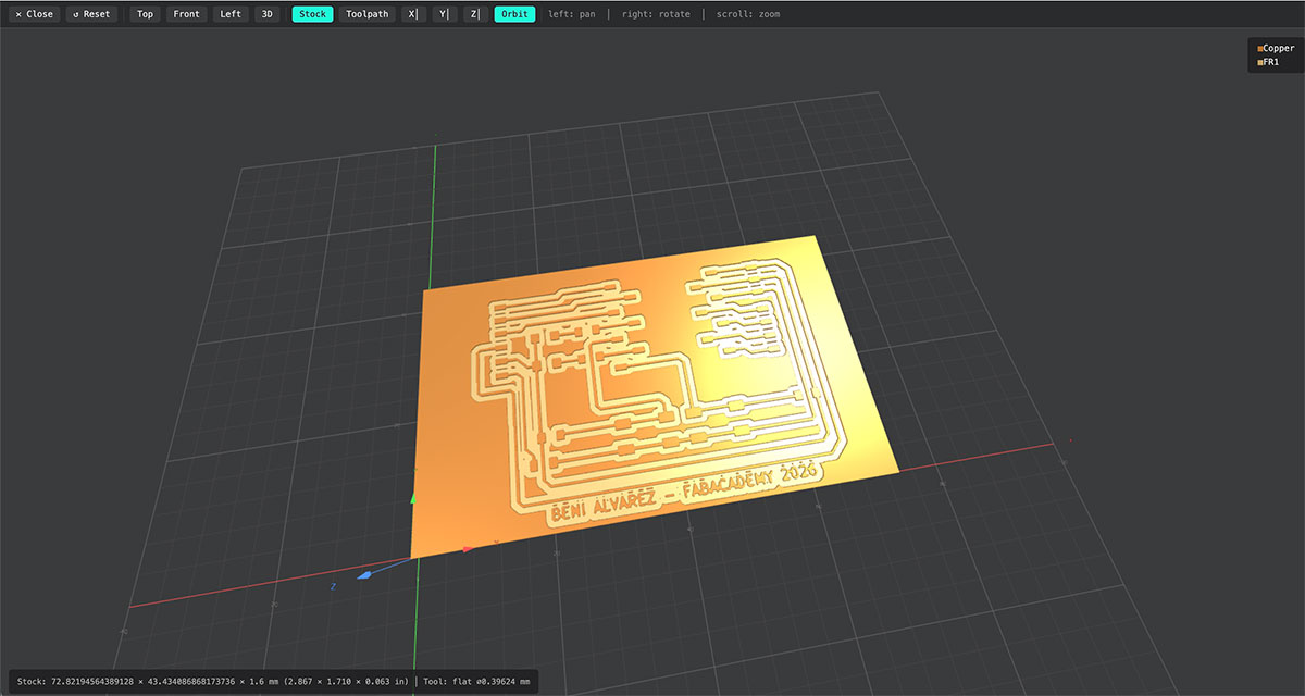
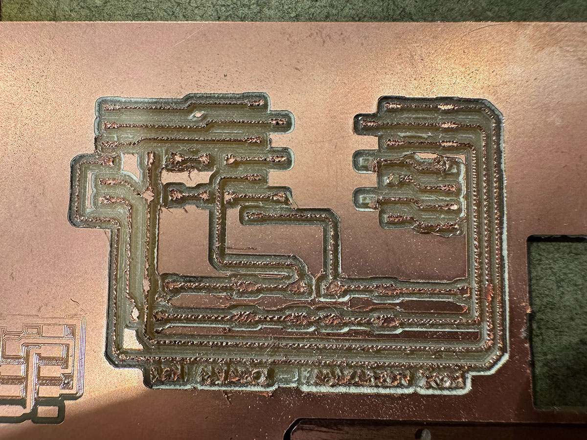
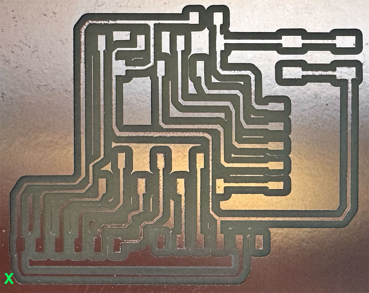
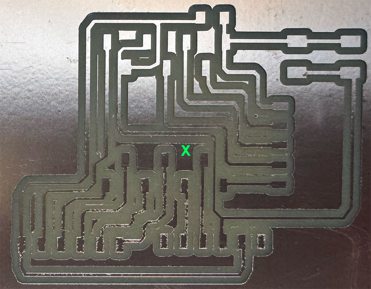
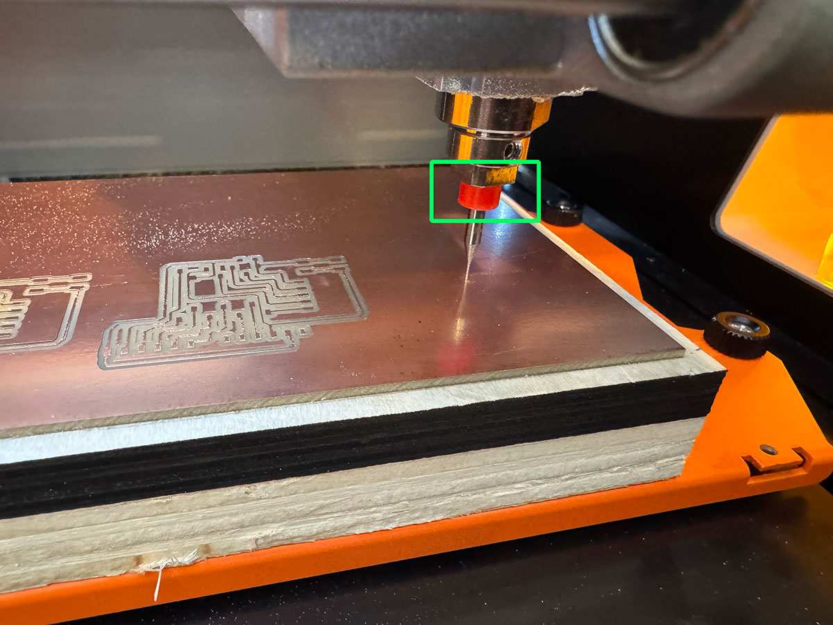
Milling the PCB on the Roland SRM-20
Once the .rml files were generated with Mods, the next step was to mill the PCB using the Roland SRM-20. This process involves both the physical preparation of the machine and the configuration of the job using the Roland VPanel software.
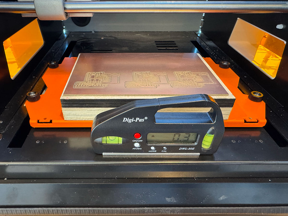
Machine physical preparation
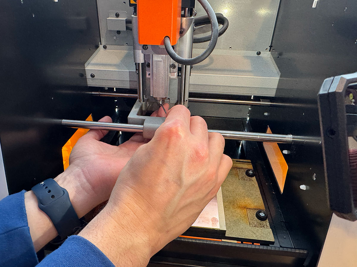
The first step is preparing the working surface. I fixed the PCB to the machine bed using double-sided tape, placing it on top of the sacrificial layer to ensure that the board remained firmly attached during the milling process.
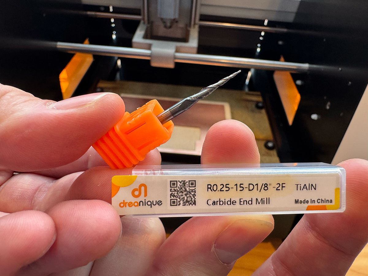
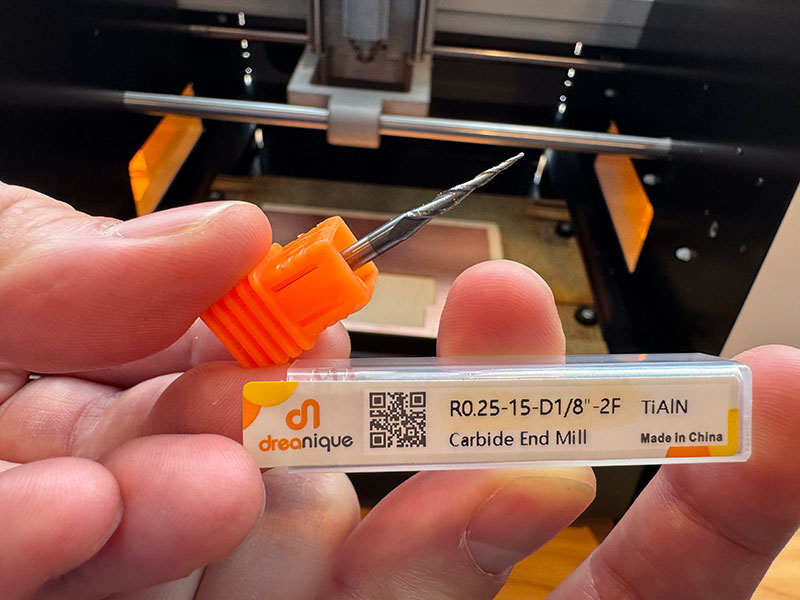
Next, I installed the 0.4 mm (1/64”) end mill, which is used for milling the PCB traces. The tool was inserted into the collet and secured by tightening the fixing screw. It is important that only one person manipulates the tool during this step to avoid unexpected movements or potential accidents.
Setting the origin in VPanel
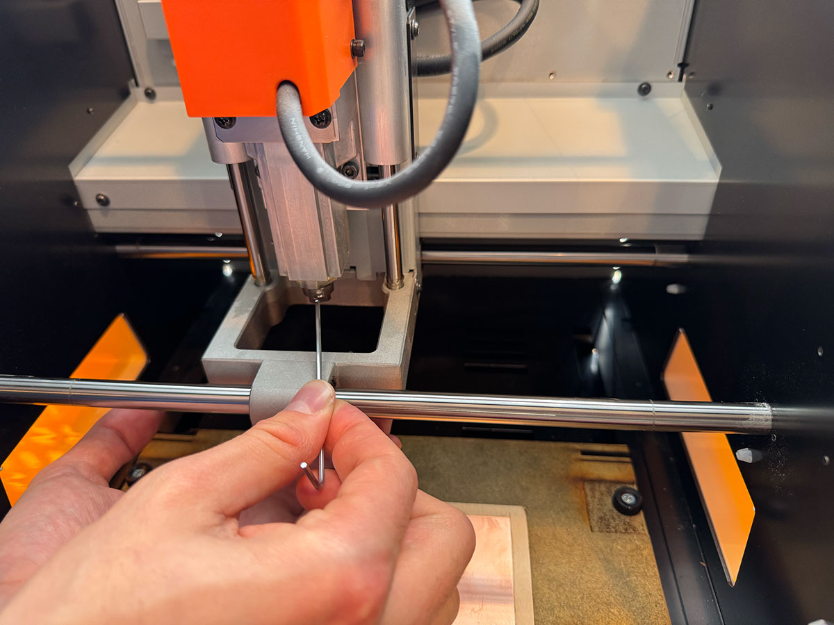
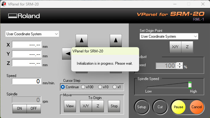
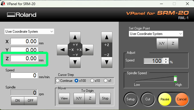
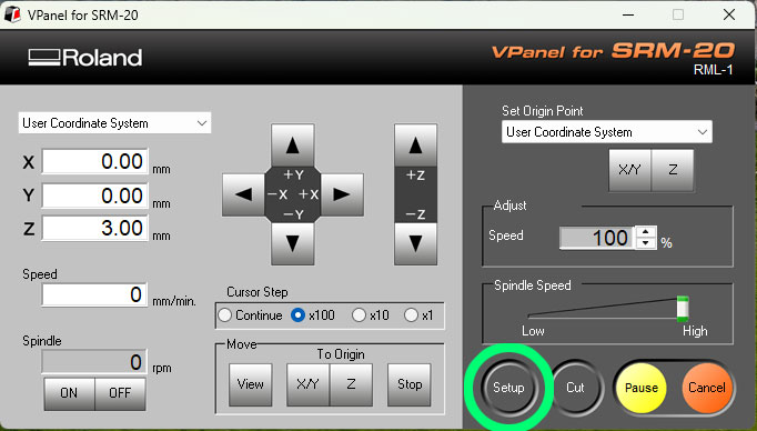
With the machine prepared, the next step is defining the milling origin using the Roland VPanel software.
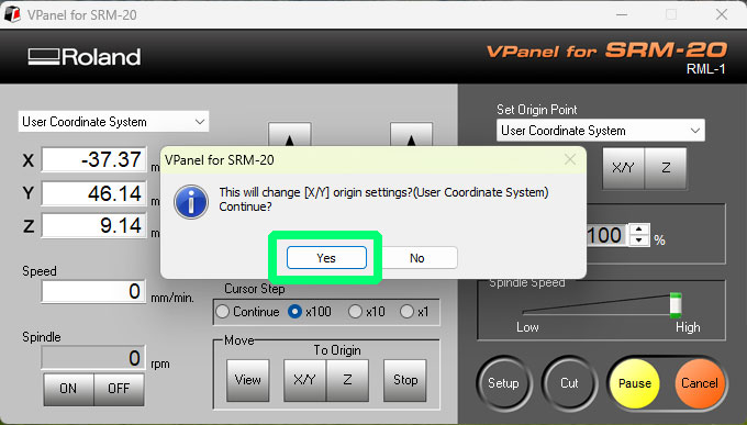
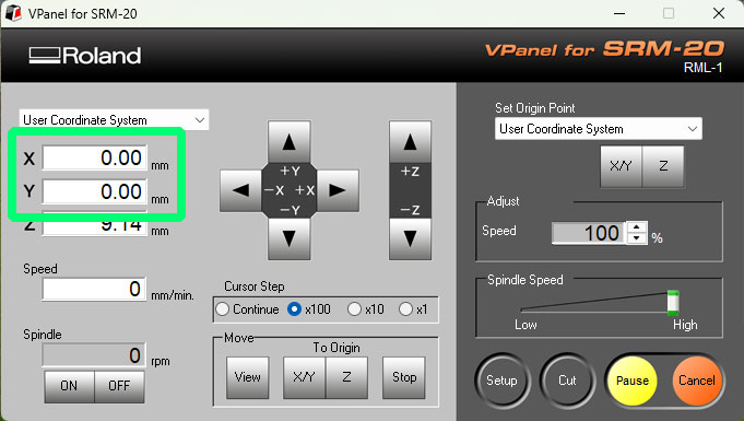
First, I adjusted the X and Y origin. Using the movement controls in VPanel, I positioned the tool over the desired point of the PCB and clicked “Set Origin Point – XY” to store that location.
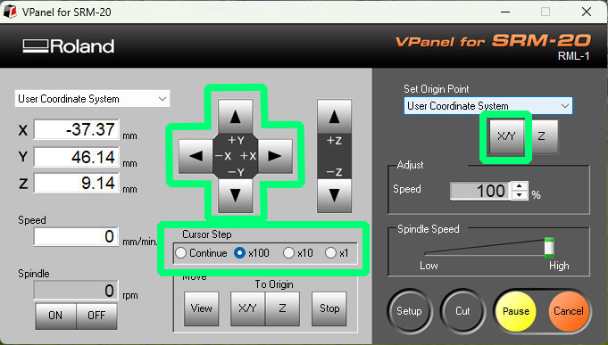
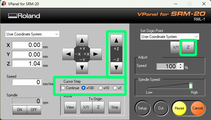
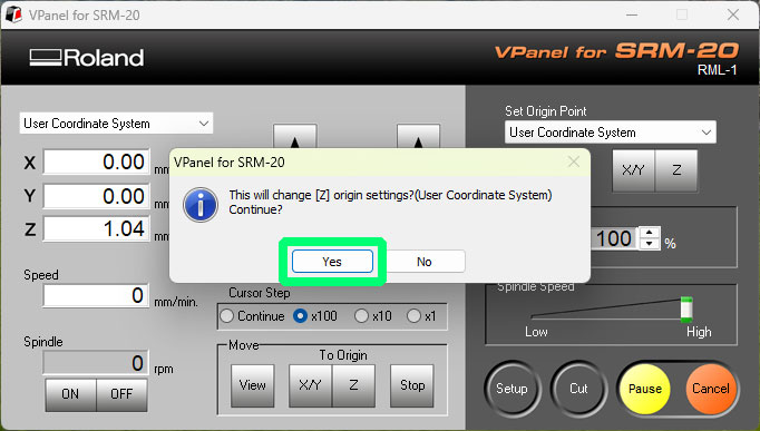
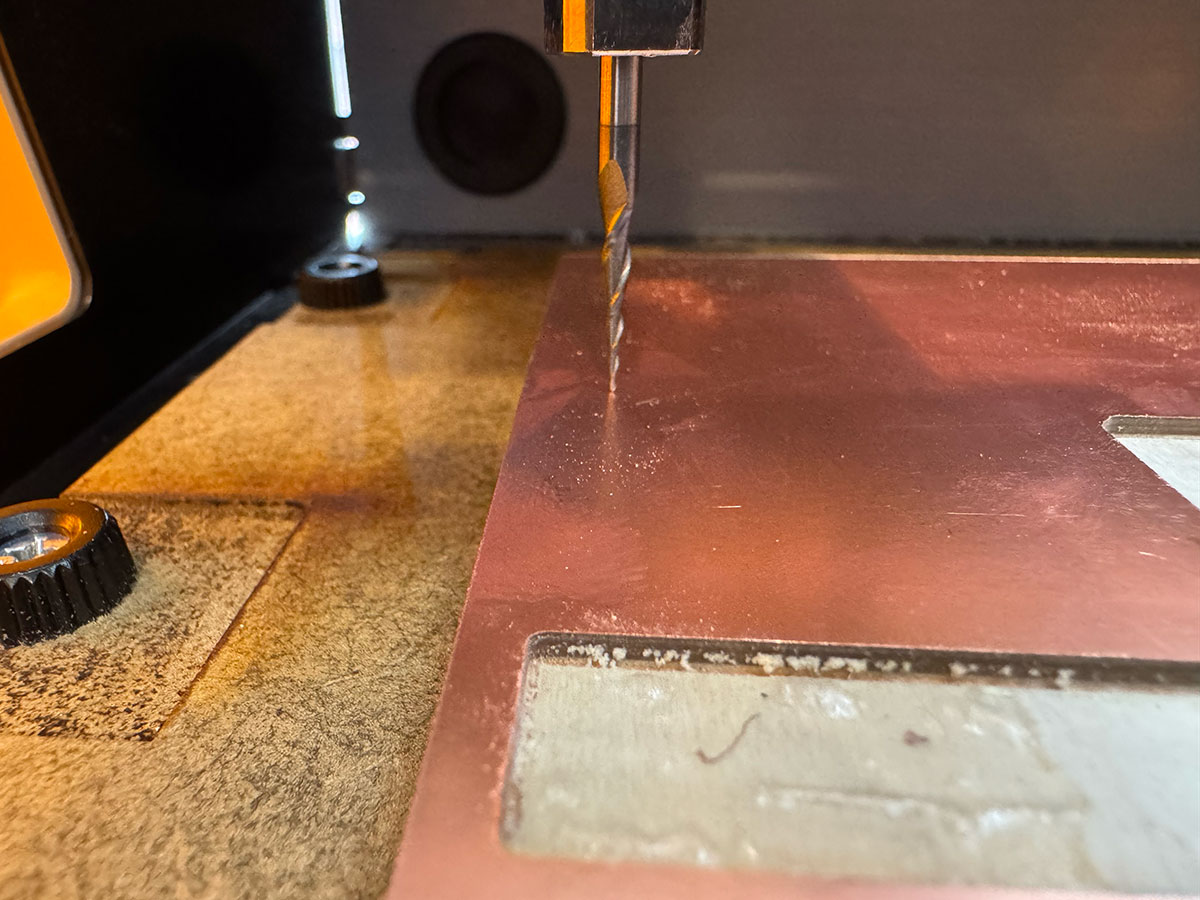
Then I adjusted the Z origin following the usual procedure:
1. Lower the Z axis until the tool is as close as possible to the PCB
surface using the movement controls.
2. Loosen the tool screw slightly and allow the end mill to
gently rest on the PCB surface.
3. Tighten the screw again to fix the tool position and press
“Set Origin Point Z”.
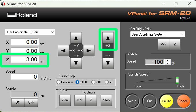
4. Raise the Z axis about 3 mm (using
Cursor Step x100) before starting the job.
Milling process
Once the origins were configured, the next step was sending the milling file to the machine.
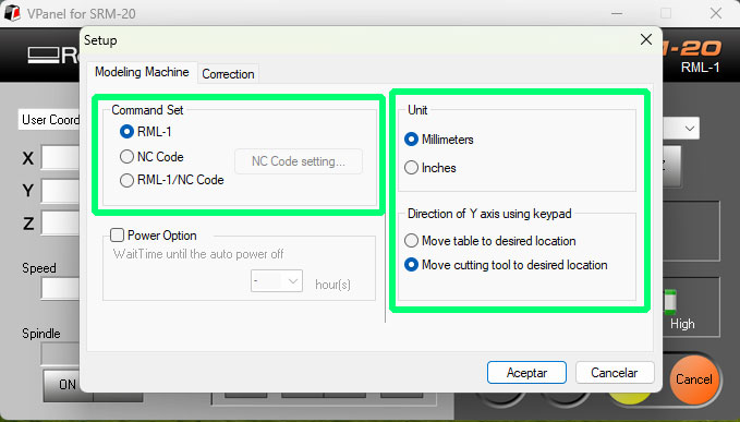
First, I opened the Setup menu in VPanel and verified that the options RML-1 → Millimeters and Move cutting tool were enabled. After confirming the configuration, I proceeded with the job setup.
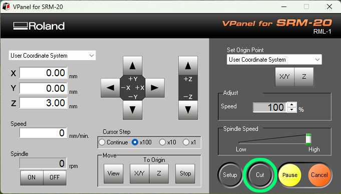
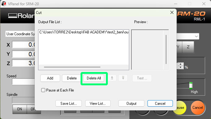
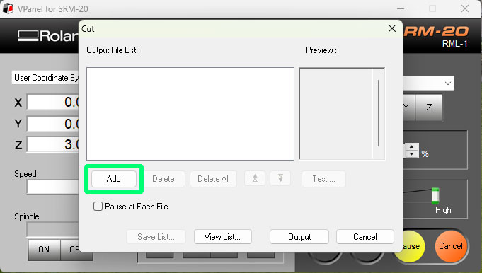
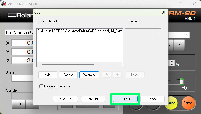
I then clicked the Cut button to load the milling file. Before adding a new file, I removed any previous jobs using “Delete All”. Then I selected “Add” and loaded the corresponding .rml file.
For safety, I started the job with the speed reduced to 20%. After pressing Output, the spindle started rotating and the machine began milling the board.
During the first moments of the process I verified that everything was working correctly. Once the milling operation was stable, I increased the speed to 100%.
Milling traces process video:
High quality video available on my YouTube channel ↗️.
After finishing the traces, I replaced the tool with a 0.8 mm (1/32”) end mill to perform the drilling and the outline cut. When changing the tool it is necessary to recalibrate the Z origin, but the X and Y coordinates remain unchanged since the PCB position does not move.
Finally, I repeated the process of loading and executing the remaining .rml files corresponding to the drills and the outline cut, completing the PCB milling process.
PCB Milling Time (SRM-20)
| Operation | Time |
|---|---|
| Traces milling | 38 minutes |
| Drilling | 1 minute |
| Outline cut | 5 minutes |
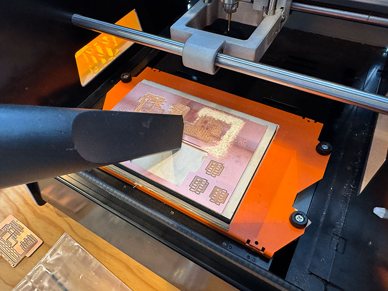
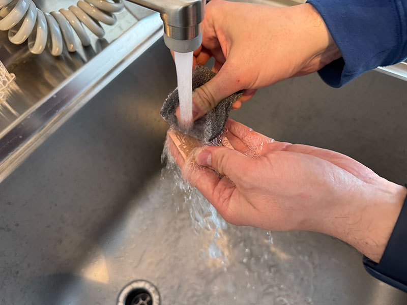
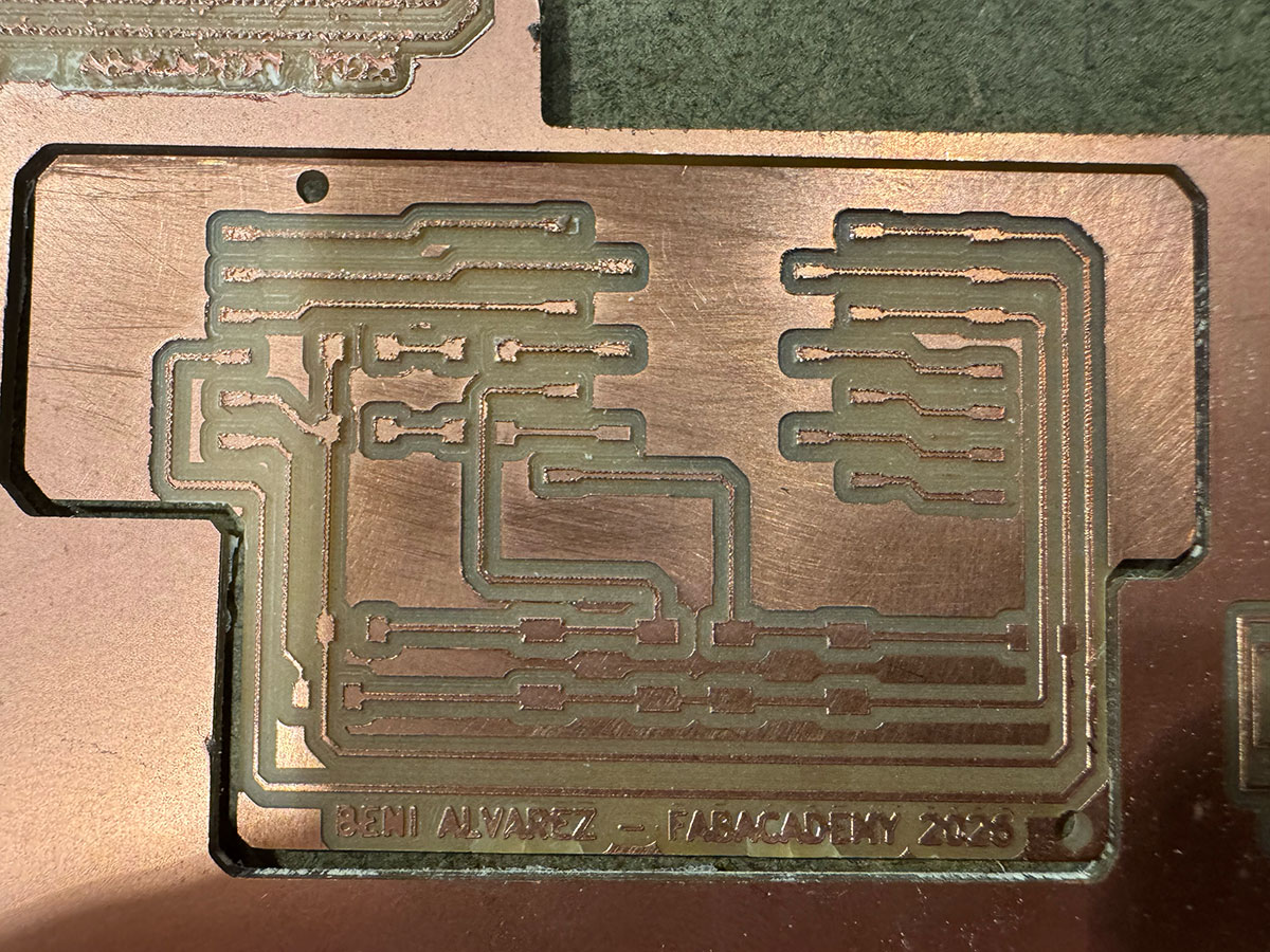
PCB cleaning and finishing
Once the milling process was finished, the next step was to clean the work area and prepare the board for use.
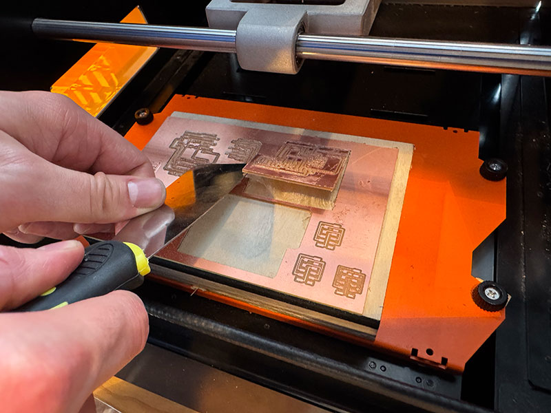
First, I vacuumed the milling debris, removing the dust and small material particles left on the machine surface. Then I removed the PCB from the sacrificial layer by gently levering it up with a spatula, taking care not to bend the board or damage the base surface.
After separating the board, I cleaned it more thoroughly using water and a steel wool pad. This step helps remove any remaining material that may not have been removed with the vacuum, as well as small burrs left around the traces or edges after machining.
Finally, I used a spatula to go over the edges of the PCB, slightly chamfering them to make them smoother. I also passed it over the front surface of the board to remove any burrs that might still have remained after the steel wool cleaning.
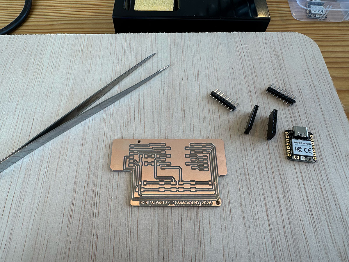
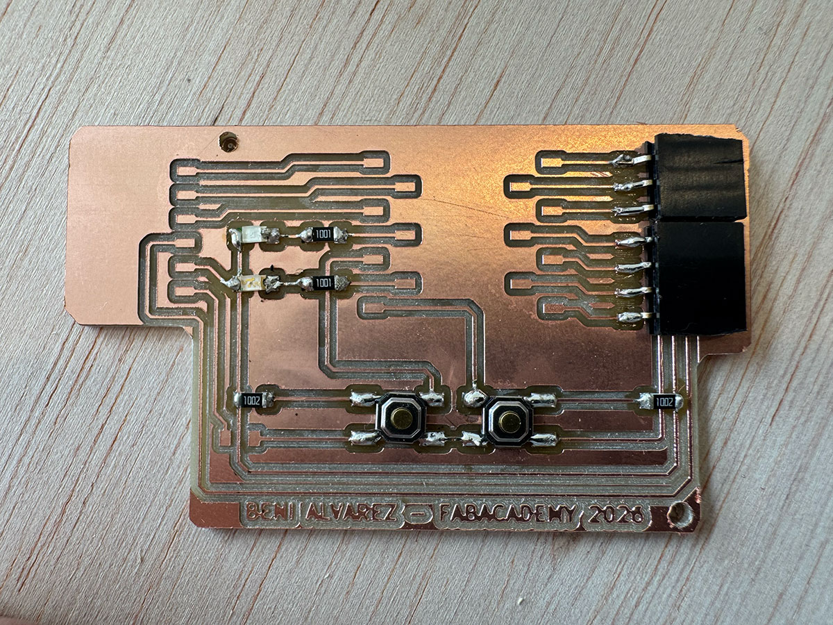
After this, the PCB was clean, smoother on the edges, and ready for the next step: component assembly.
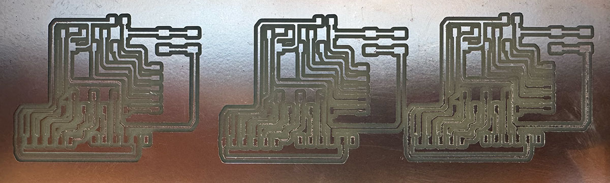
PCB final results
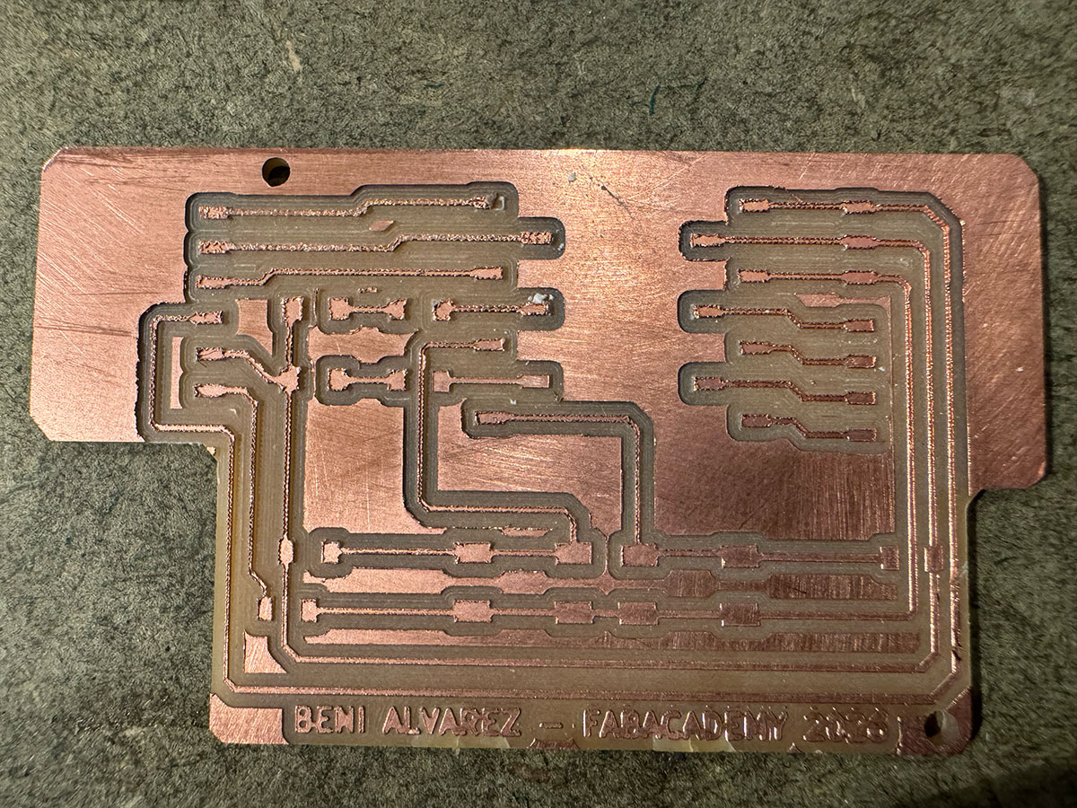
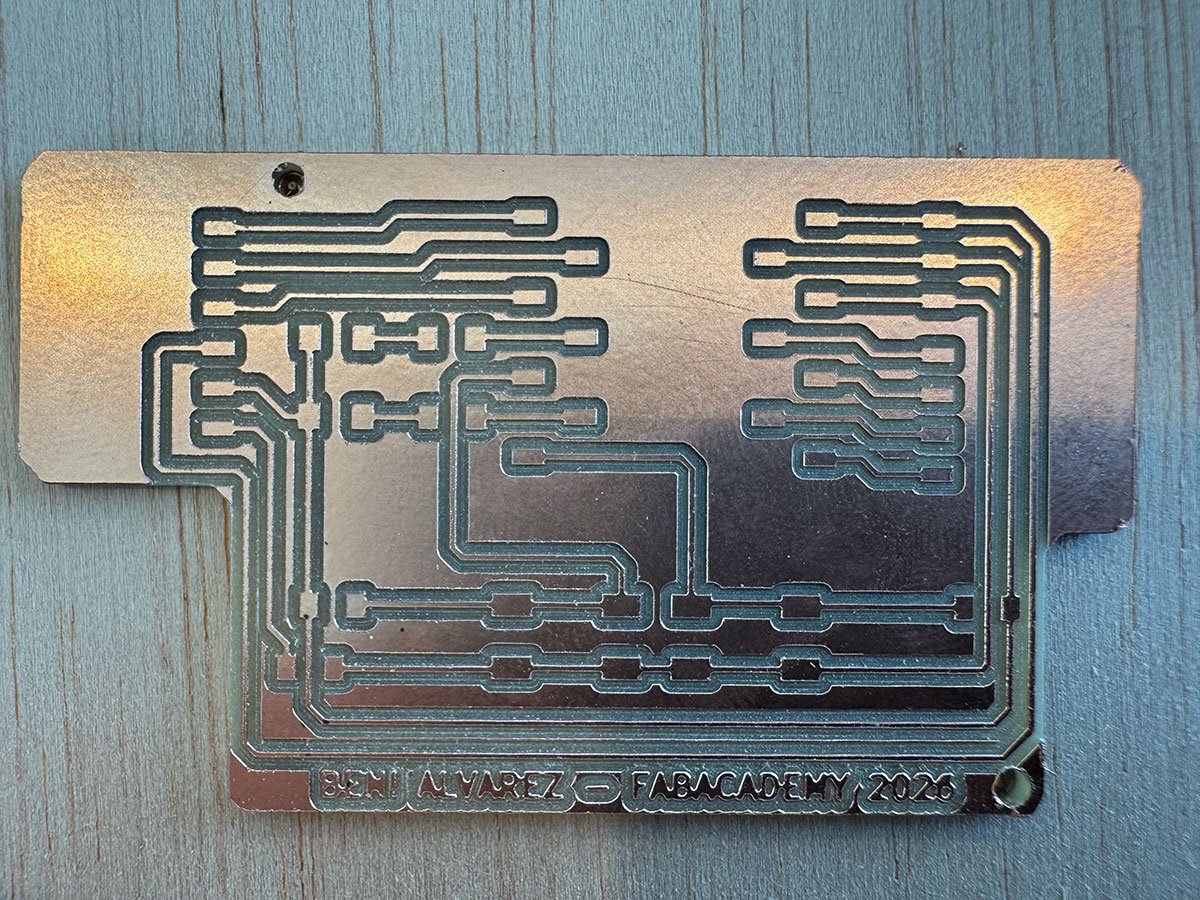
I decided to use Leon's backup to continue the process
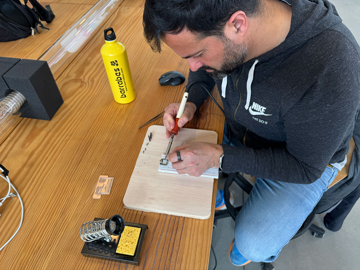
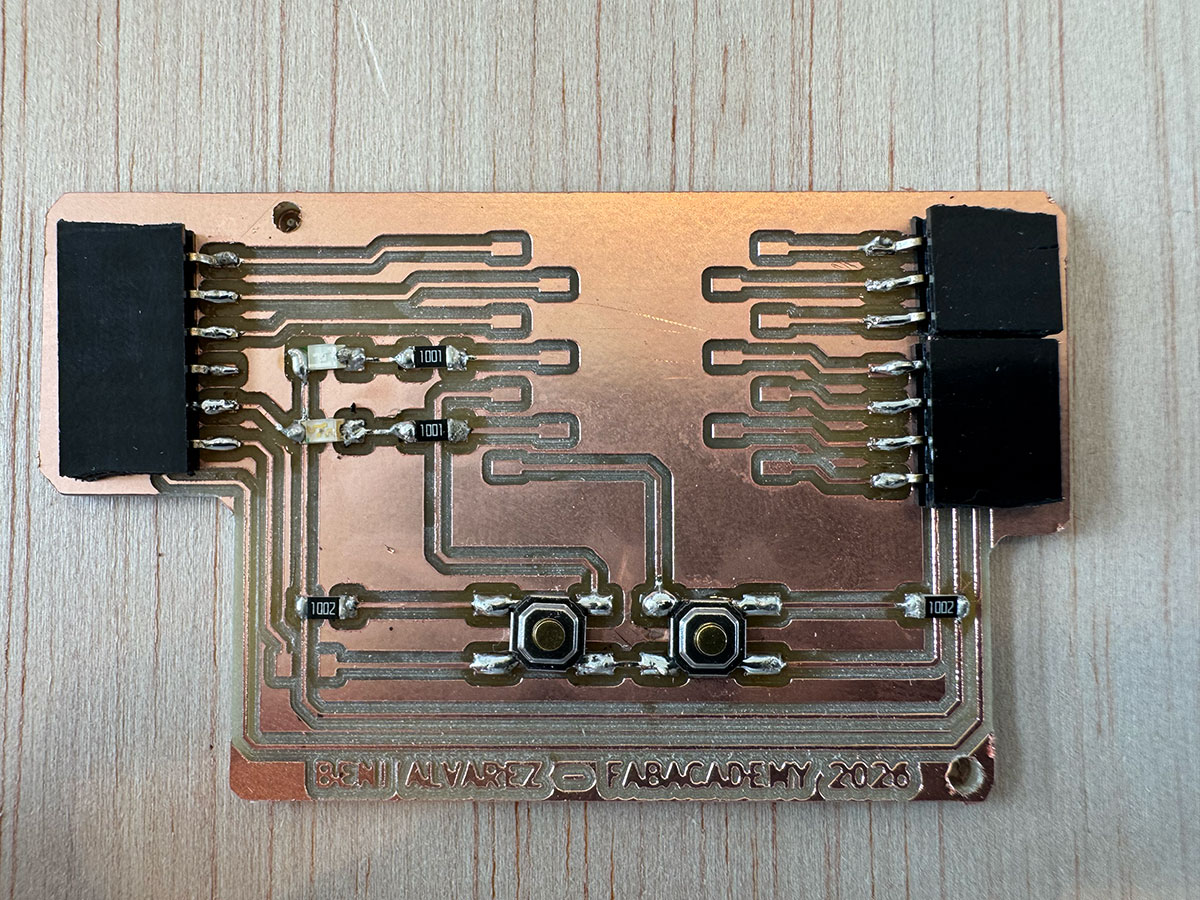
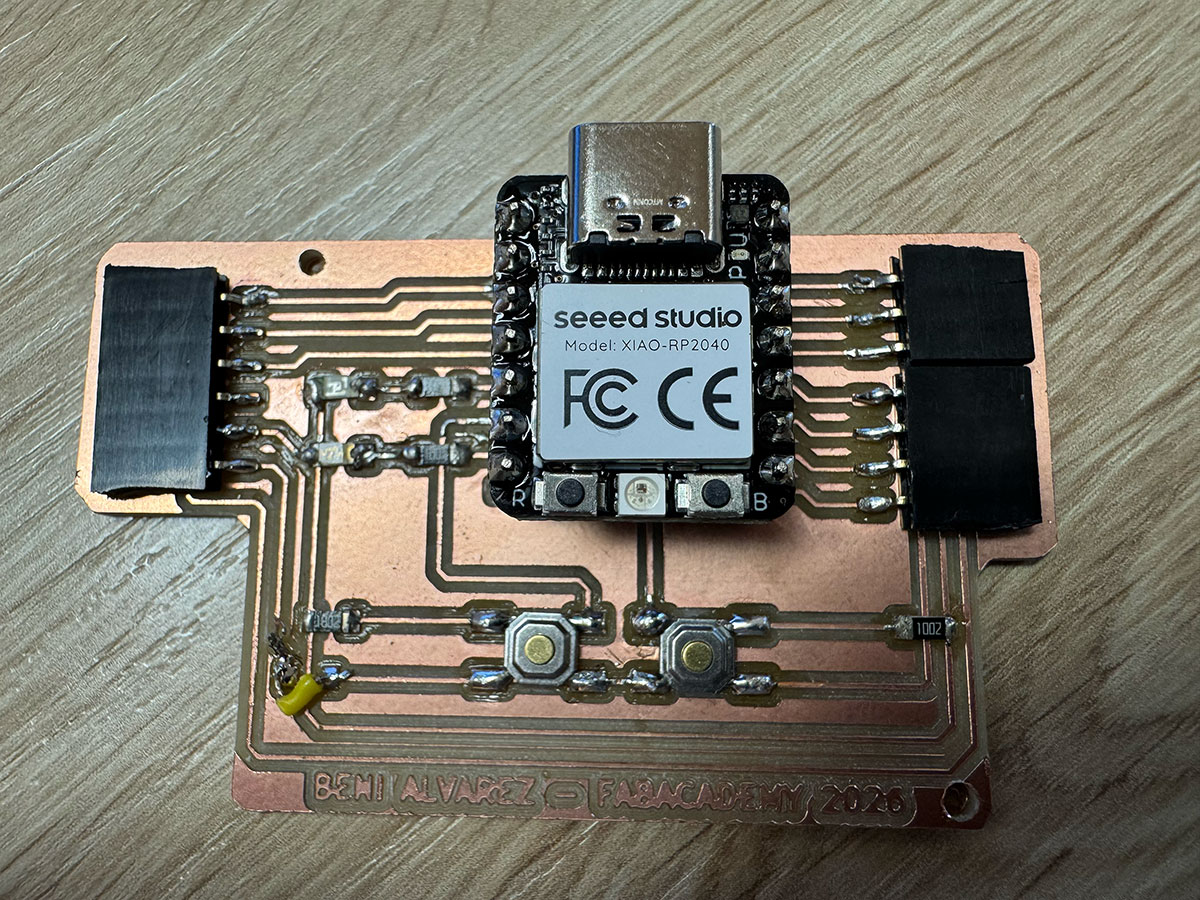
Soldering the components
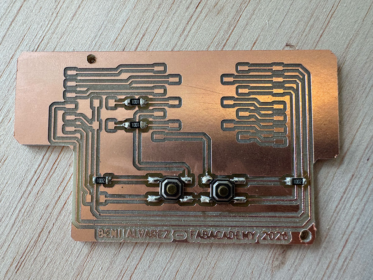
Once the PCB was ready (using FabLab León backup), the next step was to solder the electronic components onto the board.
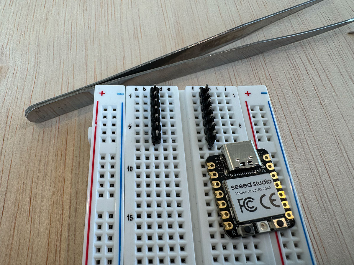
To make the assembly easier and avoid problems during the process, it is recommended to solder the components from the lowest profile to the tallest ones. This helps keep the board stable on the table while working. In my case, I followed this order: buttons, resistors, LEDs, pin headers, and finally the Xiao socket.
During soldering, it is important to use the right amount of solder. It should not be excessive, but it must be enough to ensure a good electrical contact and proper mechanical fixation of the component. A good indicator of a correct solder joint is the shiny appearance of the solder. When the surface looks dull or irregular, it usually means that the joint was not made properly.
The process I followed for soldering each component was the same. First, I placed a small amount of solder on one of the pads where the component would go. Then, using tweezers to position the component, I reheated that solder point and fixed the part in place. Once the component was correctly aligned, I proceeded to solder the remaining pins to complete the connection.
This method makes it easier to work with precision and helps prevent the components from moving while soldering.
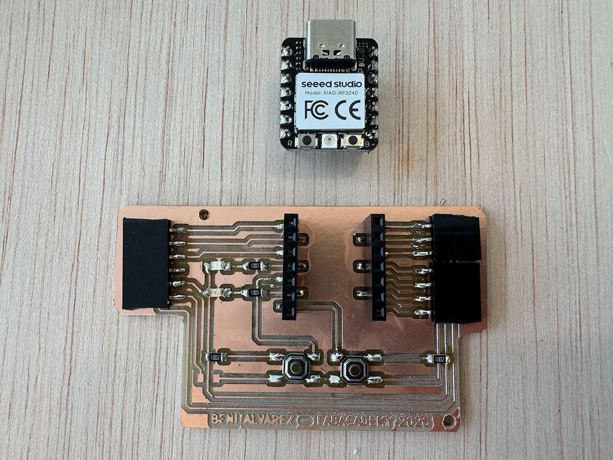
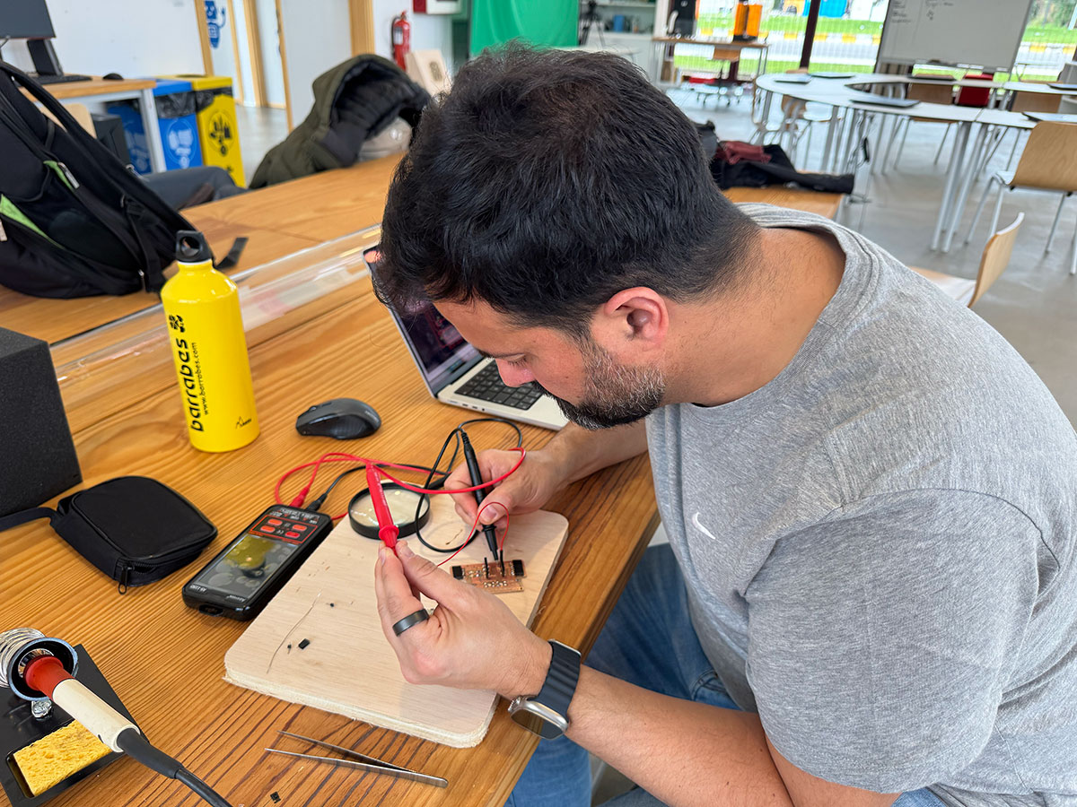
Programming and initial testing
The next step was programming the board to verify that everything worked correctly. I started with a simple test to check that the LEDs were working properly. For this, I used a basic blink program controlling both LEDs.
During this first test I encountered a problem. When programming the board in Arduino, I initially used the pin names corresponding to their physical labels on the Xiao board, programming them as 3 and 5. However, for Arduino these pins correspond to the internal numbers 29 and 7.
Before realizing this, I thought there might be a hardware issue with the PCB. To rule this out, I went back and carefully checked the continuity of the traces using a multimeter, looking for possible short circuits or unintended connections that might have occurred during soldering.
Once I identified the correct pin numbering (29 and 7), the issue was solved. After updating the code with the correct pin values, I was able to program the board successfully and confirm that the LEDs were functioning properly.
Test 1 · BeniPCBw08_test1.ino Show code
// FabAcademy 2026 - XIAO RP2040 LED test

const int LED1 = 29;
const int LED2 = 7;

void setup() {
  pinMode(LED1, OUTPUT);
  pinMode(LED2, OUTPUT);
}

void loop() {

  digitalWrite(LED1, HIGH);
  digitalWrite(LED2, LOW);
  delay(500);

  digitalWrite(LED1, LOW);
  digitalWrite(LED2, HIGH);
  delay(500);

}
For the second test, I programmed the board so that each of the two buttons controlled one LED. Each button press would toggle the corresponding LED on and off. This test allowed me to verify that both the input pins (buttons) and the output pins (LEDs) were working correctly.
Test 2 · BeniPCBw08_test2.ino Show code
// FabAcademy 2026 - XIAO RP2040
// Button1 toggles LED1
// Button2 toggles LED2

const int LED1 = 29;
const int LED2 = 7;

const int BUTTON1 = 0;
const int BUTTON2 = 6;

bool led1State = false;
bool led2State = false;

bool lastButton1 = HIGH;
bool lastButton2 = HIGH;

void setup() {

  pinMode(LED1, OUTPUT);
  pinMode(LED2, OUTPUT);

  pinMode(BUTTON1, INPUT);
  pinMode(BUTTON2, INPUT);

}

void loop() {

  bool button1 = digitalRead(BUTTON1);
  bool button2 = digitalRead(BUTTON2);

  // Detectar pulsación botón 1
  if (button1 == LOW && lastButton1 == HIGH) {
    led1State = !led1State;
    digitalWrite(LED1, led1State);
    delay(200); // debounce simple
  }

  // Detectar pulsación botón 2
  if (button2 == LOW && lastButton2 == HIGH) {
    led2State = !led2State;
    digitalWrite(LED2, led2State);
    delay(200);
  }

  lastButton1 = button1;
  lastButton2 = button2;

}
In the third test, I extended the program by adding an additional behavior. With each button press, the LED would cycle through three different states: turn on, blink, and turn off.
This small modification allowed me to test a slightly more complex logic in the program while confirming that the board was responding correctly to multiple input events.
Test 3 · BeniPCBw08_test3.ino Show code
// FabAcademy 2026 - XIAO RP2040
// Button cycles LED: OFF -> ON -> BLINK -> OFF

const int LED1 = 29;
const int LED2 = 7;

const int BUTTON1 = 0;
const int BUTTON2 = 6;

int stateLED1 = 0;
int stateLED2 = 0;

bool lastButton1 = HIGH;
bool lastButton2 = HIGH;

unsigned long previousMillis = 0;
const long blinkInterval = 500;

bool blinkState = LOW;

void setup() {

  pinMode(LED1, OUTPUT);
  pinMode(LED2, OUTPUT);

  pinMode(BUTTON1, INPUT);
  pinMode(BUTTON2, INPUT);

  digitalWrite(LED1, LOW);
  digitalWrite(LED2, LOW);

}

void loop() {

  bool button1 = digitalRead(BUTTON1);
  bool button2 = digitalRead(BUTTON2);

  // BUTTON1 cambia estado LED1
  if (button1 == LOW && lastButton1 == HIGH) {
    stateLED1++;
    if (stateLED1 > 2) stateLED1 = 0;
    delay(200);
  }

  // BUTTON2 cambia estado LED2
  if (button2 == LOW && lastButton2 == HIGH) {
    stateLED2++;
    if (stateLED2 > 2) stateLED2 = 0;
    delay(200);
  }

  lastButton1 = button1;
  lastButton2 = button2;

  // control blink
  unsigned long currentMillis = millis();
  if (currentMillis - previousMillis >= blinkInterval) {
    previousMillis = currentMillis;
    blinkState = !blinkState;
  }

  // LED1 comportamiento
  if (stateLED1 == 0) {
    digitalWrite(LED1, LOW);
  }
  else if (stateLED1 == 1) {
    digitalWrite(LED1, HIGH);
  }
  else if (stateLED1 == 2) {
    digitalWrite(LED1, blinkState);
  }

  // LED2 comportamiento
  if (stateLED2 == 0) {
    digitalWrite(LED2, LOW);
  }
  else if (stateLED2 == 1) {
    digitalWrite(LED2, HIGH);
  }
  else if (stateLED2 == 2) {
    digitalWrite(LED2, blinkState);
  }

}
Video test 1, 2 y 3:
High quality video available on my YouTube channel ↗️.
High quality video available on my YouTube channel ↗️.
High quality video available on my YouTube channel ↗️.
ROLAND SRM-20 Problems
Date: 17 March 2026
First tests
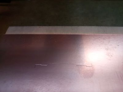
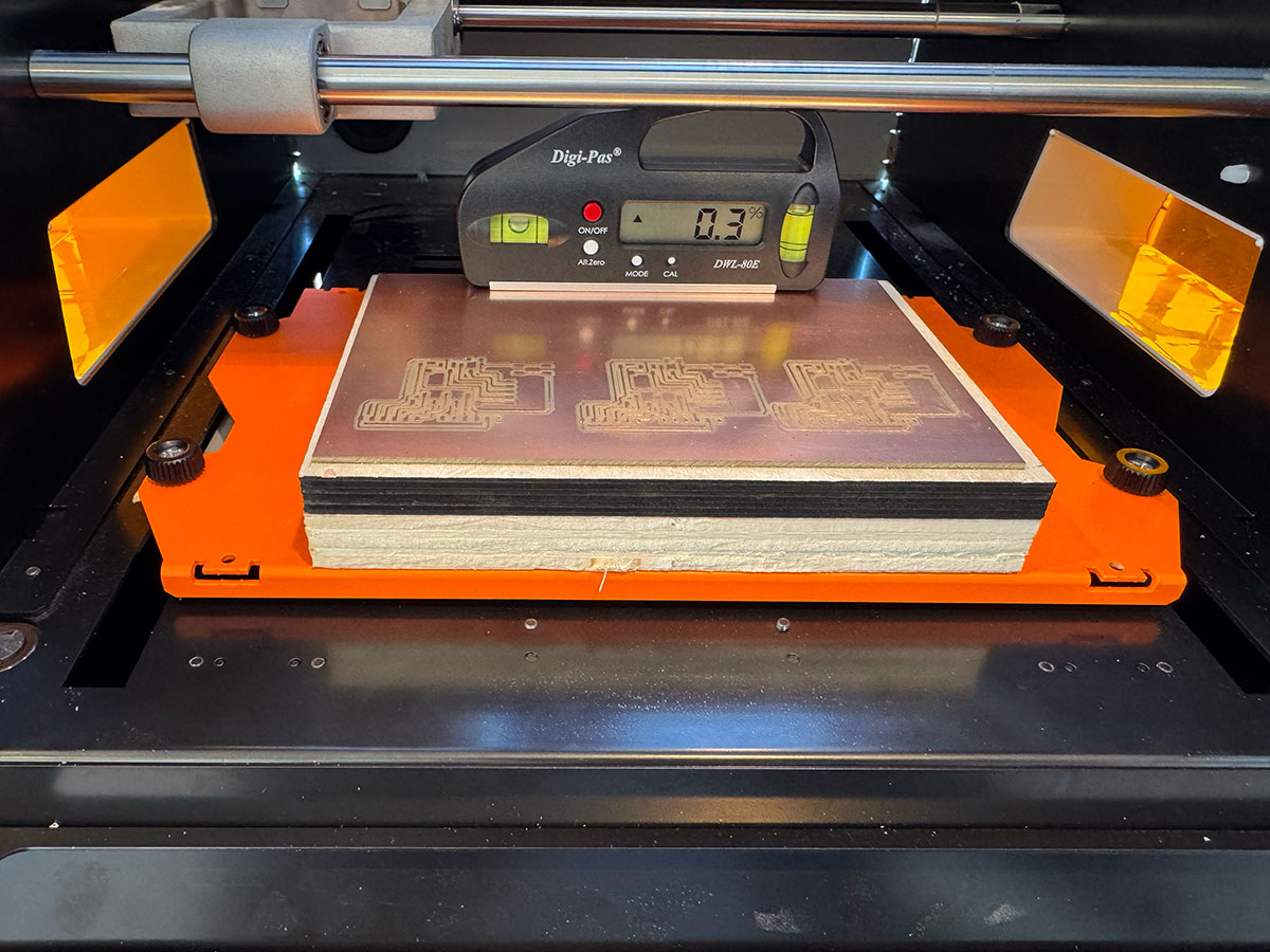
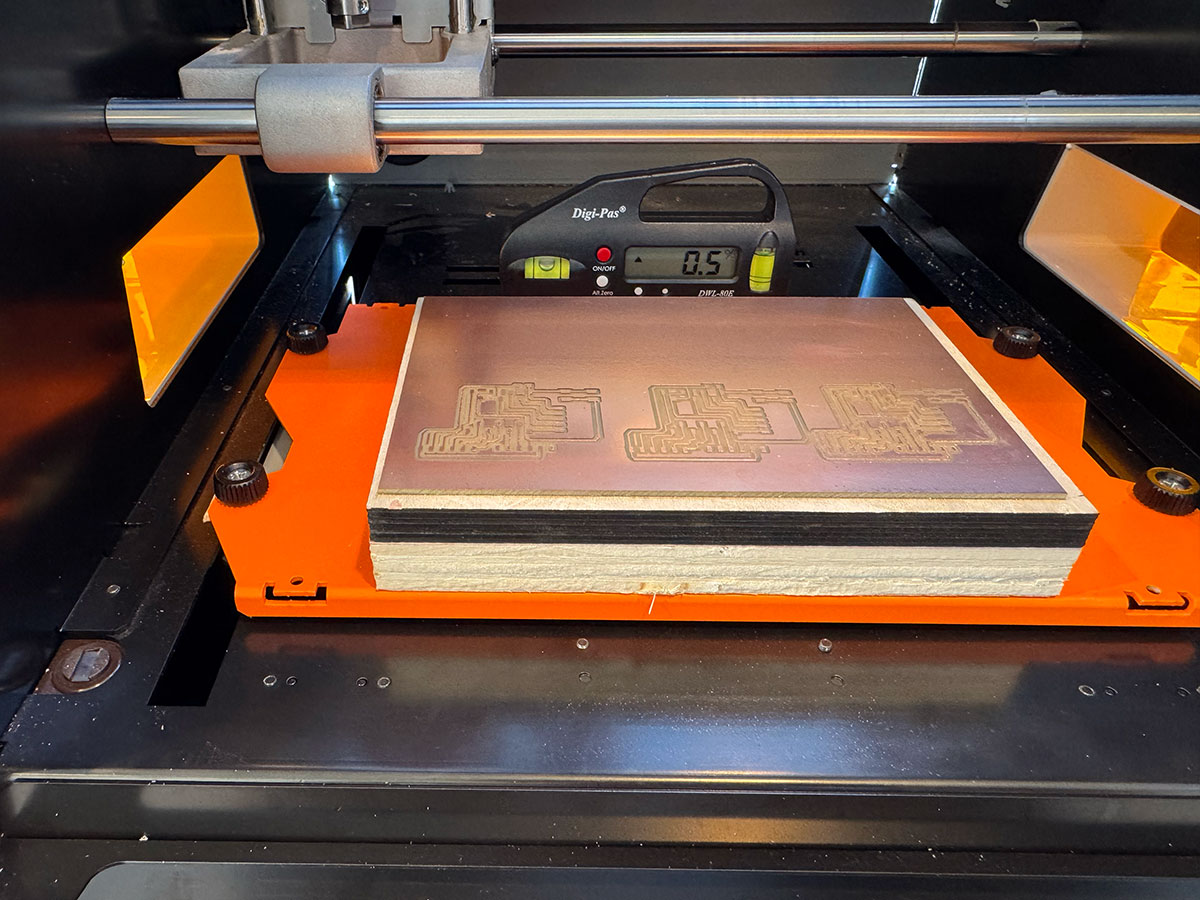
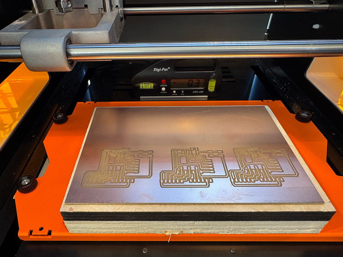
We started by adjusting XYZ and when processing the job we saw that the end mill didn't go down enough, so we adjusted Z=0 at a midpoint and processed the trace test.
Other Test
We have adjusted the leveling of the machine and the bed and replaced the base with a higher one.
We've continued testing and trying to determine if the finishing problems with the SRM-20 are due to adjustments, but although we've made some improvements, the machine isn't running smoothly. We've tried different adjustments, replaced the base, used different milling bits, made finer leveling adjustments, and tried different Z=0 settings, but the finish is still not right. These are the latest tests we've performed:
Y Axis levels:
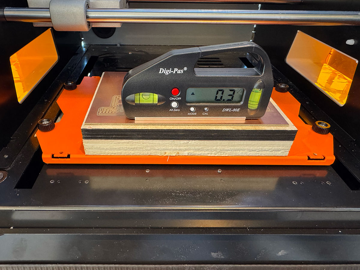
X Axis levels (both sides):
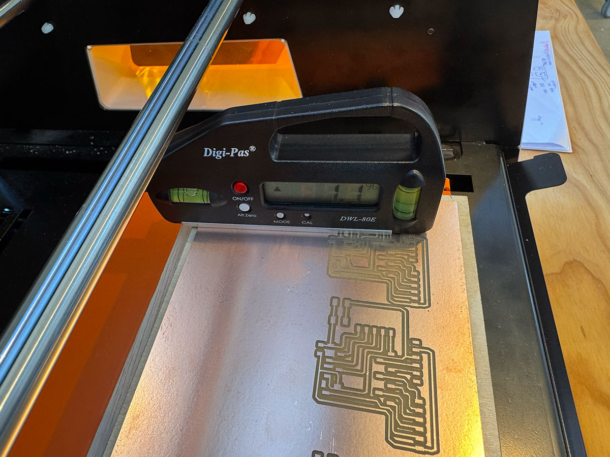
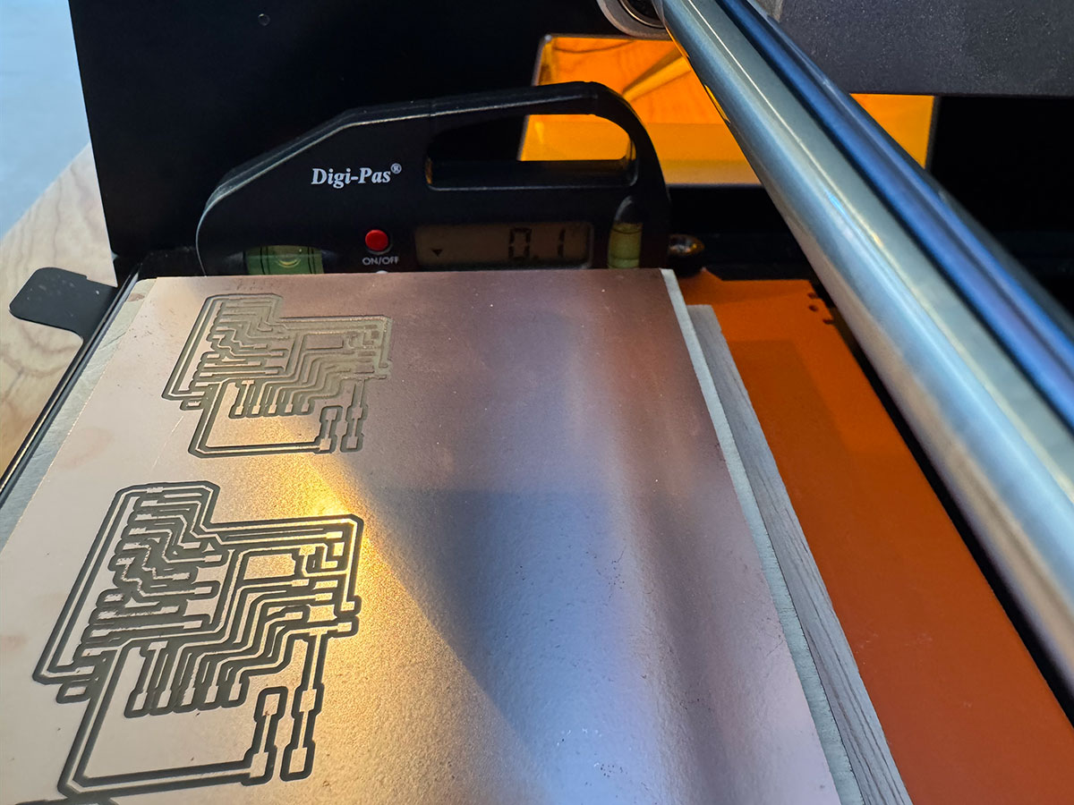
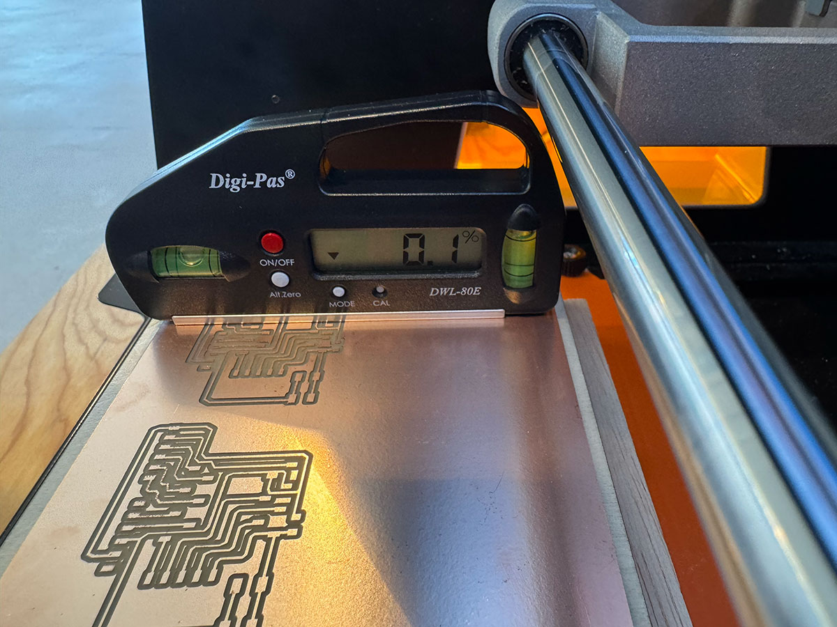
For finer adjustment of bed leveling, we have opted to add paper washers to achieve the most optimal level possible.
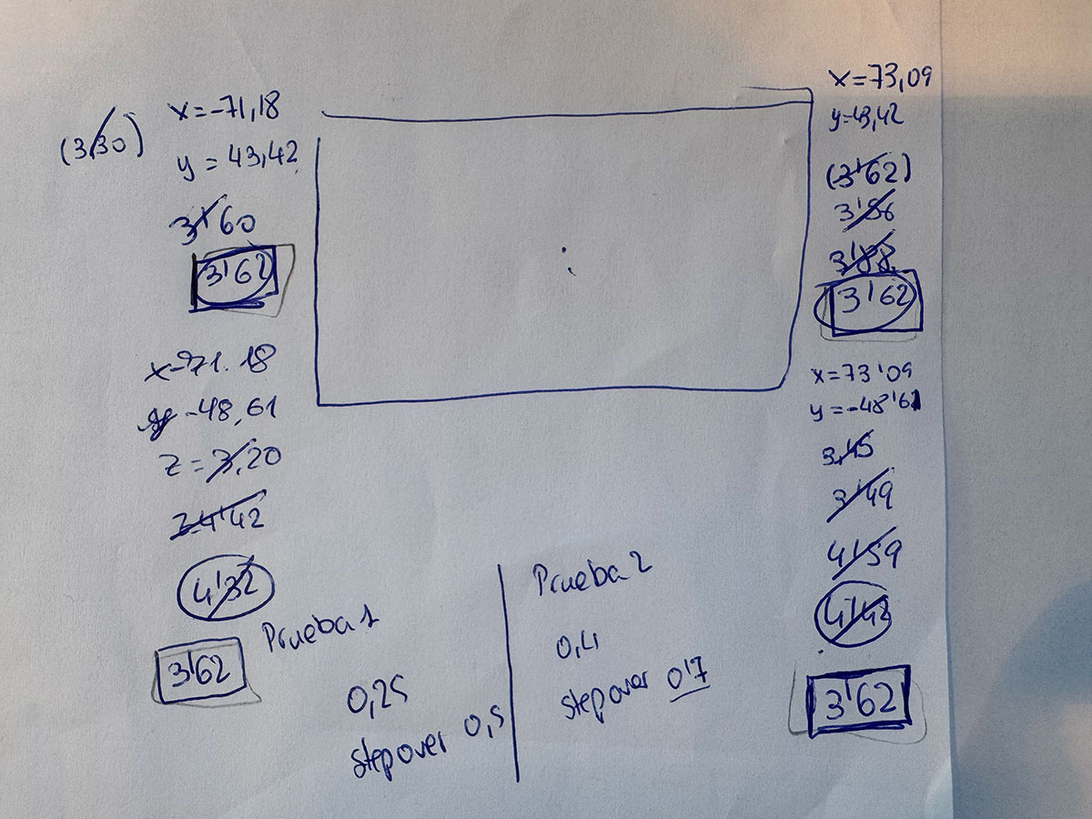
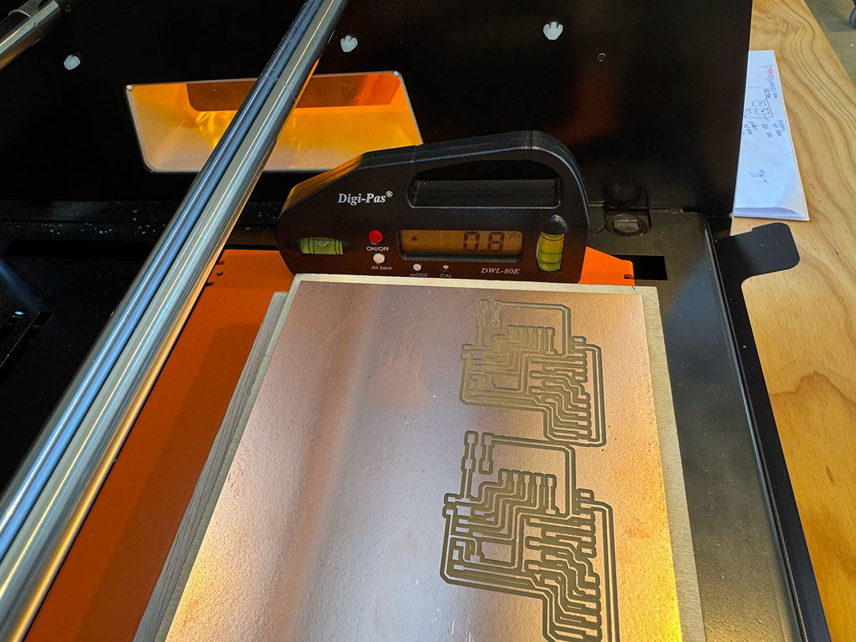
Lastest tests
These 3 tests were performed using a different mill end (see photo below) by changing the Z=0 point and the mill end insertion in the spindle.
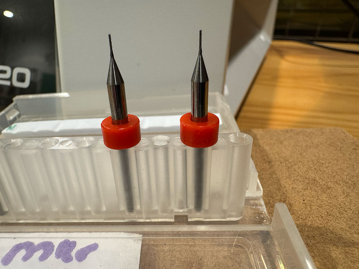
So far, we see a better result (test3) when Z=0 is in the middle and the end mill is inserted as far as possible into the spindle.
We have contacted the supplier and sent images and videos so that they can provide us with a possible solution, since the SRM-20 is new and there may be a manufacturing defect?.
High quality video available on my YouTube channel ↗️.
High quality video available on my YouTube channel ↗️.
Update: 24 March 2026
After opening a support ticket with the seller, we have sent the Roland SRM-20 today for them to evaluate the problem and fix it within the warranty period.
Update: 16 April 2026
We received the SRM20 with the spindle bearings replaced. We performed a line test and the result is quite good, especially compared to the same test performed a few weeks ago.
Update: 24 april 2026
This week in Moulding and Casting, after successfully completing sample PCB trace tests a few days ago, we attempted to make wax molds and encountered problems from the start.
As soon as the endmill tried to engage and remove wax, it lacked power and the machine stopped. We observed that the spindle speed didn't exceed 2500 rpm when it should reach approximately 9000 rpm.
In the trace tests, the spindle reached 5000 rpm, and since that was the correct result, we initially thought that after replacing the bearings, the problem was with the spindle's rpm sensor.
However, today, after seeing the results and the issues, we contacted the supplier again and have to send the machine back so they can presumably replace the spindle with a new one.
Original code files for this documentation
Files for download
- Gerber files (PCB.zip) ZIP · 16 Kb
- PNG files (PCB_pngs.zip) ZIP · 77 Kb
- RML oland toolpath files -Traces, Drills & Outside (RMLtoolpaths.zip) ZIP · 26 Kb
- Arduino code test 1 (BeniPCBw08_test1.ino) INO · 1 Kb
- Arduino code test 2 (BeniPCBw08_test2.ino) INO · 1 Kb
- Arduino code test 3 (BeniPCBw08_test2.ino) INO · 2 Kb
Week questions/tasks
Final reflection
It's been a week of many new developments and a lot of work, but the effort and dedication have paid off. Seeing an LED blink or respond to a button press on a PCB you designed, manufactured, soldered, and programmed yourself is incredible.
These have definitely been weeks of constant evolution, and you're really aware of it.
Credits
I would like to thank the instructors Nuria ↗️, Pablo ↗️, and Adrián ↗️ for their guidance and support throughout this assignment.
Also thanks to Javier ↗️ (FabLab Ponferrada Manager) for facilitating our access to the fablab and training us in the use of the machines.
I am also grateful to my FabAcademy’26 León group mates — Efrén ↗️, Íñigo ↗️, and Óscar ↗️ — for sharing knowledge, ideas, and troubleshooting together, making the learning process more collaborative and enriching.
All texts were written in Spanish and translated into English using Google Translate and ChatGPT.