Week 6
Electronics Design
Contents
Week questions/tasks
Starting Point
This week was, honestly, a pretty big leap for me.
Up to now, my contact with electricity and electronics had been very superficial. I was familiar with concepts like DC and AC, voltages, polarities, and circuits… but more as “words I’ve heard” than something I truly understood in depth.
My previous experience was basically limited to using a multimeter: checking continuity in a cable, or measuring whether there was voltage present (12V, 240V…) to confirm if there was power or not. Not much beyond that.
I understood that electricity flows through a circuit, but I didn’t really know what role each component plays. An LED was just an LED. A resistor was something that “reduces” something. A capacitor… that’s where the fog really started.
So this week became a personal challenge. It wasn’t only about designing a PCB, but about starting to understand—at least at a very basic level—what each component does, why it is there, and what I should be measuring if everything is working correctly.
More than a design week, for me it felt like a week of building foundations.
Group assignment
Use the test equipment in your lab to observe the operation of a microcontroller circuit board (as a minimum, you should demonstrate the use of a logic analyzer)
Multimeter
As part of this process of starting to understand electronics from the ground up, I decided to upgrade one essential tool: the multimeter.
The one I had was quite old (a friend had given it to me years ago), and the cables were already close to breaking. It still worked… but it didn’t inspire much confidence.
So I bought a new one on Amazon. It’s not a professional lab-grade device, but for learning and performing basic measurements, it’s more than enough.
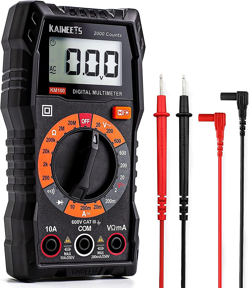
Basic specifications
| Function | Specification |
|---|---|
| Auto-range | Manual range selection |
| AC Voltage | 20V / 200V / 600V |
| DC Voltage | 200mV / 2V / 20V / 200V / 600V |
| DC/AC Current | 20m / 200m / 10A |
| Frequency | — |
| Resistance | 200Ω / 2kΩ / 20kΩ / 200kΩ / 2MΩ / 20MΩ |
| Capacitance | — |
| NCV | — |
It’s not the most advanced multimeter in the world, but it covers the essentials: voltage, continuity, and resistance — exactly what I needed this week.
To make sure I was actually understanding what I was doing (and not just placing the probes and waiting for numbers to appear), I followed a YouTube tutorial by Adrián Torres about how to use a multimeter. It helped me better understand what each mode measures and how to position the probes correctly.
Measurements performed
With the new multimeter, I started running different tests to get familiar not only with the tool itself, but with what the measurements actually mean.
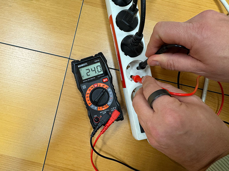
Voltage measurement (AC and DC)
First, I measured voltage in both alternating current (AC) and direct current (DC).
- I measured a home wall socket (AC).
- I measured a variable power supply at the FabLab (DC).
Beyond just reading the number on the screen, the interesting part was understanding the practical difference between AC and DC measurements, and how the selector on the multimeter changes depending on what I want to test.
Continuity measurement
Next, I tested continuity.
I used the QPAD-Xiao board to check different points in the circuit. First, I verified continuity on GND, and then on several of the touchpad traces.
Here the learning was very clear: it’s not only about seeing a value on the screen, but also about hearing the well-known “beep” that indicates continuity between the two measured points.
That small sound gives a lot of reassurance when checking whether a trace is properly connected or if there is a break somewhere.
High quality video available on my YouTube channel ↗️.
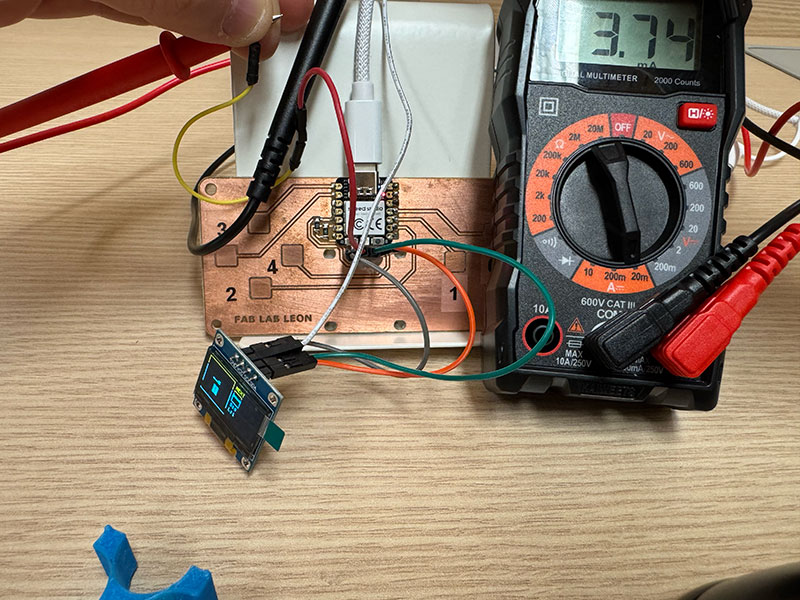
Current measurement
Still working with the QPAD-Xiao, I then measured the current consumption of the display.
To do this, I disconnected the display and created bridges on the four pins (GND, VCC, SCL, and SDA), leaving VCC open so I could insert the multimeter in series and measure the current properly, always respecting the direction of flow.
This helped me understand something important: measuring current is not the same as measuring voltage. You can’t simply touch two points — you have to break the circuit and place the multimeter as part of the current path.
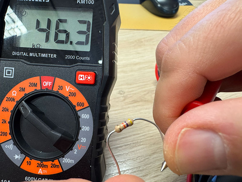
Resistance measurement
Using a resistor from the FabLab, I performed a simple check to measure its actual value.
In this case, the resistor was 47kΩ, and the measured value matched the expected one. It’s a basic test, but it really helps connect the color bands on the component with the numerical value shown on the screen.
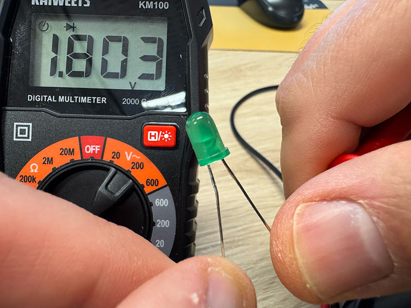
Diode / LED polarity test
Finally, I tested the diode function (the “->|” mode).
I placed the probes respecting polarity:
- Short leg → negative
- Long leg → positive
When running the test, a value appeared on the display, indicating the forward voltage drop of the LED.
In this case, the LED did not visibly light up, probably because the multimeter does not supply enough current to make it glow. Still, it was interesting to see how the device allows you to verify whether the diode is working and correctly oriented.
Logic analizer
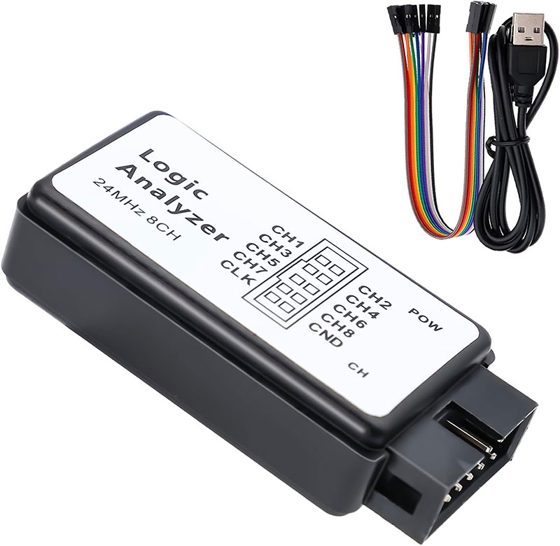
Besides the multimeter, this week was also my first real contact with a logic analyzer.
At the FabLab we have a Binghe 8-channel Logic Analyzer, so I decided to take the opportunity to better understand what digital communication actually looks like “from the inside”, instead of just knowing that it exists.
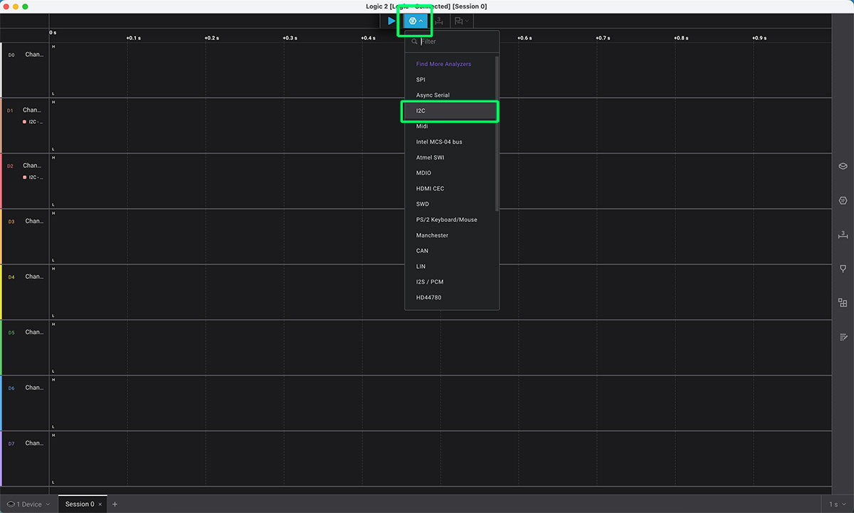
To use it, I first downloaded the Saleae Logic software, which allows you to visualize and analyze the signals captured by the analyzer.
Analyzing I2C communication
My goal was to observe the I2C communication between the QPAD-Xiao and its display.
To do this, I removed the screen and connected the pins GND, SCL, and SDA to the logic analyzer. The idea was to capture the signal directly from the bus and visualize how data is actually transmitted.
Once connected via USB, the software automatically recognized the analyzer. Inside the application, I selected the I2C protocol and configured the channels as follows:
- CH1 → SCL
- CH2 → SDA
With everything ready, I pressed PLAY to start capturing.
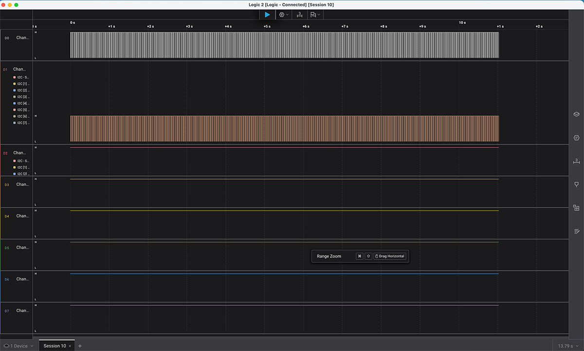
The timeline immediately showed the digital signals moving in real time. At first, it looks a bit chaotic if you’re not exactly sure what you’re looking at, but little by little you start recognizing patterns.
After stopping the capture, I checked the analyzed time span and began zooming into the signal. When zooming in, I could clearly see that not all transmissions had the same duration: there were differences in packet lengths and in the timing between signals.
That moment was particularly interesting, because I2C communication stopped being something abstract. It was no longer just “two wires sending data” — it became a real sequence of pulses that I could see, measure, and analyze.
High quality video available on my YouTube channel ↗️.
Document your work on the group work page and reflect what you learned on your individual page
This week, group work has been important for me, as I've benefited from my classmates' knowledge and explanations to understand electricity and circuits (at a basic or lower level). We've conducted tests and measurements, which we've then individually documented in our reports.
Individual assignment
Use an EDA tool to design a development board that uses parts from the inventory to interact and communicate with an embedded microcontroller
For this week (Electronic Design), my goal for the individual assignment was to design a small development board using an embedded microcontroller and parts from the Fab Academy inventory, and to bring the design to a point where it is ready to be fabricated (or at least properly checked and documented). In my case, I completed the full workflow with KiCad.
Installation and setup
First, I downloaded KiCad from the official website. I went to the download page and chose the macOS version, selecting the Europe / CERN build. Once installed, KiCad was running smoothly.
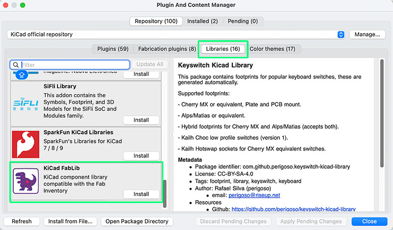
Then, to work directly with Fab Academy–compatible parts, I added the Fab library by following Krisjanis Rijnieks tutorial. This saved me a lot of time because the symbols and footprints are already prepared for the kind of boards and components we use in the lab.
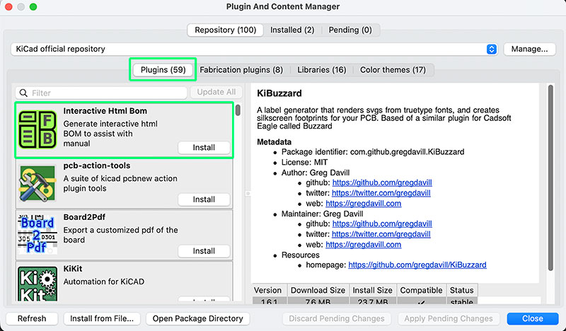
As an extra, I also installed the “Interactive HTML BOM” plugin, which later helped me generate a very convenient interactive BOM (and it’s great for documentation too).
To get comfortable with the tool, I relied on the official KiCad documentation—mainly to learn the basics of each editor and where the key options are. With that, I was ready to start.
Creating a new KiCad project
Next, I created a new project. KiCad automatically generates the main files:
*.kicad_pcb(PCB Editor)*.kicad_sch(Schematic Editor)
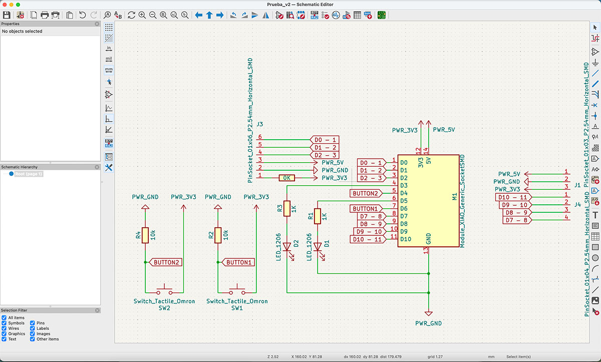
Schematic design (Schematic Editor)
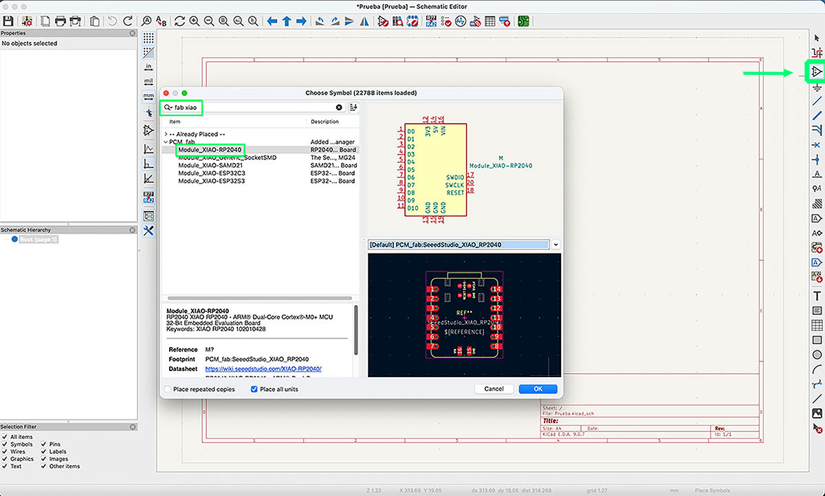
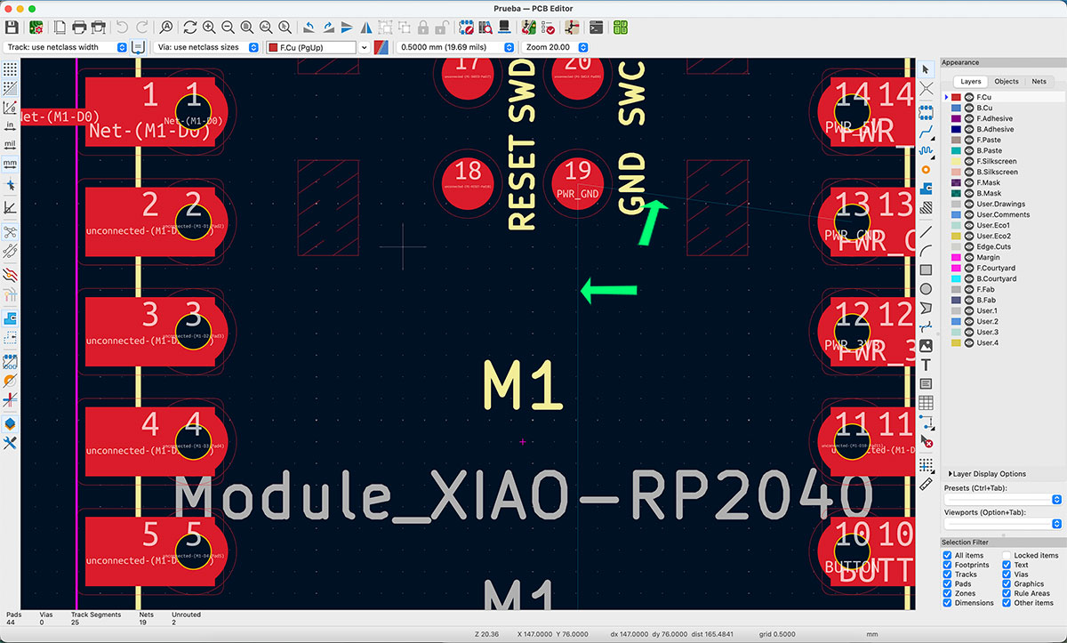
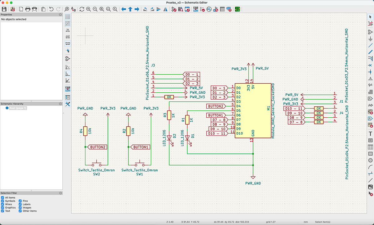
I opened the Schematic Editor file and started adding components from the Fab Academy inventory using “Place Symbols”. This opens a window with all available libraries. The key trick here was simple: in the search field I typed “fab” to filter the results and show only the Fab Academy inventory.
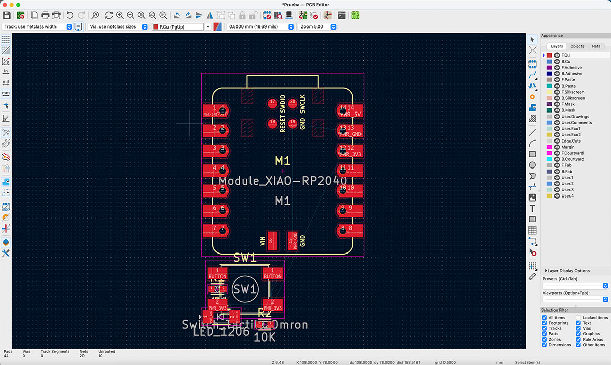
For example, to add the XIAO-RP2040, I used a filter like “fab xiao”, selected it from the results, and KiCad immediately provided both the symbol and the footprint, which is exactly what I wanted (no manual matching needed).
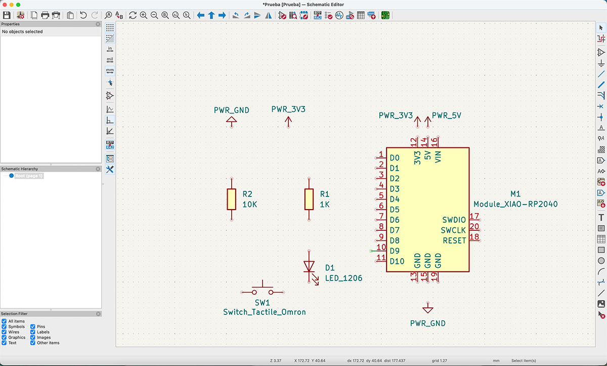
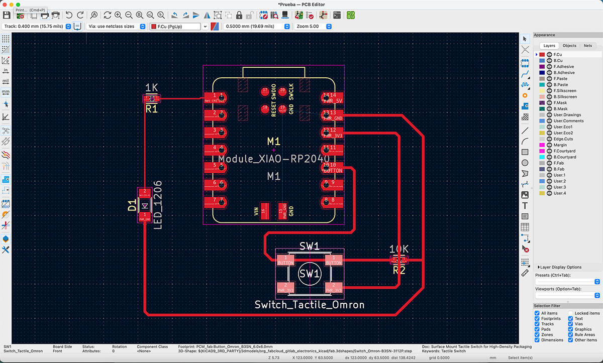
For this first circuit, I added:
- Module XIAO RP2040
- Power symbols: 3V3, 5V and GND
- LED_1206
- Switch_Tactile_Omron
- 2 × R_1206 resistors (one for the button and one for the LED)
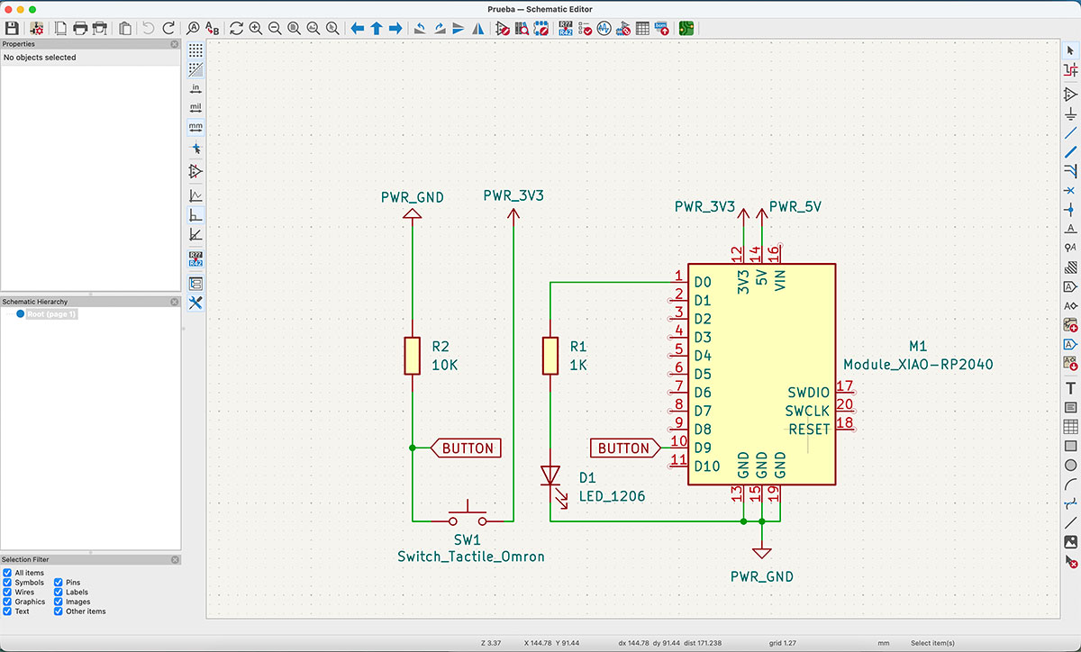
Once the components were placed, I began drawing the connections using “Draw Wires”, moving the symbols around the workspace to keep everything readable. This helps a lot later when switching to PCB, because the layout is clearer and easier to follow.
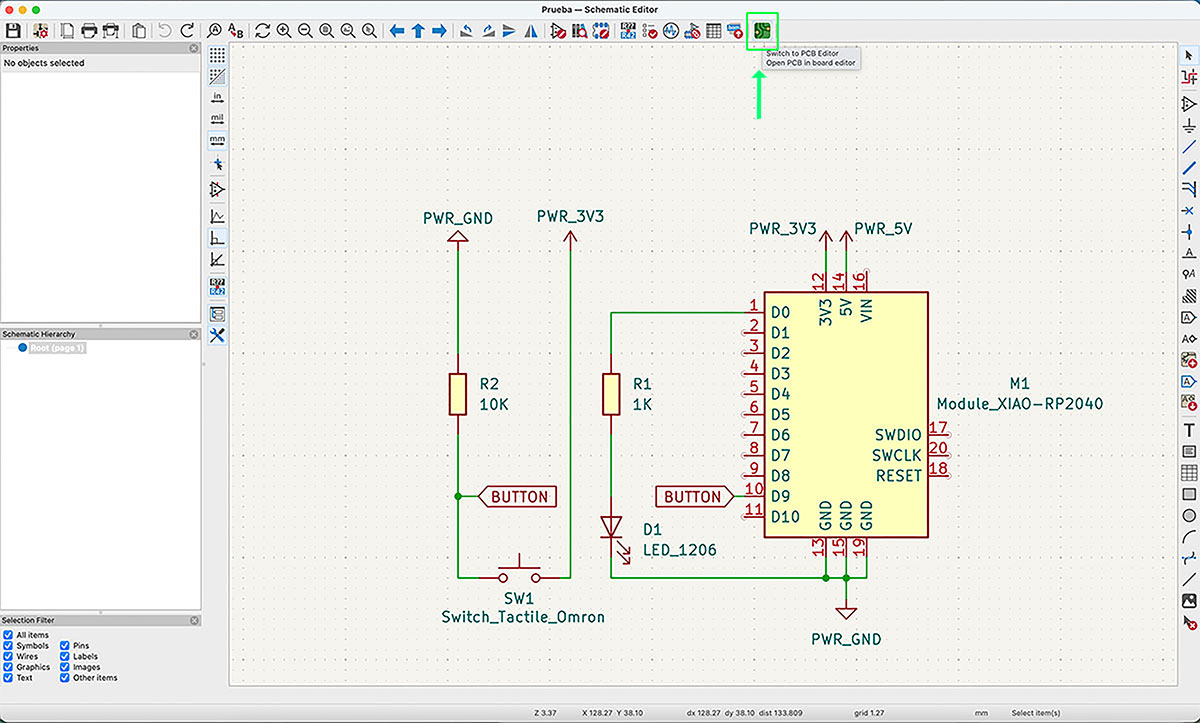
Switching to PCB and updating from the schematic
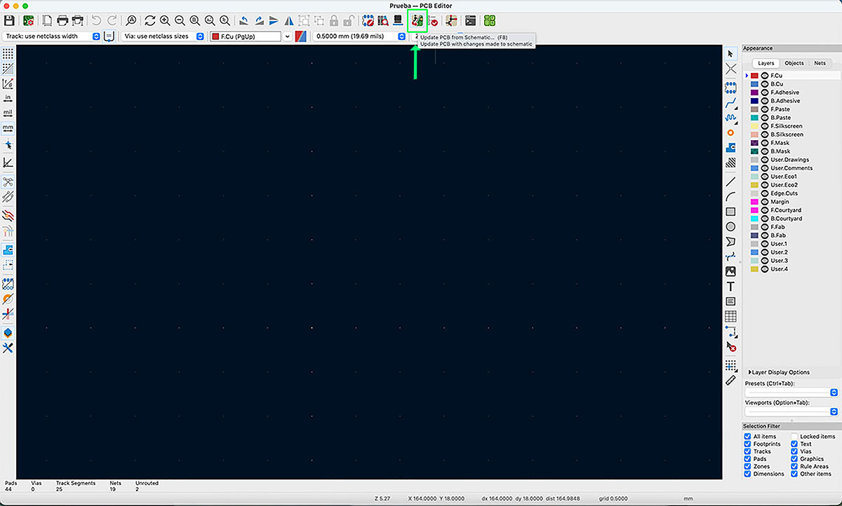
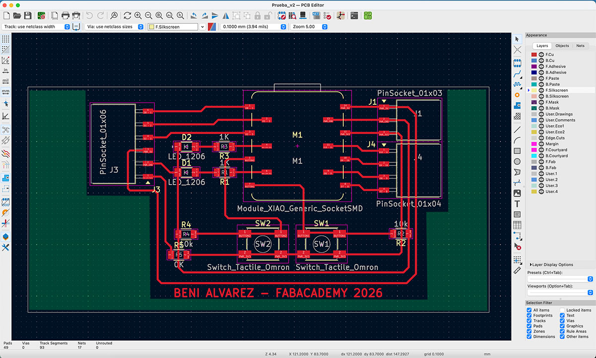
With the schematic finished, I moved to the PCB layout by clicking “Switch to PCB Editor”. Inside the PCB editor, I used “Update PCB from Schematic” to import all the components into the board.
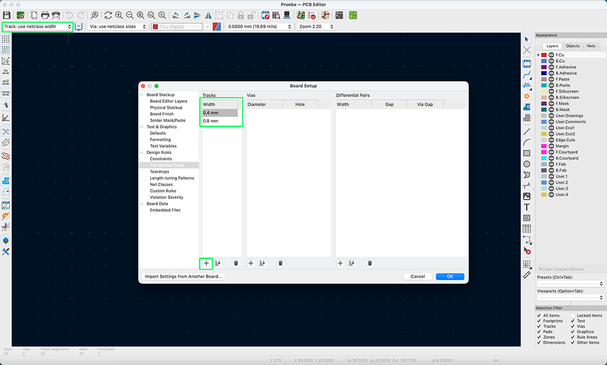
Before routing, I defined track widths by opening “Edit predefined Sizes” and adding two values: 0.4 mm and 0.8 mm. In this design I didn’t really need 0.8 mm, but I preferred to have it ready in case I wanted a thicker track for power or critical areas.
Component placement and routing
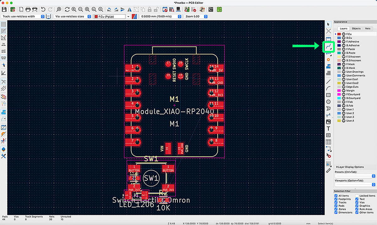
This is where the “hands-on” part starts: I placed the parts on the PCB and began connecting them by drawing tracks with “Route single track”.
I routed all traces on the red layer “F.Cu” (front copper). A super helpful feature in KiCad is that, after importing the schematic, it shows thin blue lines (airwires) suggesting which pads should be connected based on the schematic. They are not real traces, but they guide you and help make sure you don’t forget any connection.
While routing, I followed a common rule: avoid 90° angles because they can become problematic points (and they’re generally bad practice). So I kept corners at 45°, which the routing tool supports easily.
With that in mind, I completed all the traces.
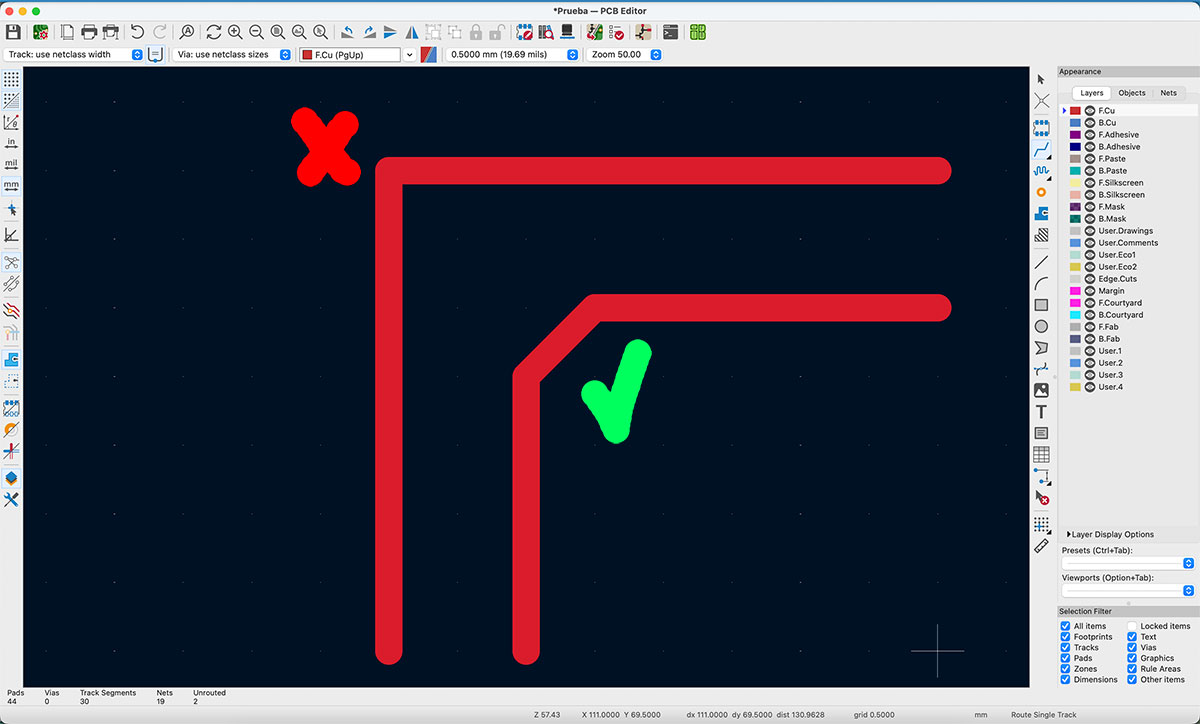
Avoiding trace crossings and cleaning up the layout
At one point, to connect everything without crossing traces, I had to use one of the resistors as a jumper (basically to “bridge” over a conflict). It worked as a quick solution to understand the bottleneck… but I wasn’t happy with that as a final result.
So I went back, repositioned the components, and rerouted the traces to avoid the crossing without relying on that workaround. This gave me a cleaner, more logical design that will also be easier to fabricate and review.
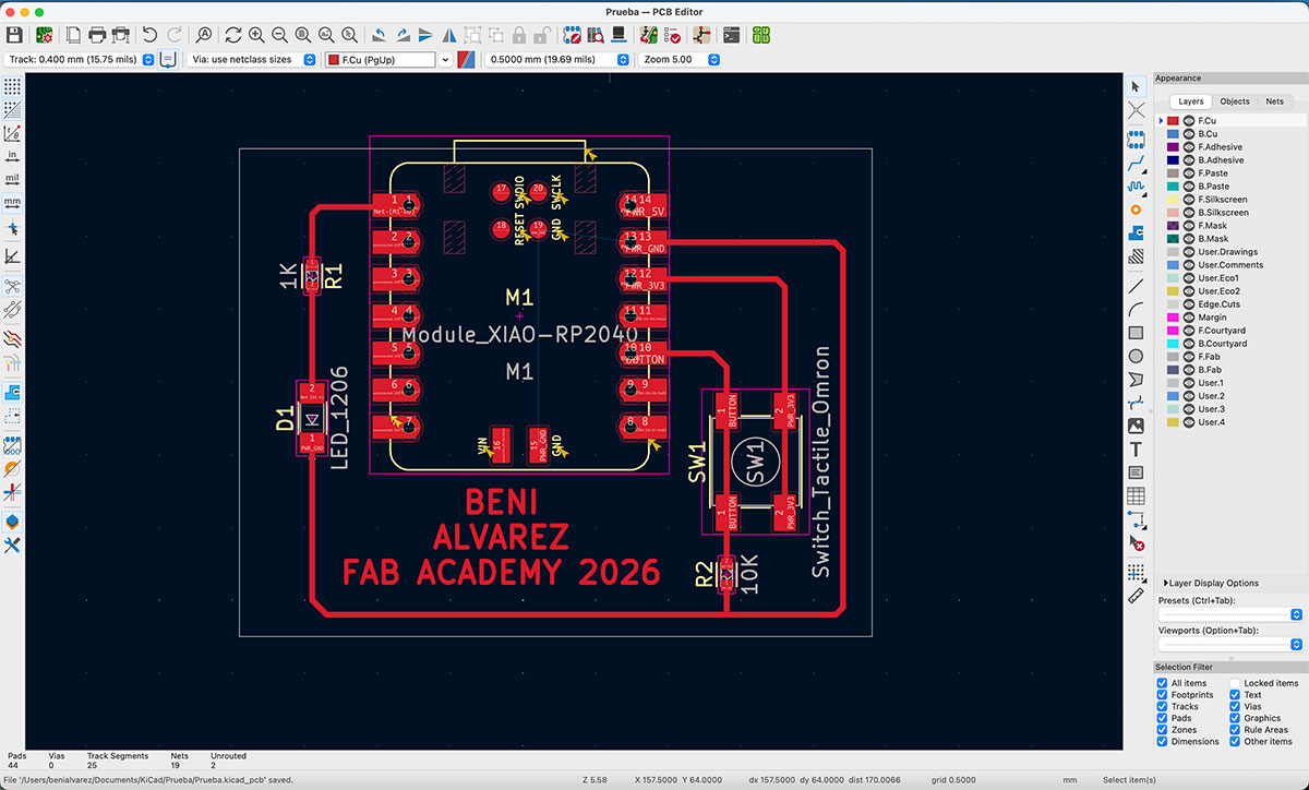
Once the layout was clean:
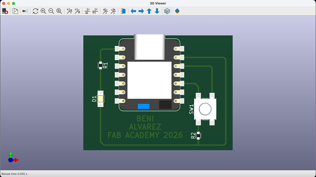
- On the “Edge.Cuts” layer (light gray), I drew the rectangle that defines the PCB outline.
- I also added a text label with my name and a reference to this Fab Academy work.
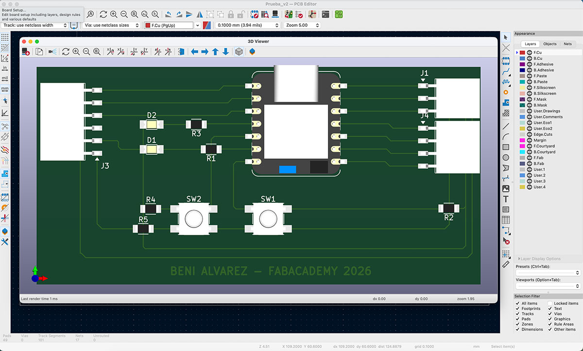
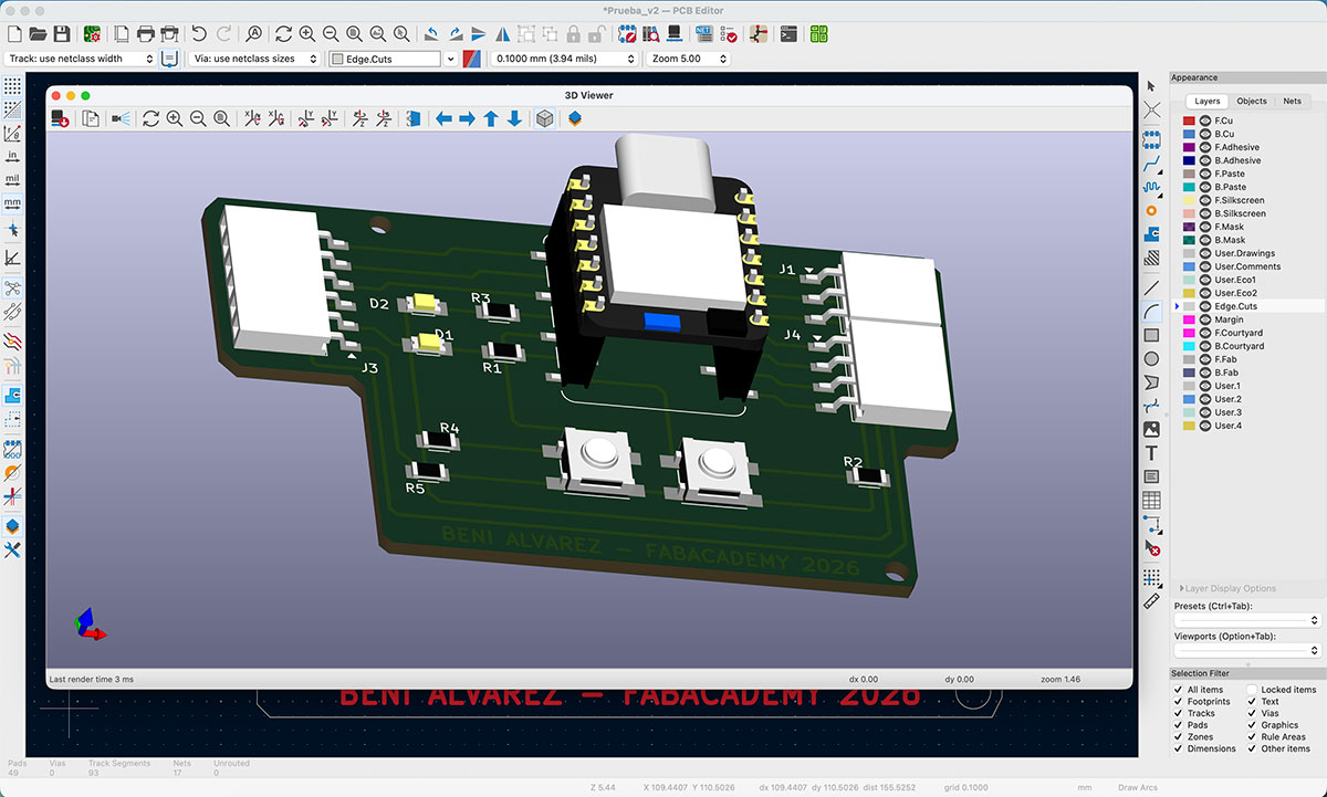
As a final visual check, I opened the 3D view via “View” → “3D Viewer” to confirm that the placement and overall result made sense.
Interactive BOM (HTML)
With the plugin installed from the start, I generated the interactive BOM by clicking “Generate Interactive HTML BOM”. This creates an HTML file where you can explore the parts list and highlight each component directly on the board—very handy both for assembly and for documentation.
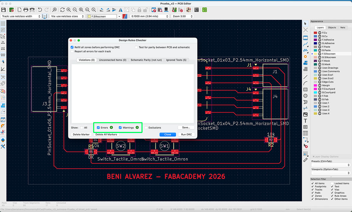
Prueba_v1.1.html BOMDesign Rules Checker (DRC): errors and warnings
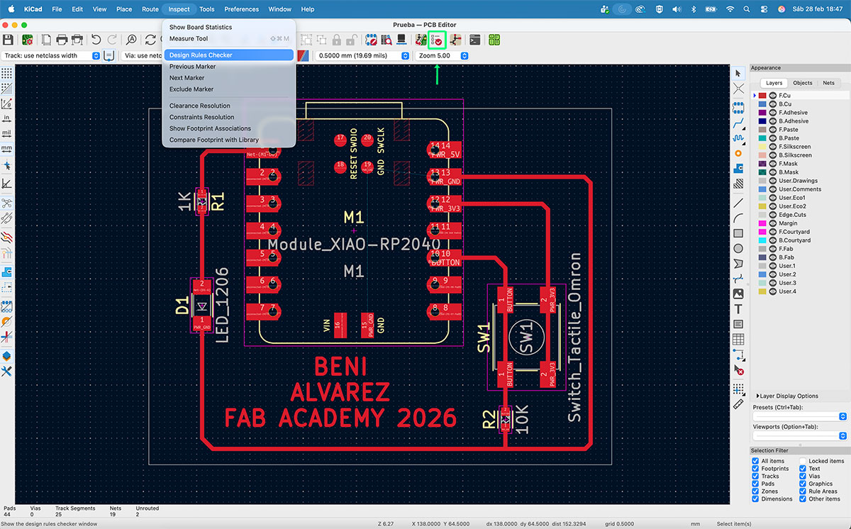
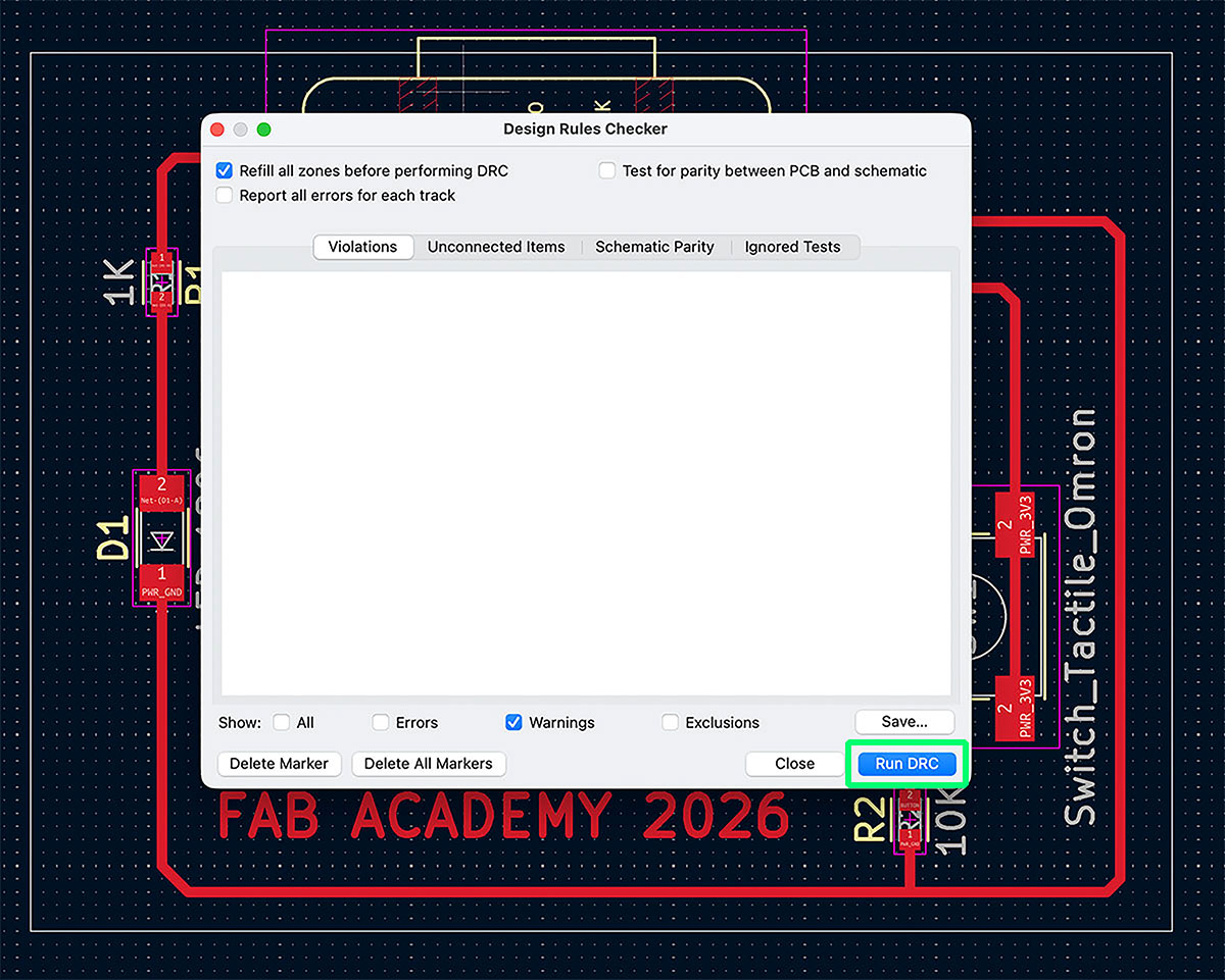
When I was happy with the routing (and with no crossings), I ran a design check: I went to “Inspect” → “Design Rules Checker” (or used the DRC button in the menu) and clicked “Run DRC”.
The result was:
- 2 errors
- 9 warnings
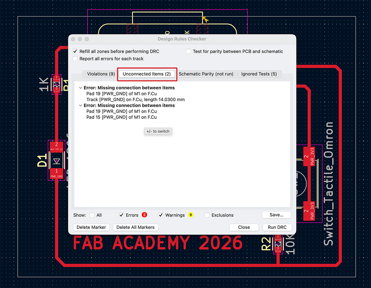
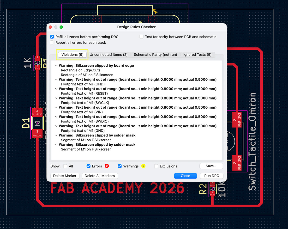
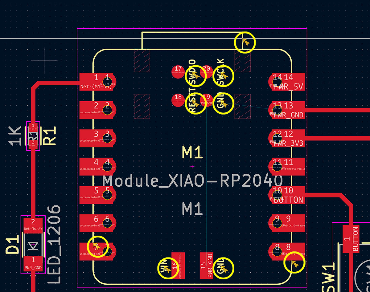
Looking at the 2 errors, I saw they were caused by leaving two extra GND pins on the XIAO unconnected. In my case, this didn’t matter because I wasn’t using those pins, so I noted it and moved on.
Then I reviewed the 9 warnings. Most of them were related to the text/label size on the XIAO footprint, which didn’t affect functionality, so I didn’t treat them as critical.
The remaining warning was more interesting: it indicated that the top edge cut of the board wasn’t outside the XIAO’s USB connector area. In my case, that was intentional and actually helpful, because it improves access to the USB-C port on the XIAO, making it easier to plug and unplug.
Second PCB: XIAO socket version and pin breakout
After finishing the first PCB—and once I had the workflow clear in my head (schematic → update → placement → routing → checks)—I wanted to push it a bit further with a second, more complete version.
This time I decided to use the XIAO socket instead of soldering the module directly. The idea was to keep the microcontroller removable, so I can plug it in and out easily (much more practical if I want to reuse it or iterate on the board later).
Compared to the previous design, I also added a few extra elements:
- An extra button
- An extra LED
- Their corresponding resistors
-
Two PinHeader connectors:
- One with 7 pins (3 + 4)
- One with 6 pins
The goal was simple: break out all XIAO pins to the outside and keep things easy to prototype by providing access to 3.3V, 5V and GND as well—so every pin is ready for sensors, modules or quick experiments without having to improvise wiring.
Once the schematic was complete, I followed the same process as before and moved to the PCB Editor to start the “real” work.
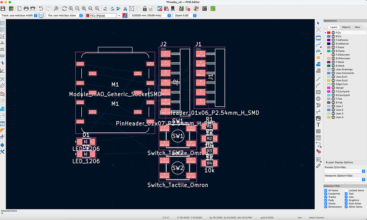
Placement… and the first routing roadblocks
I started by placing the components, trying to keep the layout compact and logical. At first it looked fine, but as soon as I began routing the traces, the problems showed up.
The toughest area was the 7-pin PinHeader on the right side of the XIAO. Crossings kept appearing no matter how I moved traces around. I rotated parts, rerouted, tried different paths… and I kept getting stuck in the same region.
After a few attempts at solving it “cleanly”, I switched to a very common single-layer PCB trick: using 0Ω resistors as jumpers.
Initially, I added:
- 9 × 0Ω resistors to avoid crossings on the 7-pin PinHeader
- And one extra 0Ω resistor for the PinHeader on the left (not visible in the screenshot)
At that moment it wasn’t the prettiest solution, but it was the fastest way to unblock the design and make real progress. I basically used them as small bridges to jump over conflicts without having to redesign the entire board.
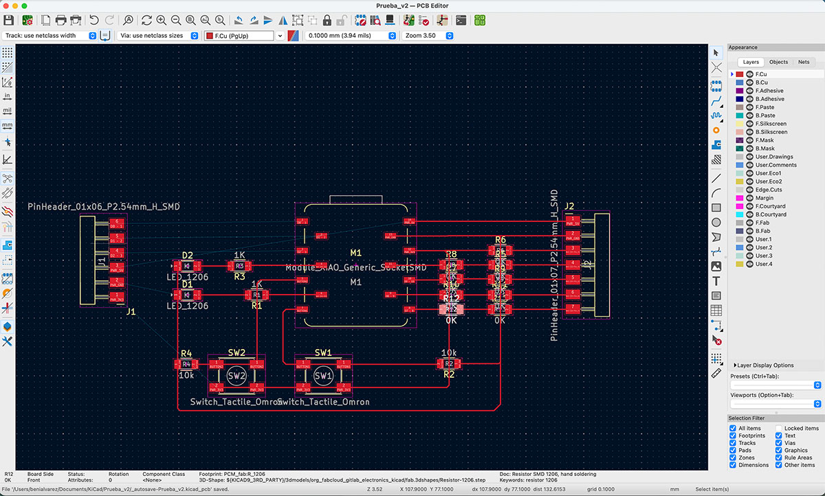
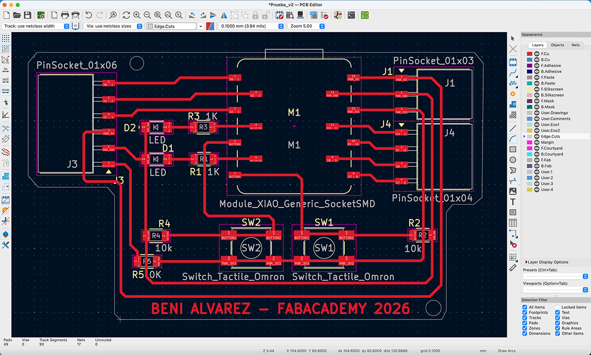
Rethinking the layout and reducing jumpers
Once everything was connected, I took a step back and looked at the PCB… and it didn’t fully convince me. Functionally it worked, but visually it felt too busy, with more jumpers than I wanted.
So I paused and rethought the routing with a calmer approach. I slightly reorganized the placement and focused on how to route the power lines more intelligently. That’s when I realized I could run the 5V and GND traces under the PinHeaders, using the space much more efficiently and freeing up the crowded area.
That small change made a huge difference.
With the improved routing, I managed to remove 5 of the 0Ω resistors I originally added. The board immediately looked cleaner and more coherent, while still keeping all connections conflict-free.
Final adjustment and complete removal of jumpers
Just when I thought the design was basically finished, I decided to take one more careful look. By this point I had already learned something important: there is almost always a slightly better solution if you give yourself the time to find it.
While reviewing the traces, I focused on the 3V3 line coming from the switches and going to the corresponding XIAO pin. Up until that moment, I was routing it on the top side, which forced me to keep a few crossings — and therefore several 0Ω resistors acting as jumpers.
Then a simple idea came to mind: what if I route that 3V3 trace under the PinSockets on the right, just like I had already done with 5V and GND?
I tried rerouting that section underneath the connectors… and it worked.
By reorganizing that path, I managed to eliminate the remaining crossings and, as a direct consequence, I was able to remove the last 4 × 0Ω resistors that were still acting as bridges.
The board was finally free of jumpers.
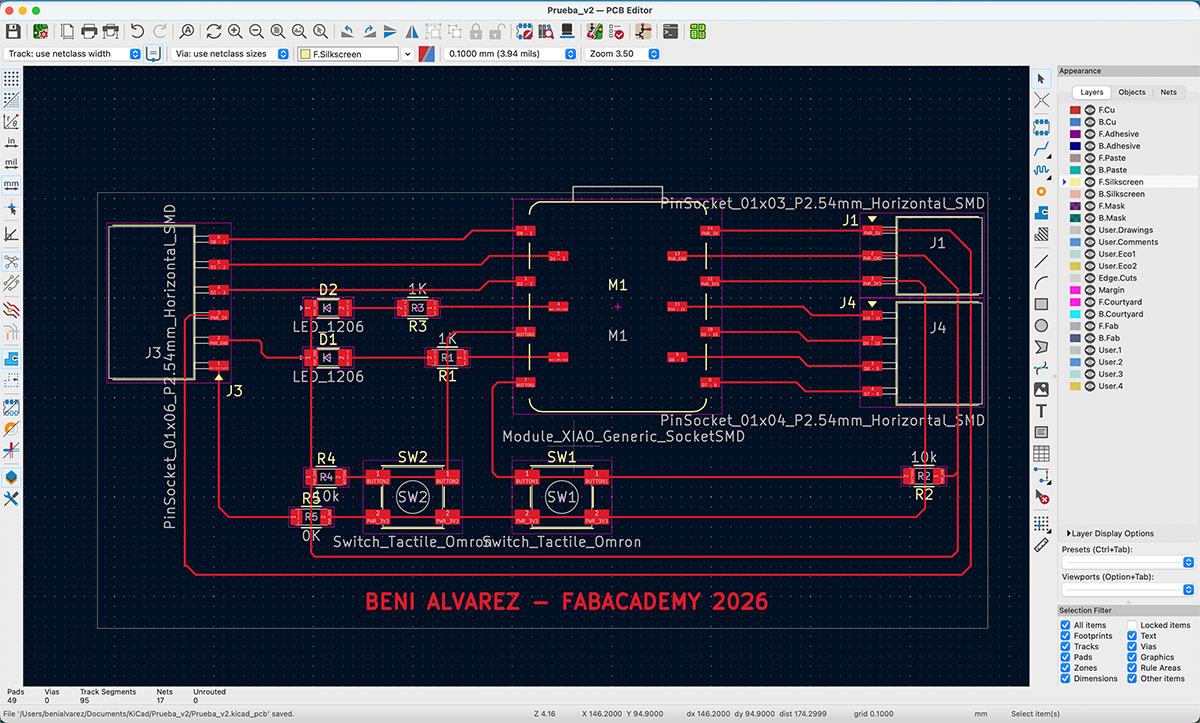
Local instructor review
After the weekly review with the local instructors every Monday, they've pointed out a couple of errors/improvements:
- The traces aren't 0.4mm thick, so I need to correct that.
- Try to make the PCB smaller.
- The cutting line shouldn't be a basic rectangle.
- Add holes.
So, let's get to it (V 2.4)
This is the result.
Interactive HTML BOM: Prueba_v2.4.html BOM
Final reflection
If there is something this second PCB taught me, it’s that board design is not a linear process.
By repeatedly doing and redoing parts of the layout every time I spotted a possible improvement, I realized that this is really about investing time, testing alternatives, and gradually understanding the real possibilities you have when simplifying a circuit.
In this case — and being honest about my current level — these circuits are quite basic. But even in something simple like this, I clearly experienced how many changes can happen between the initial idea and the final result.
Each iteration made me notice things that I simply couldn’t see in the first attempt.
Will this last version be the definitive one?
I DON'T THINK SO!.
And honestly, that’s probably the most interesting part of the whole process.
Carboard first model of Final Project
Although it has nothing to do with this week's theme (electronic design), this week I made a first cardboard model in order to start analyzing possible measurements, problems and solutions when carrying out my final project.
Final project development - Week06 sectionOriginal code files for this documentation
Files for download
- PCB V1 KiCad files (PCB_v1.zip) ZIP · 20 Kb
- PCB V2.4 KiCad files (PCB_v2.zip) ZIP · 31 Kb
Credits
Thanks to local instructors Nuria, Pablo and Adrián for their explanations, and especially thanks to my colleague Oscar Cela for his master classes in basic electronics and for helping me understand some things.
All texts were written in Spanish and translated into English using Google Translate and ChatGPT.