Week 8: Electronics Production
The focus of this week was producing a functional printed circuit board (PCB) using digital fabrication tools. The process involved generating fabrication files from a PCB design, milling the board using a PCB milling machine, soldering electronic components onto the board, and finally programming and testing the board to ensure it functions correctly.
By the end of the week, the goal was to have a fully assembled and operational PCB.
The workflow for this week included:
This week was guided by Saheen, Sibin, and Revisankar.
Group Assignment Insights
Click to view details on our Group Assignment page.
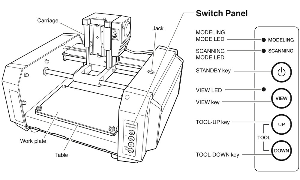
The Roland Modela MDX-20 is a compact 3-axis (X, Y, Z) desktop milling machine used for precision fabrication tasks such as PCB prototyping. It is widely used in educational and small-scale production environments due to its reliability and fine control over toolpaths.
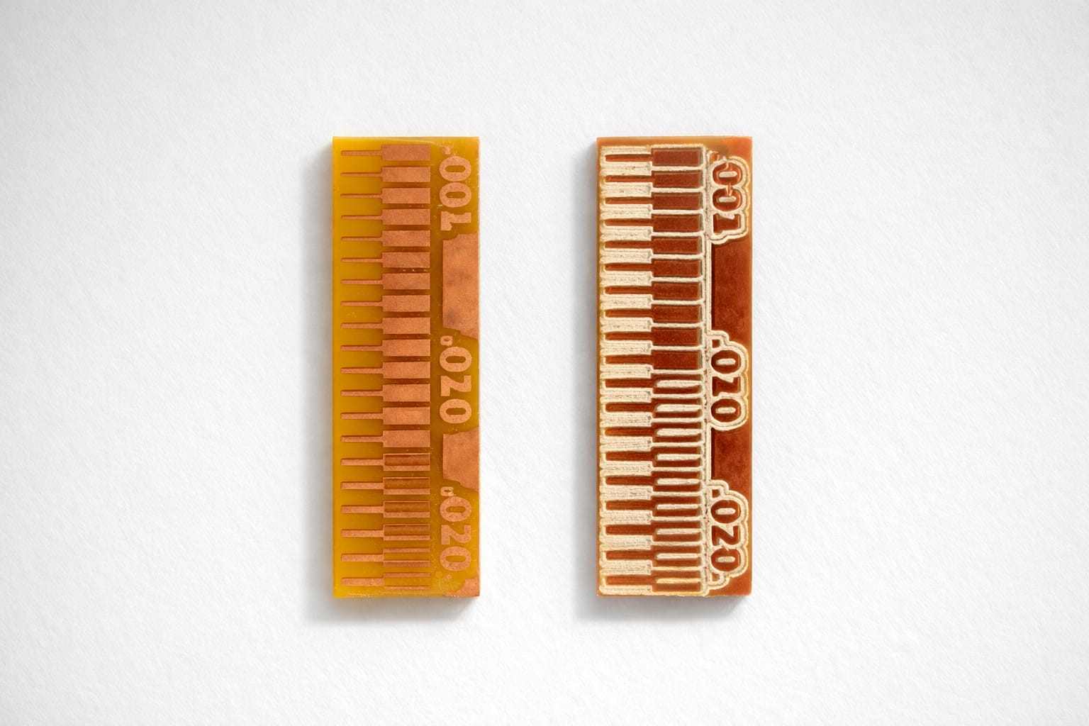
The first test piece was traced using a 0.4 mm flat end mill, while the one on the right was done using a 0.2 mm V-bit. For the individual assignment, a V-bit is being used.
Observations and Constraints
Smaller spacing increases risk of:
These values depend on:
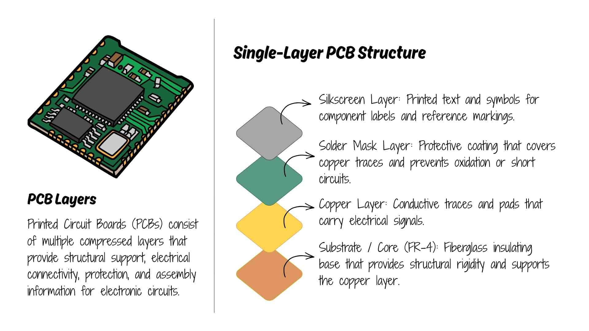
Introduction to PCBs
The week began with a lecture presentation by Sibin, introducing the structure and components of a printed circuit board (PCB). This provided the foundational understanding required before moving into fabrication.
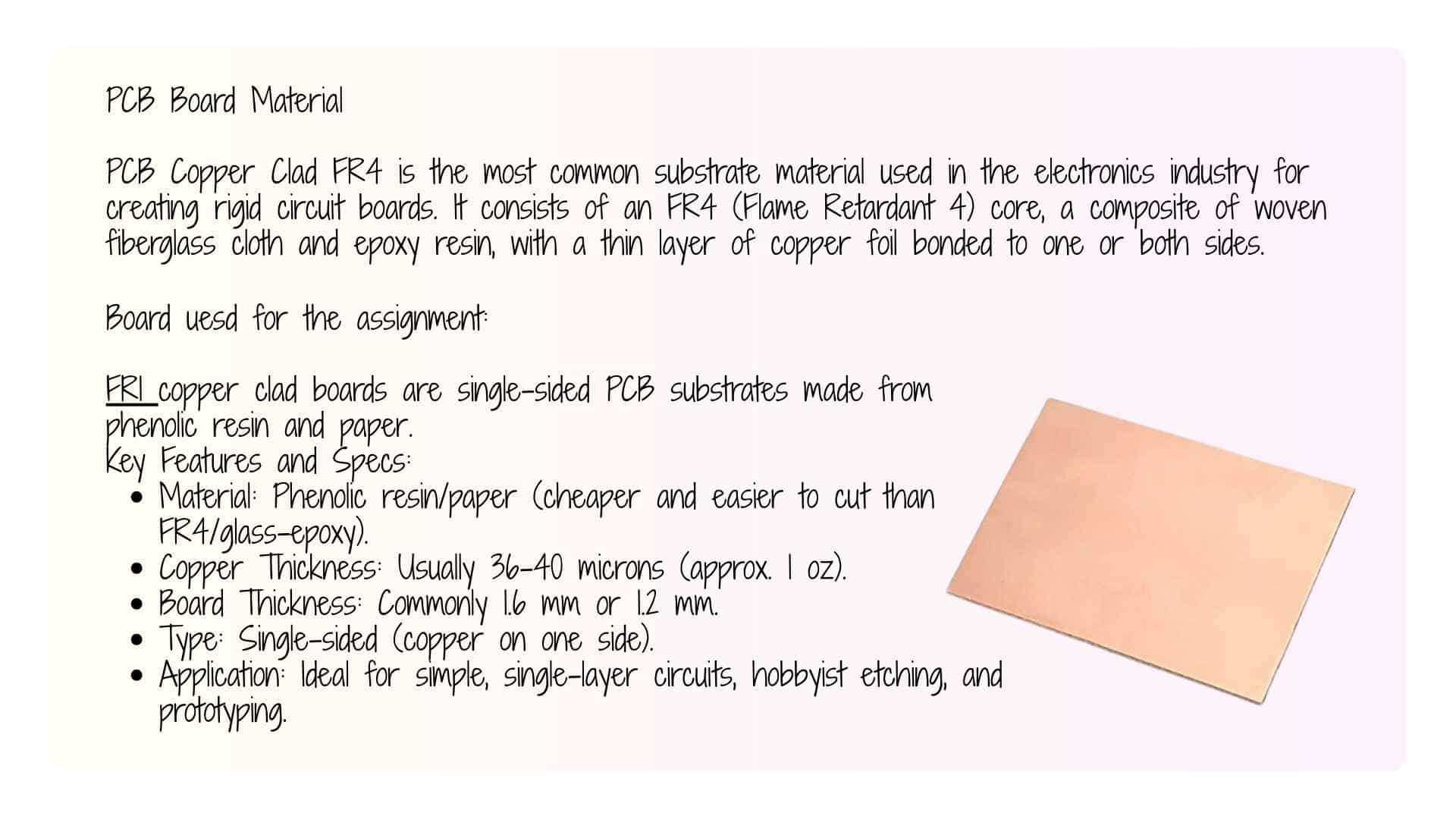
A PCB mechanically supports and electrically connects electronic components through conductive pathways etched from copper sheets laminated onto an insulating substrate.
Preparing Fabrication Files in KiCad
After the introduction, the focus shifted to preparing fabrication files from KiCad.
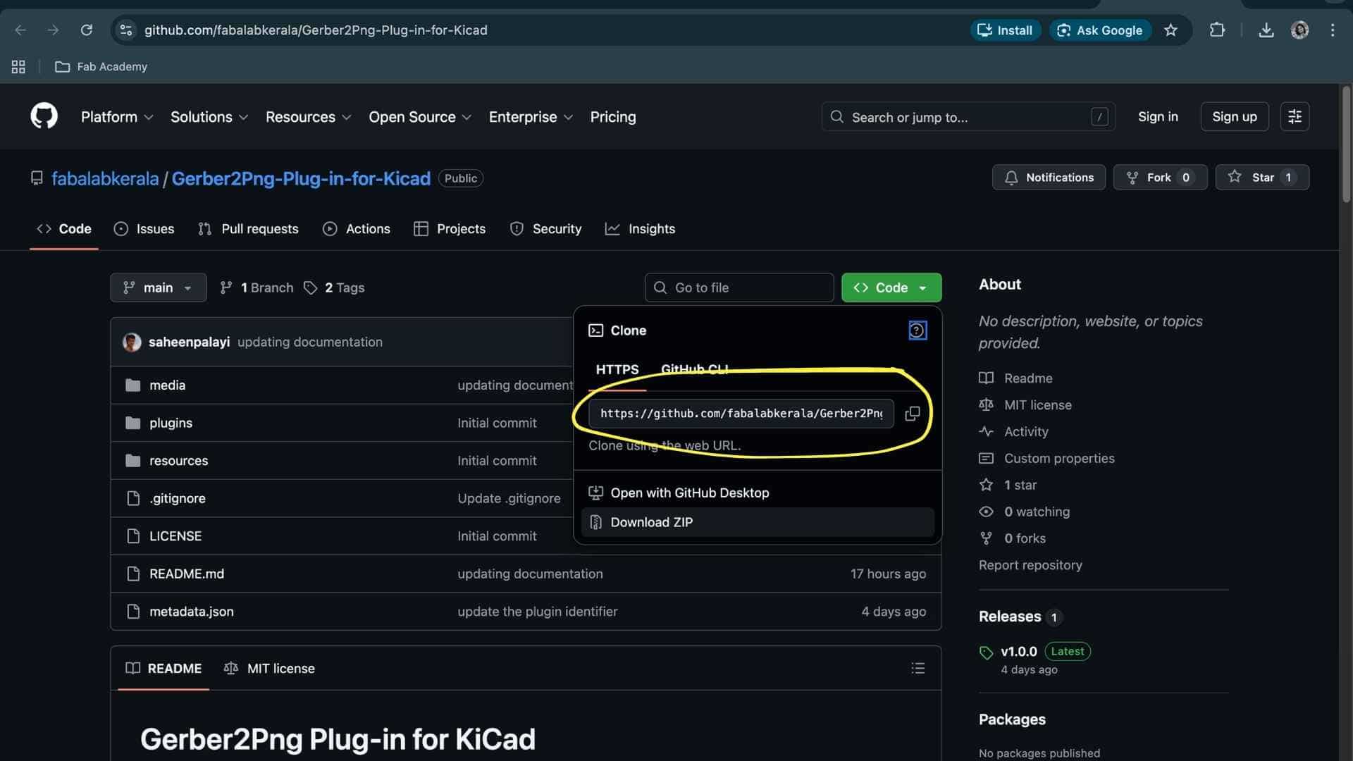
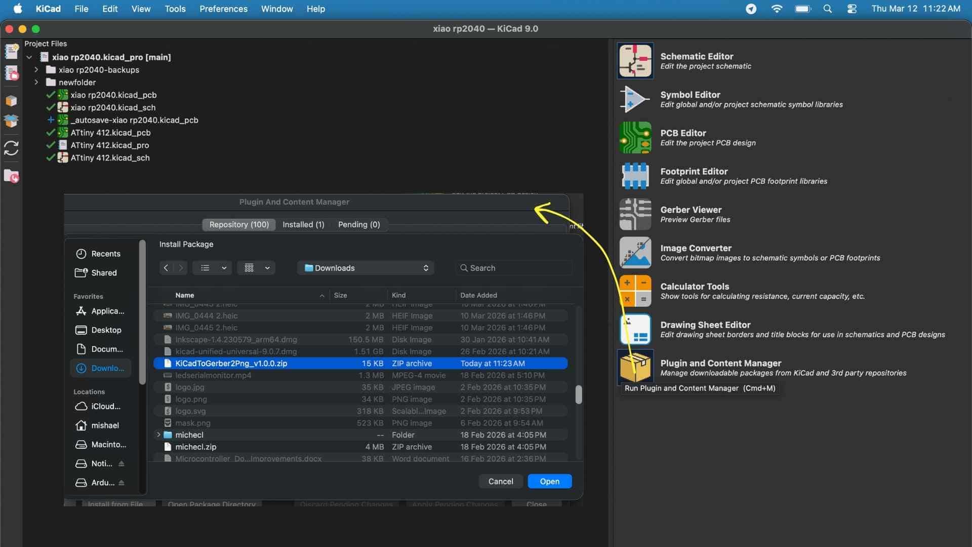
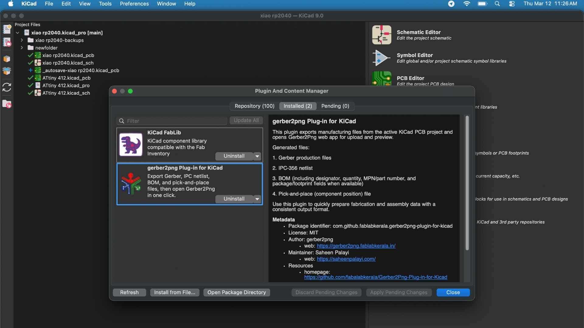
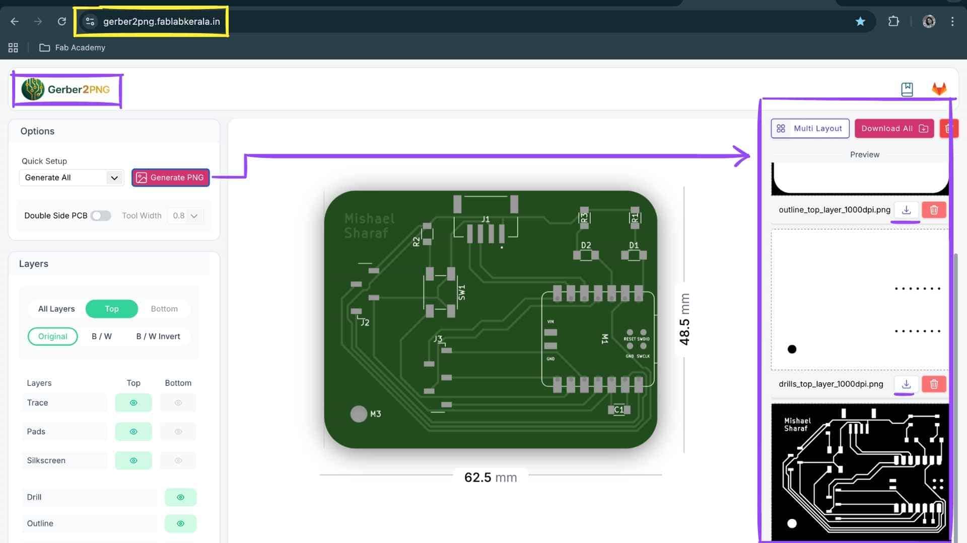
gerber2png Plugin
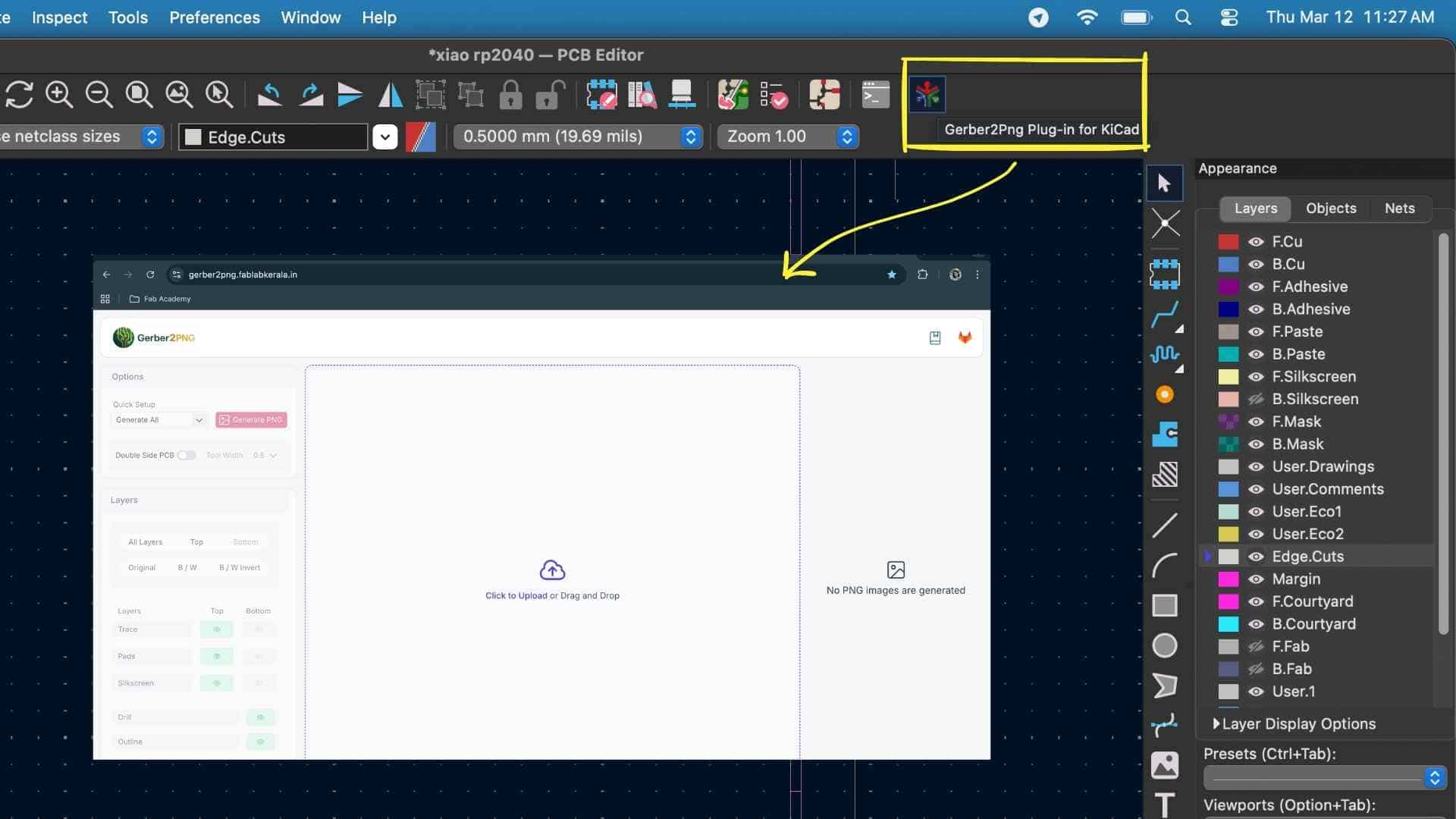
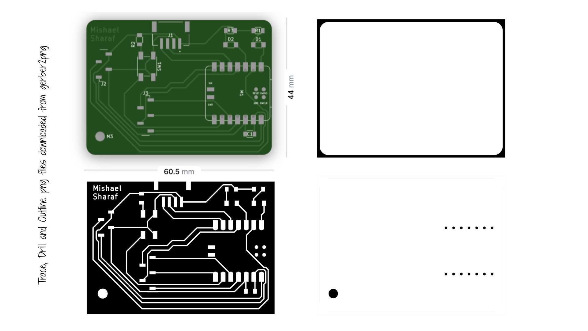
The Gerber2PNG plugin was installed in KiCad to convert PCB fabrication files into PNG images suitable for the PCB milling workflow used in the lab.
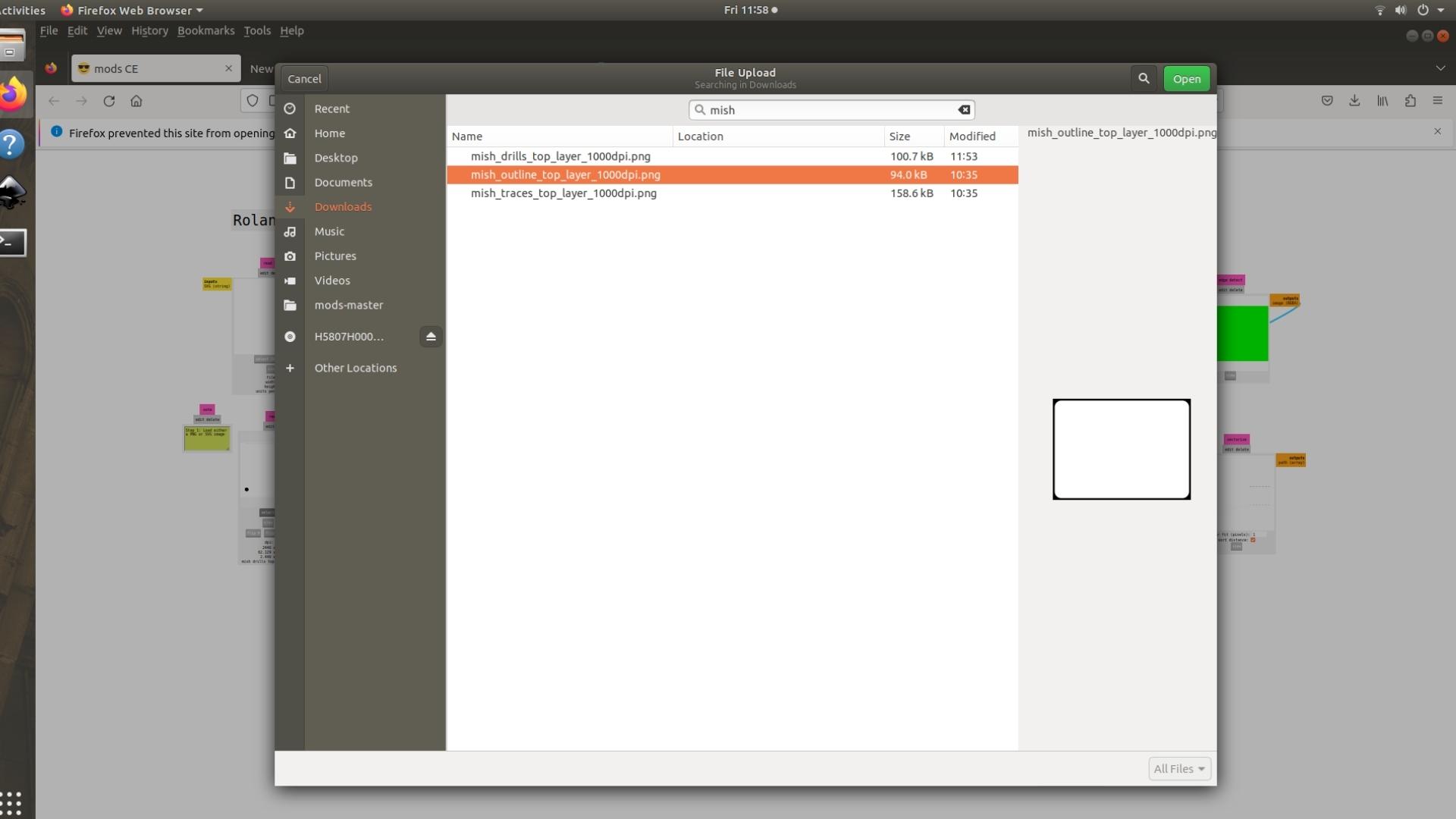
Using this plugin, the following files were generated:
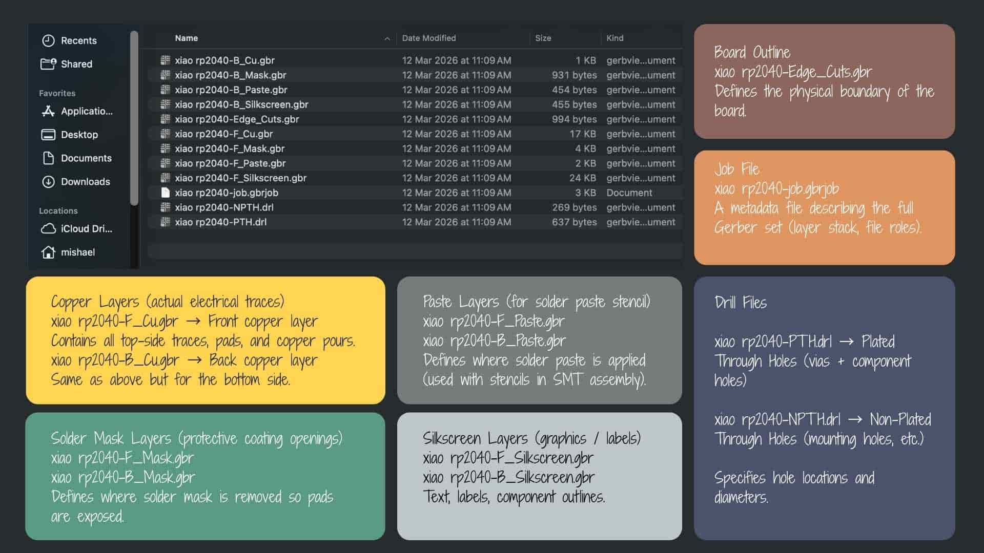
The gerber2png website allows you to download the following png files:
These files are later used to generate toolpaths for PCB milling.
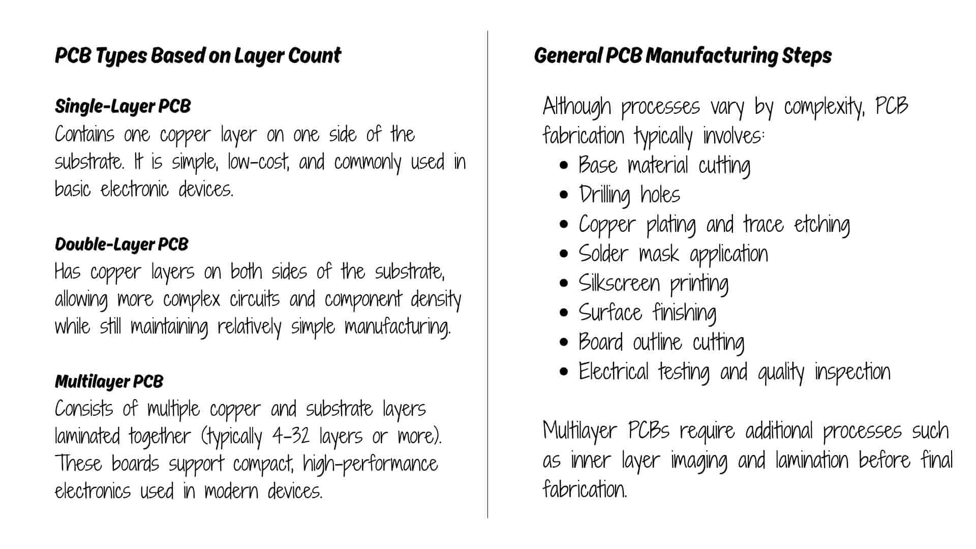
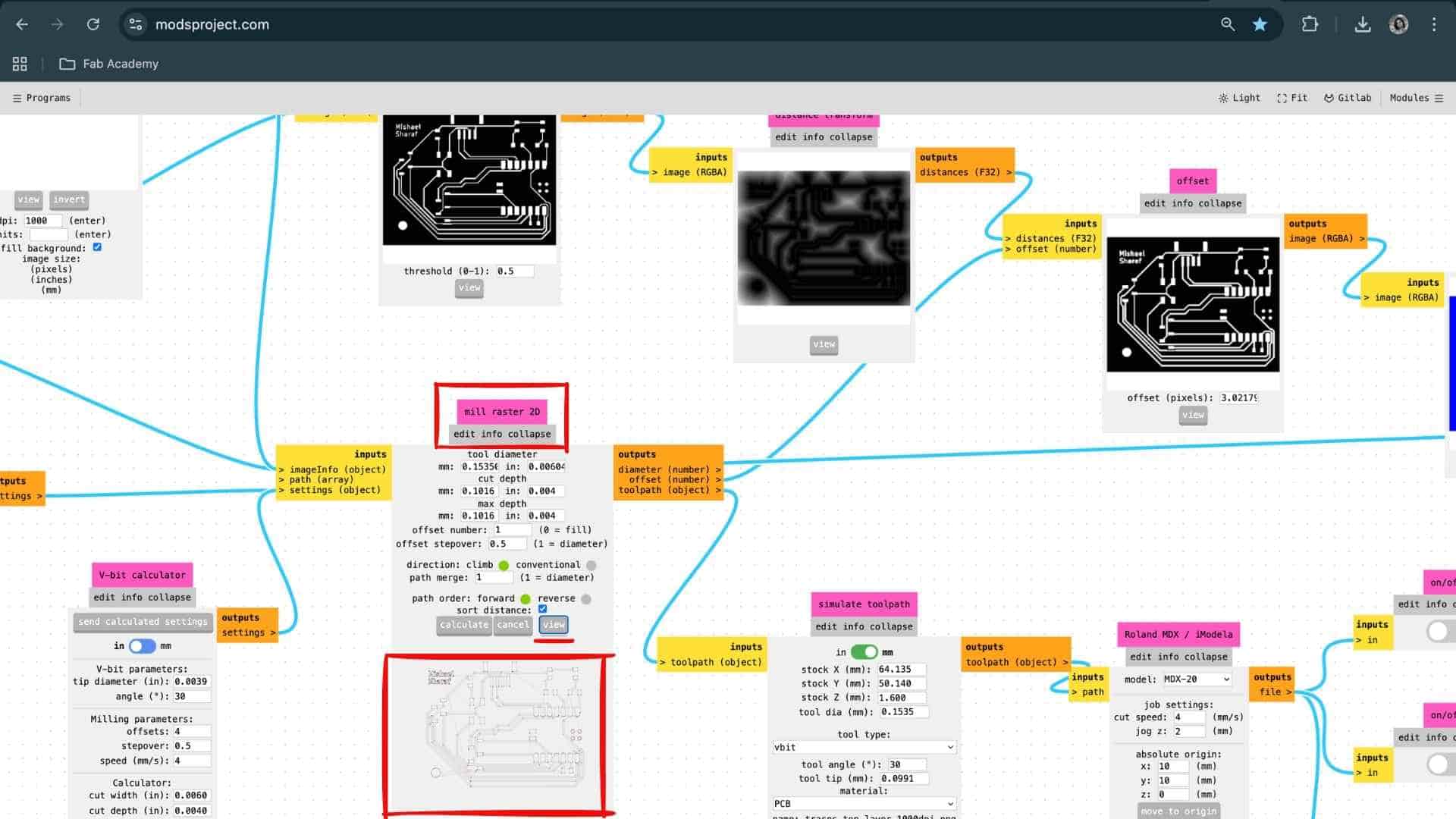
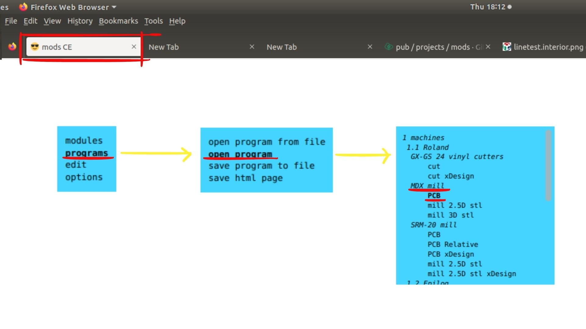
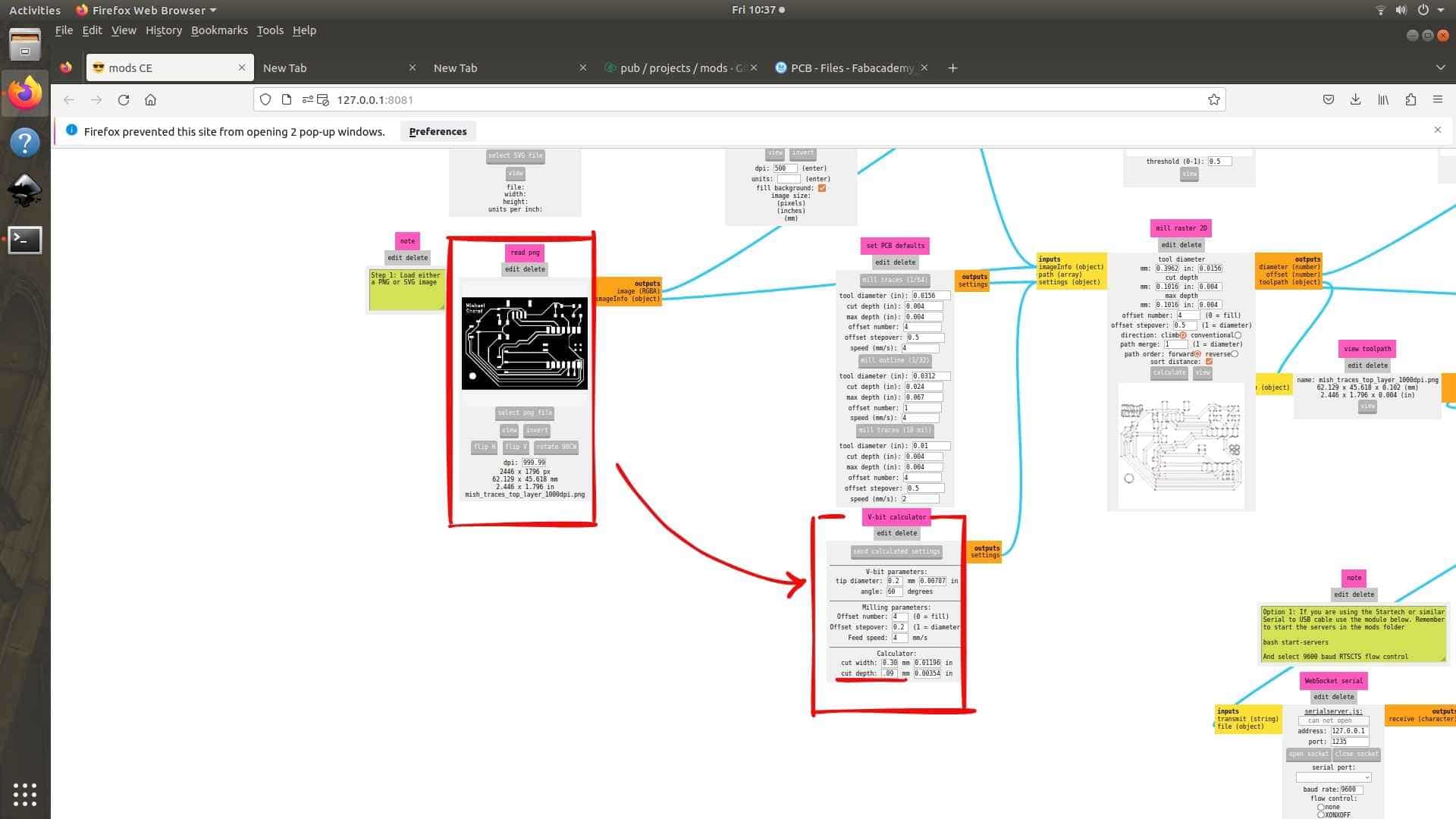
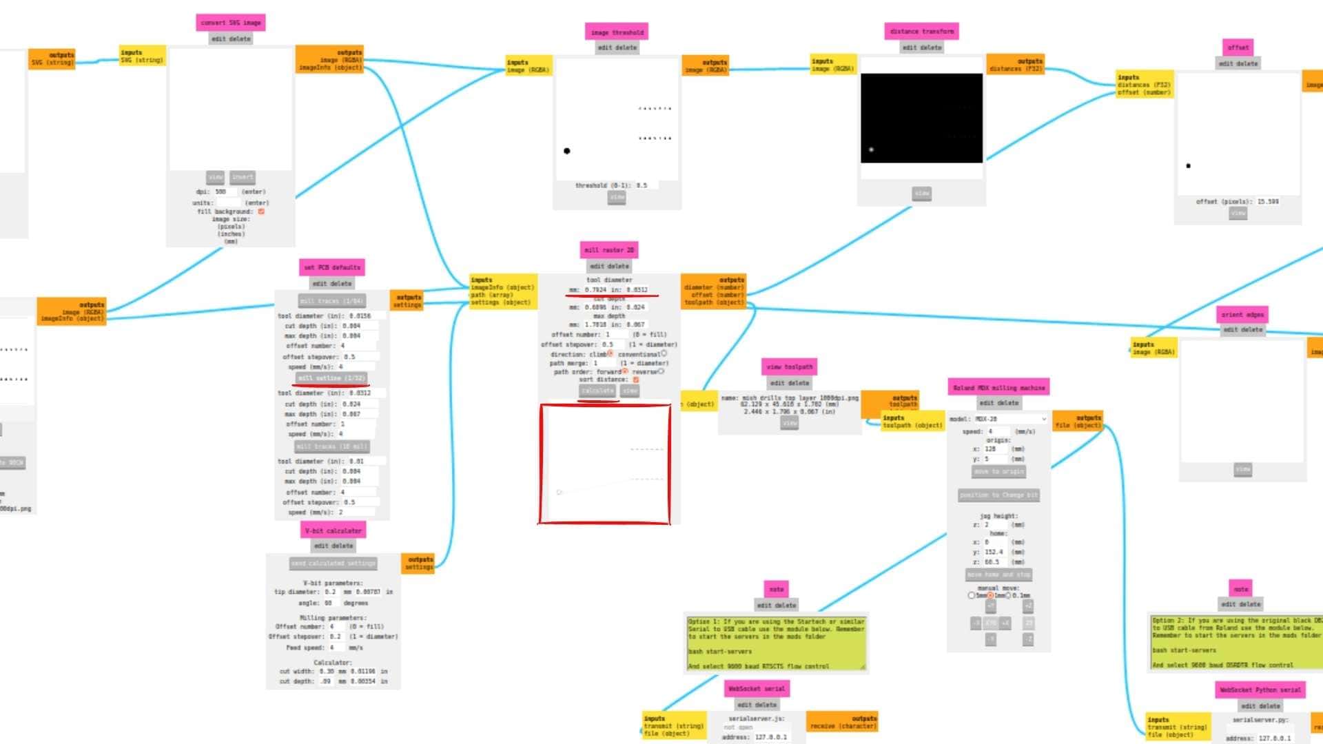
Generating Toolpaths with Mods Project
After preparing the PCB fabrication files, the next step was to generate toolpaths for milling the board. For this workflow, the Mods Project was used.
Mods is a modular, browser-based software environment developed at MIT. It is commonly used in Fab Labs to convert PCB design files into machine instructions (G-code or RML) that can be executed by desktop PCB milling machines.
In this case, Mods was used to convert the exported PNG trace and outline files into toolpaths for the milling machine.
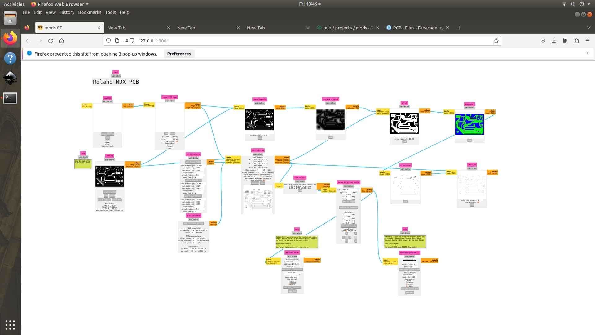
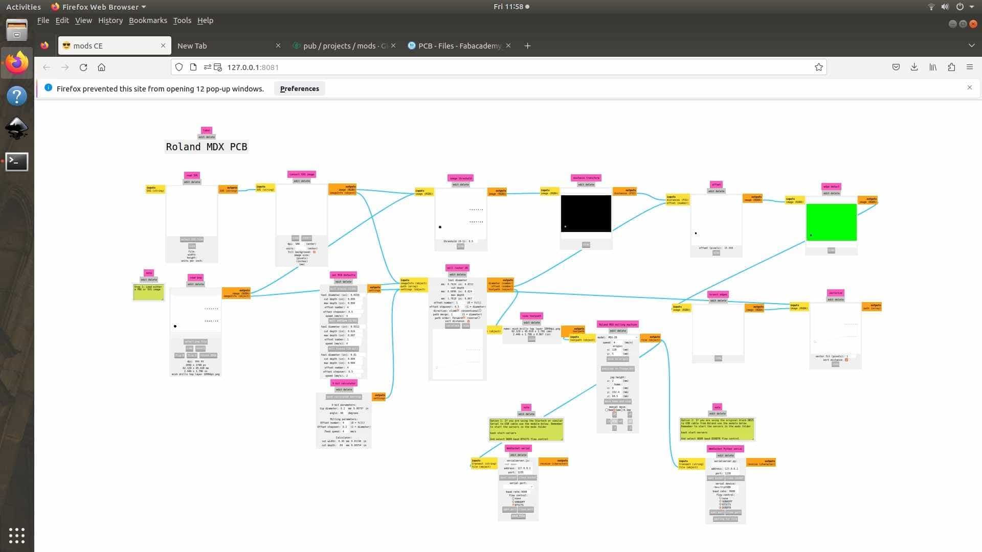
Mods can be accessed directly through a web browser. After opening the Mods interface, the PCB milling program is loaded.
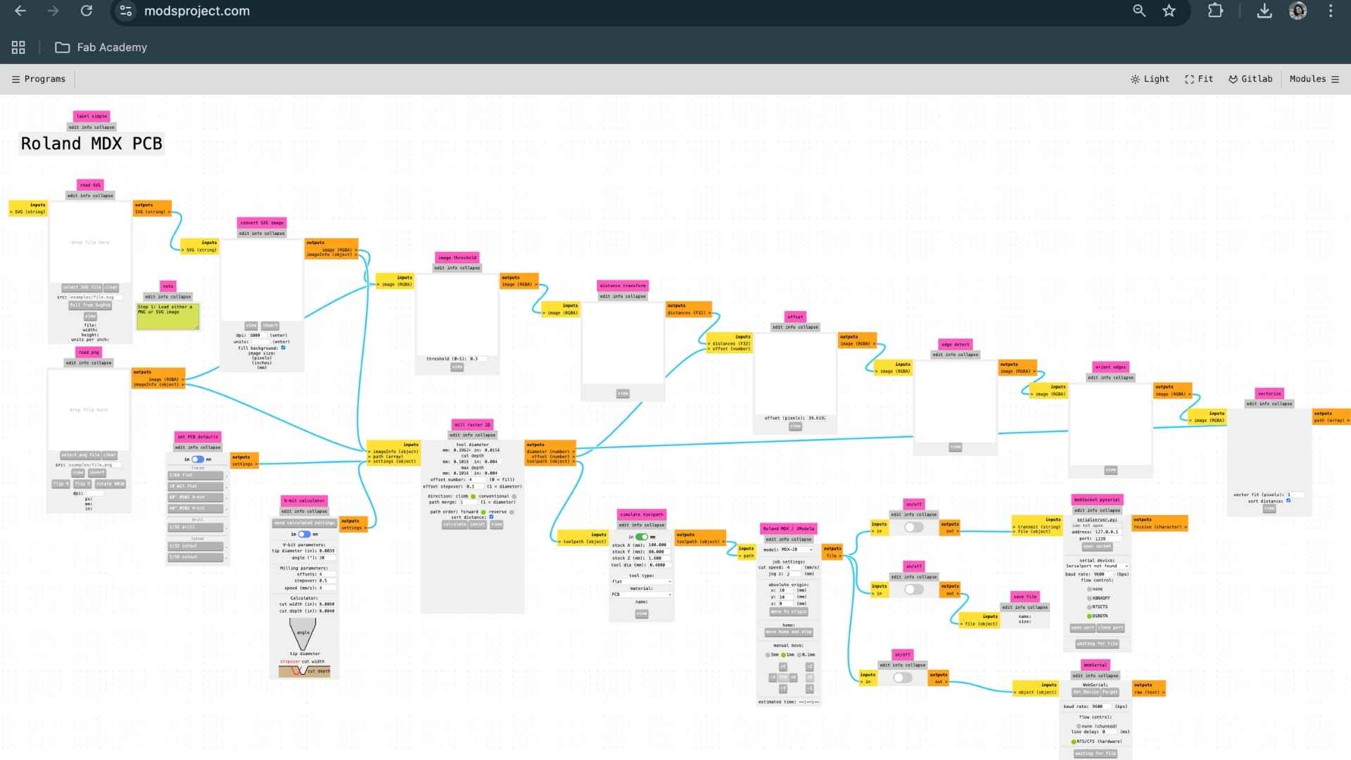
The loaded program usually contains the following modules:
PCB Production (Milling)
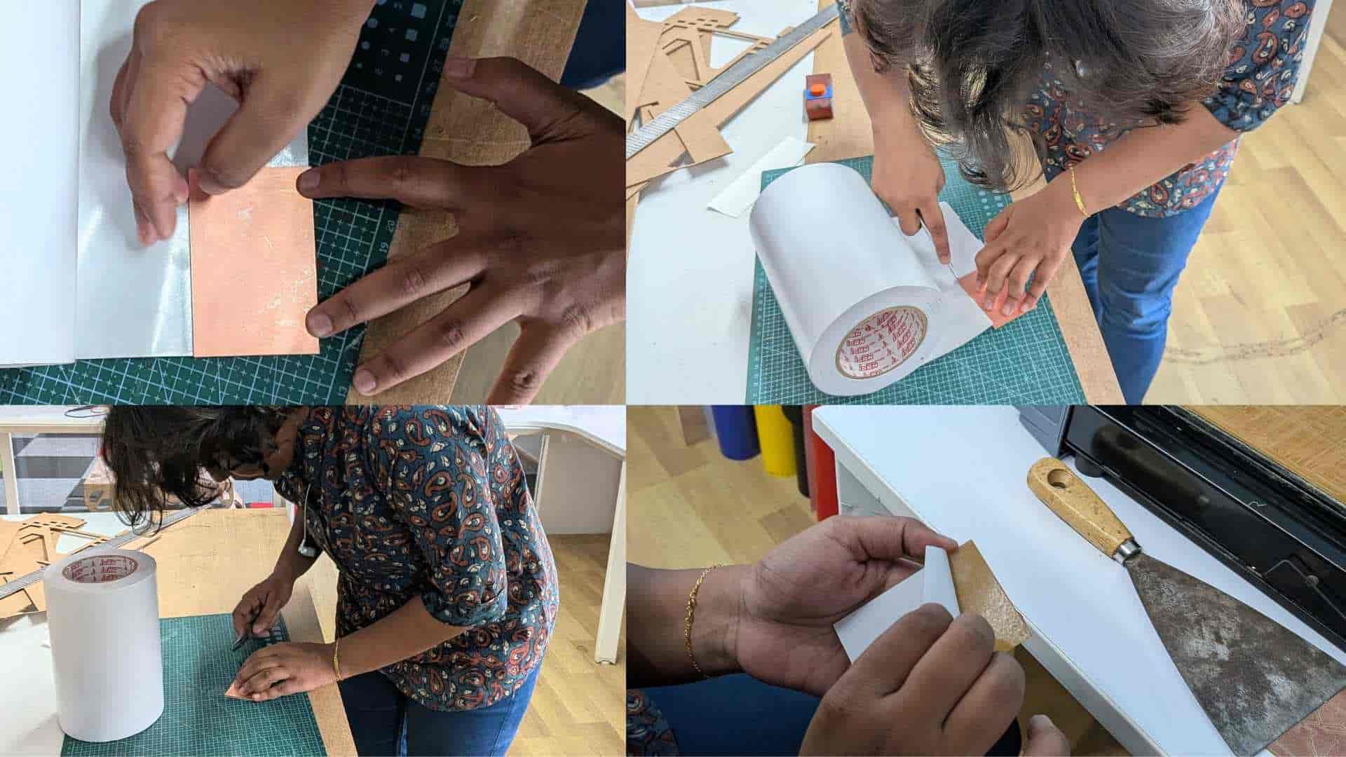
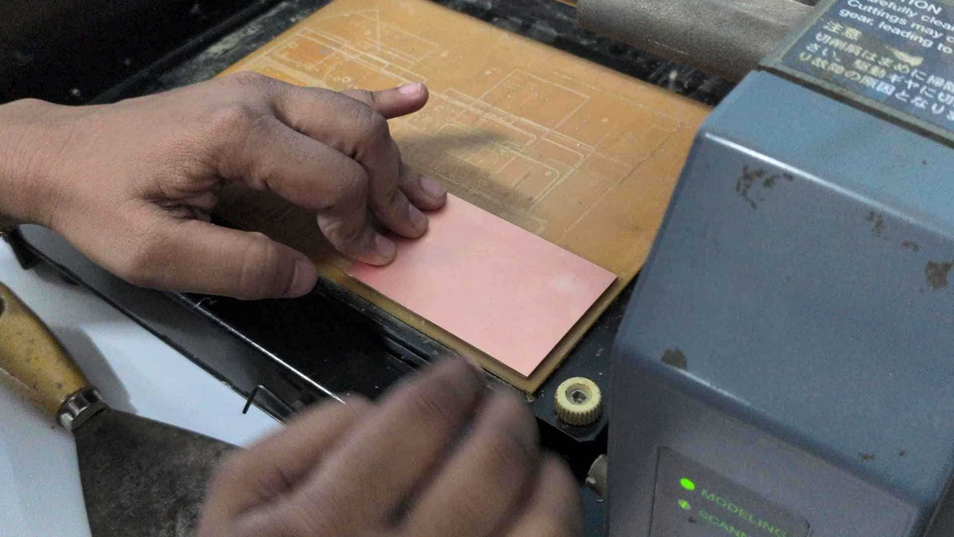
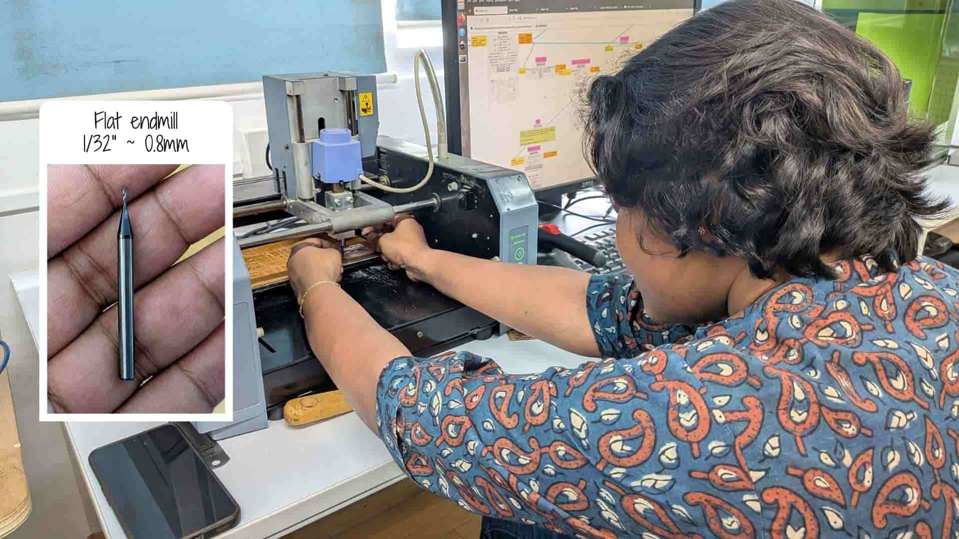
The PCB blank was first fixed onto the bed of the Roland Modela MDX-20 using double-sided tape to ensure it remained stable during milling.
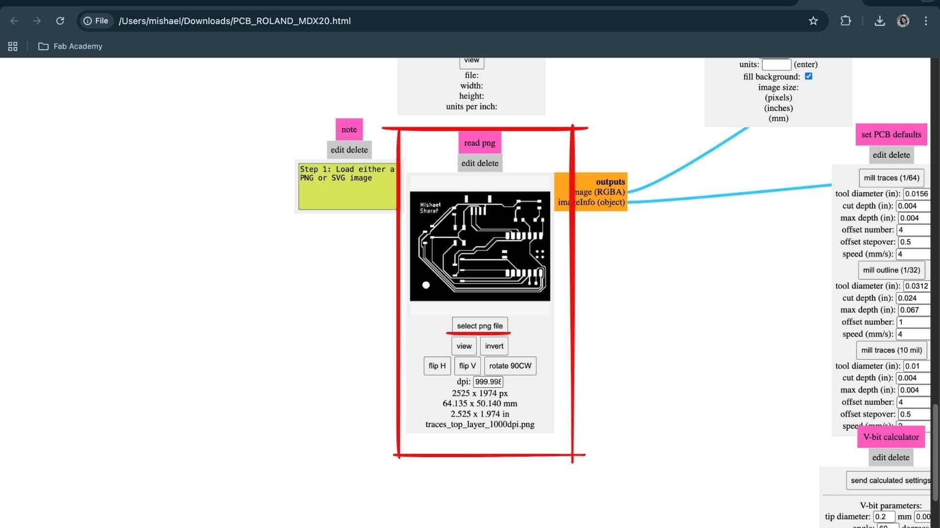
Next, the offline version of Mods Project used in the lab was opened and the trace PNG generated from Gerber2PNG was loaded.
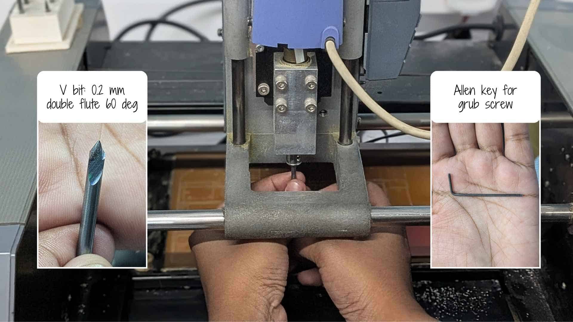
Using an Allen key, the grub screw was loosened and the V-bit was inserted. The machine was then returned to the origin position. The bit was gently lowered until it touched the PCB surface, after which the grub screw was tightened. This procedure set the Z-axis reference for milling the traces.
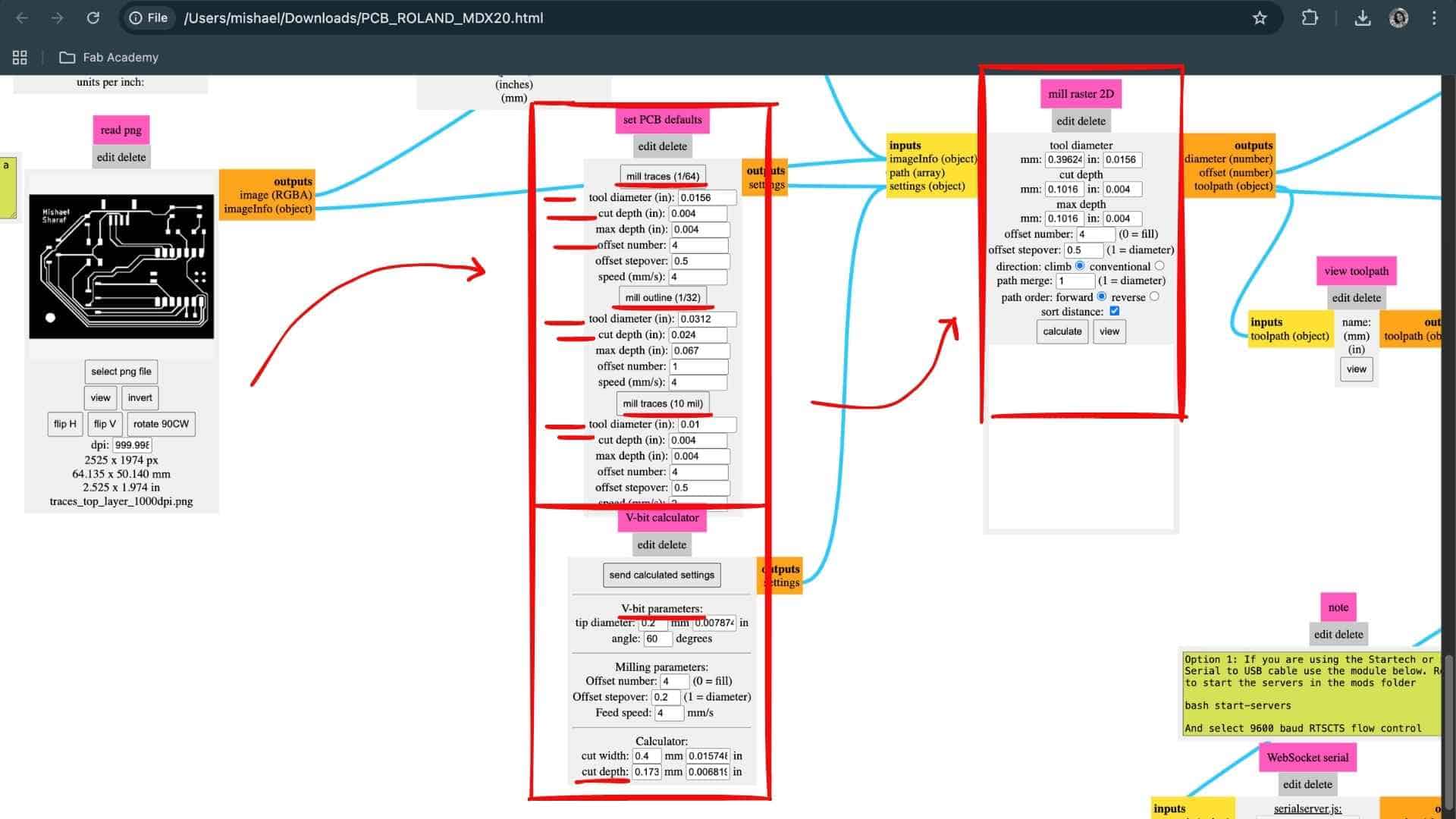
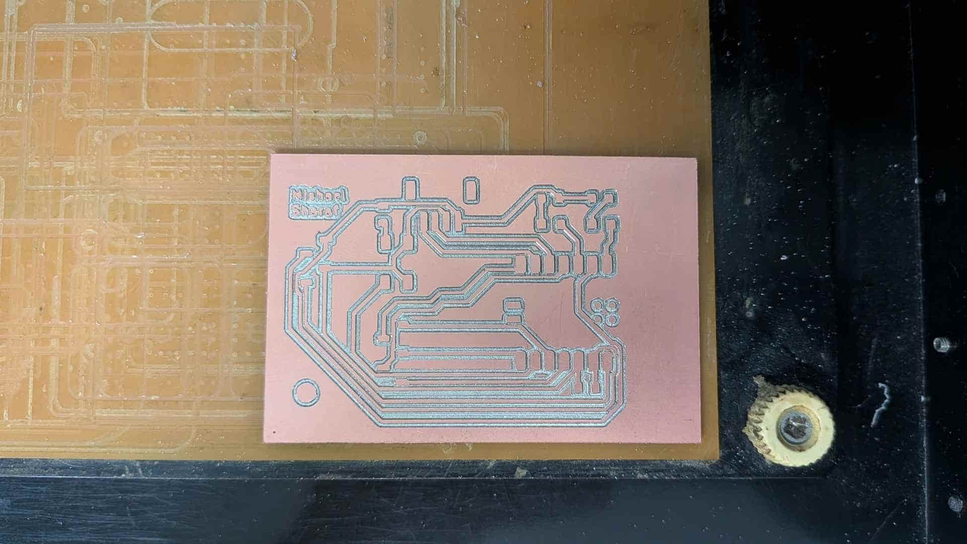
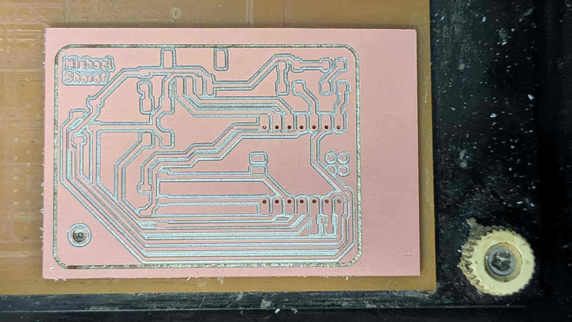
Milling Trace -Top Layer
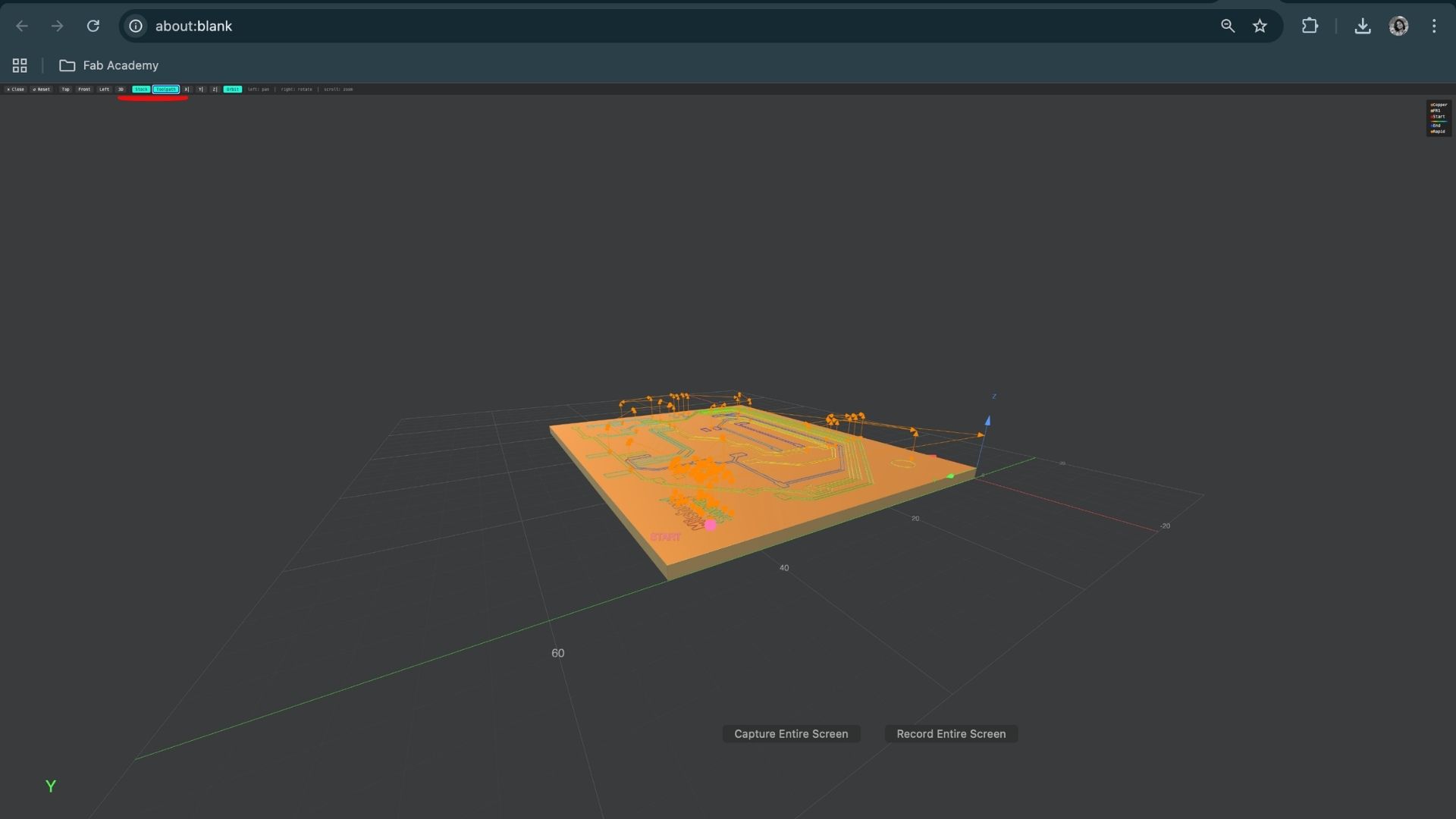
With the V-bit selected, the milling parameters were adjusted in Mods Project. The cut depth was set to 0.09 mm, and the toolpath was generated by clicking Calculate.
After verifying the toolpath preview, the job was started by clicking Send File, which began milling the PCB traces on the Roland Modela MDX-20.


Milling Drills -Top Layer
Issue with Drill Holes in Mods
While generating the toolpaths in Mods Project, an issue appeared when loading the drill PNG file.
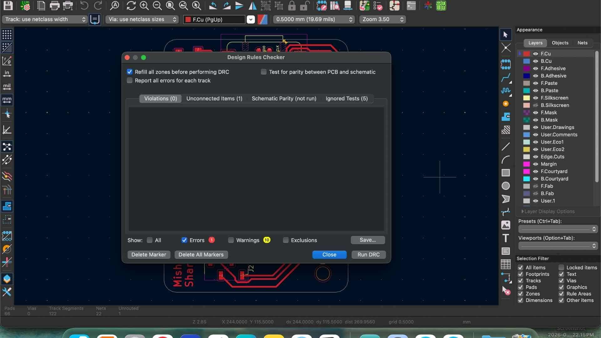
After loading the traces PNG, drill PNG, and outline PNG, the toolpaths were calculated using the Calculate function in Mods. The traces and outline appeared correctly in the calculated preview. However, when the drill PNG was loaded, the pin holes for the microcontroller (XIAO RP2040) were not visible in the calculated toolpath preview.
This indicated that the milling machine would not recognize or mill those holes.
Cause of the Issue
The issue originated from a mismatch introduced during the Gerber-to-PNG conversion process.
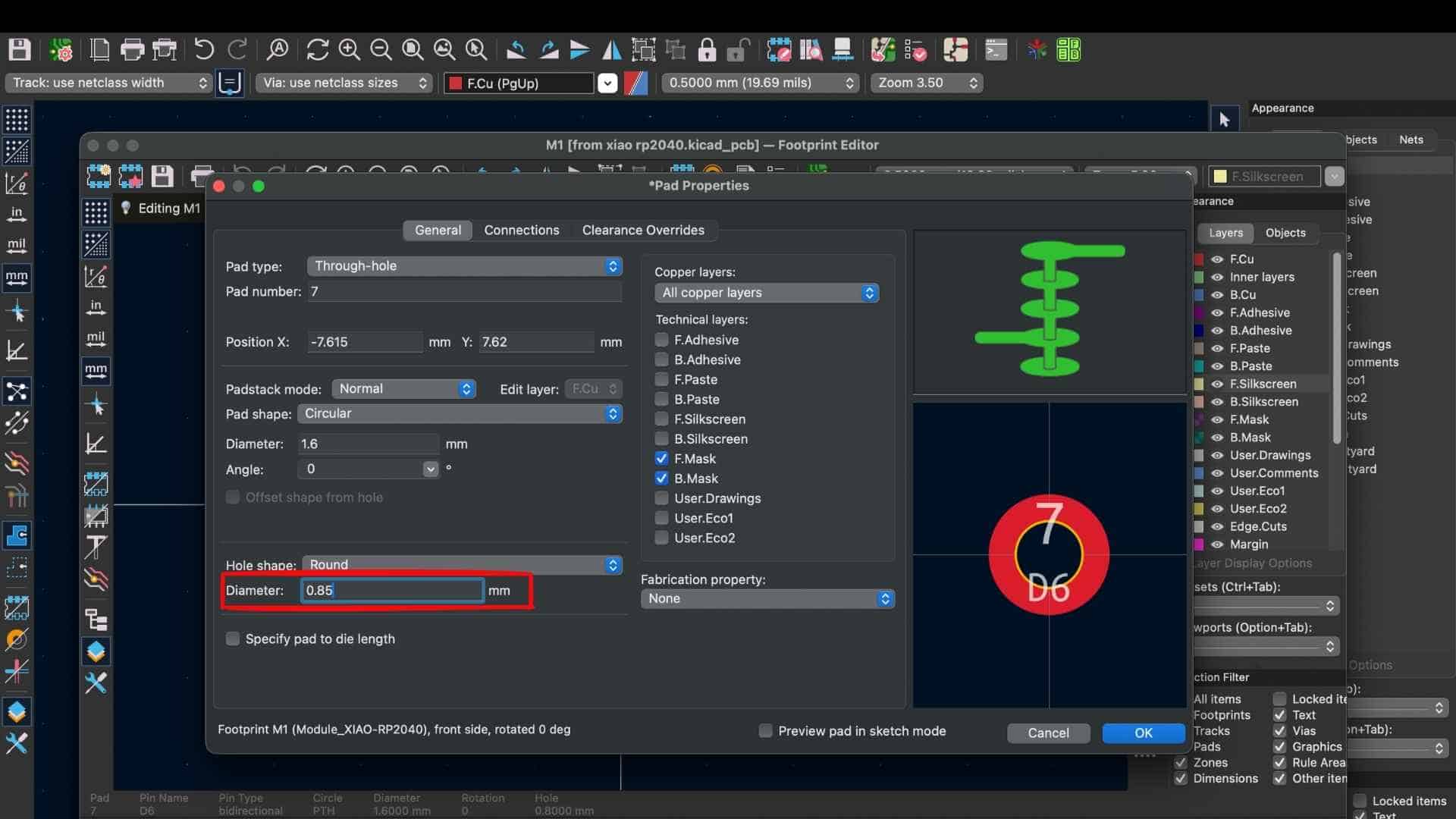
In the KiCad footprint for the Seeed Studio XIAO RP2040, the pin hole diameter was defined as 0.8 mm, which exactly matched the diameter of the drill bit used for milling. Due to a known bug in the Gerber2PNG plugin, a slight tolerance error was introduced during export.
Because the hole diameter and tool diameter were identical, this small deviation prevented Mods from correctly recognizing the hole geometry during toolpath generation. Consequently, the holes were omitted from the preview.
Solution
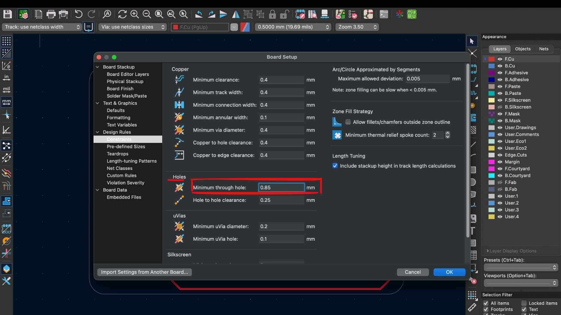
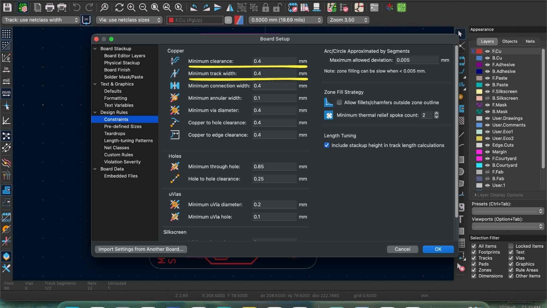
In KiCad PCB Editor, the minimum through-hole constraint was first changed from 0.8 mm to 0.85 mm.
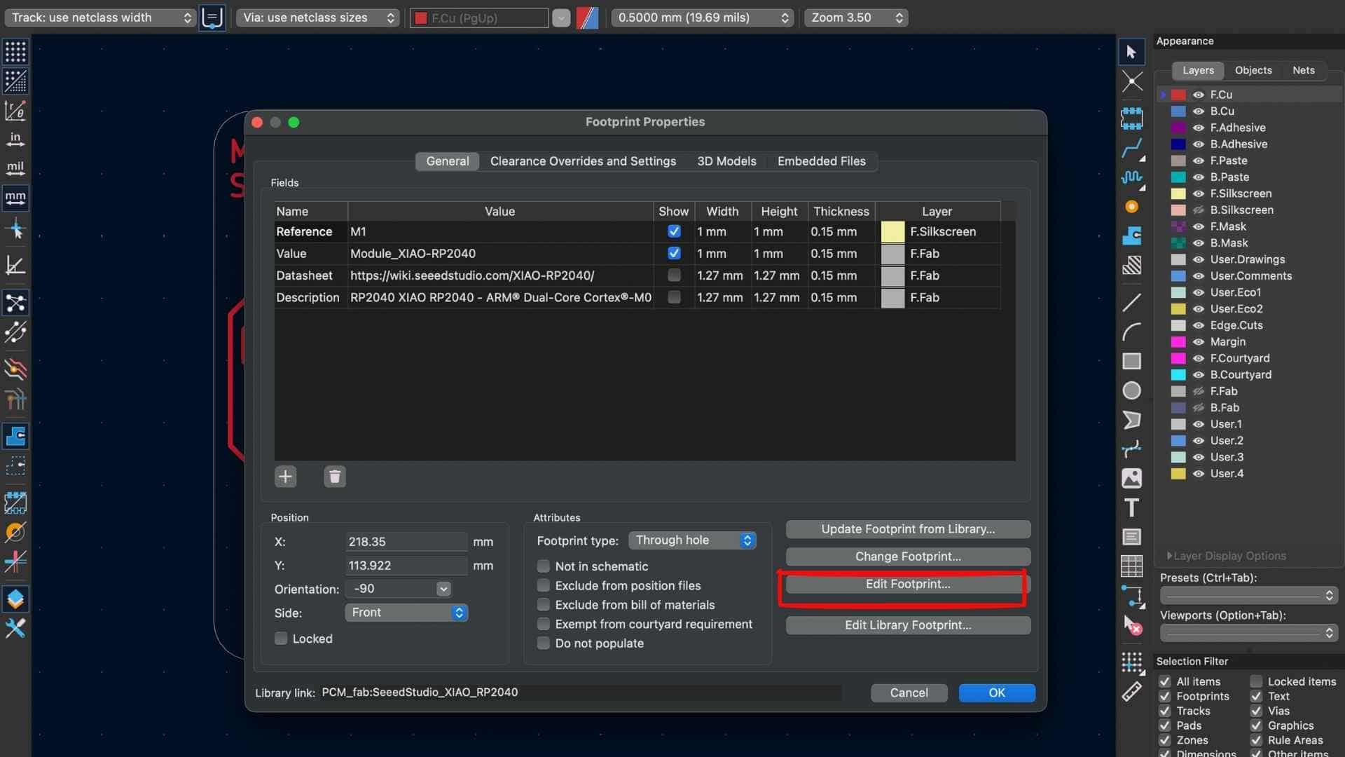
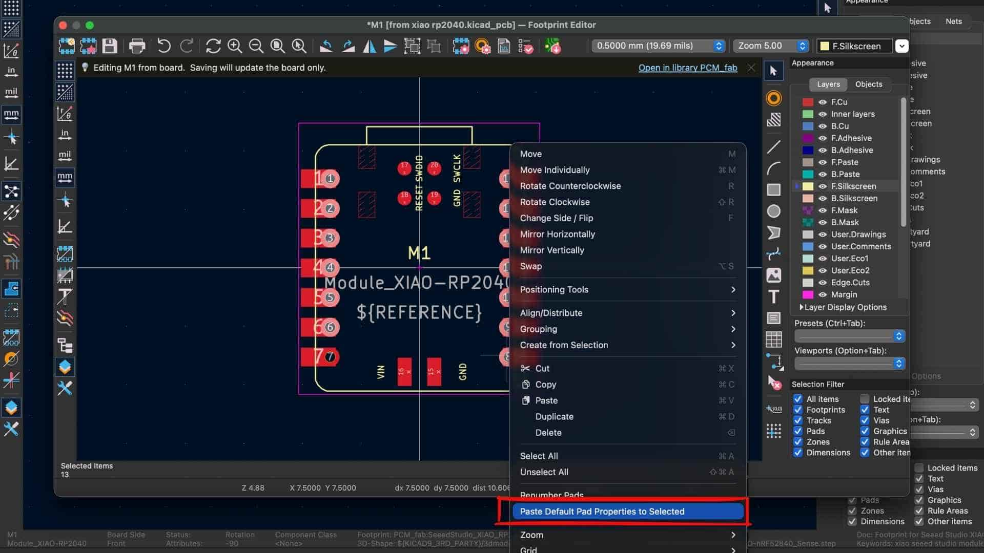
To further resolve this issue, the footprint in KiCad had to be modified. Steps taken:
Result

After increasing the drill hole diameter and regenerating the PNG files, the holes appeared correctly in the toolpath preview inside Mods. This confirmed that the milling machine would correctly recognize and mill the holes during fabrication.
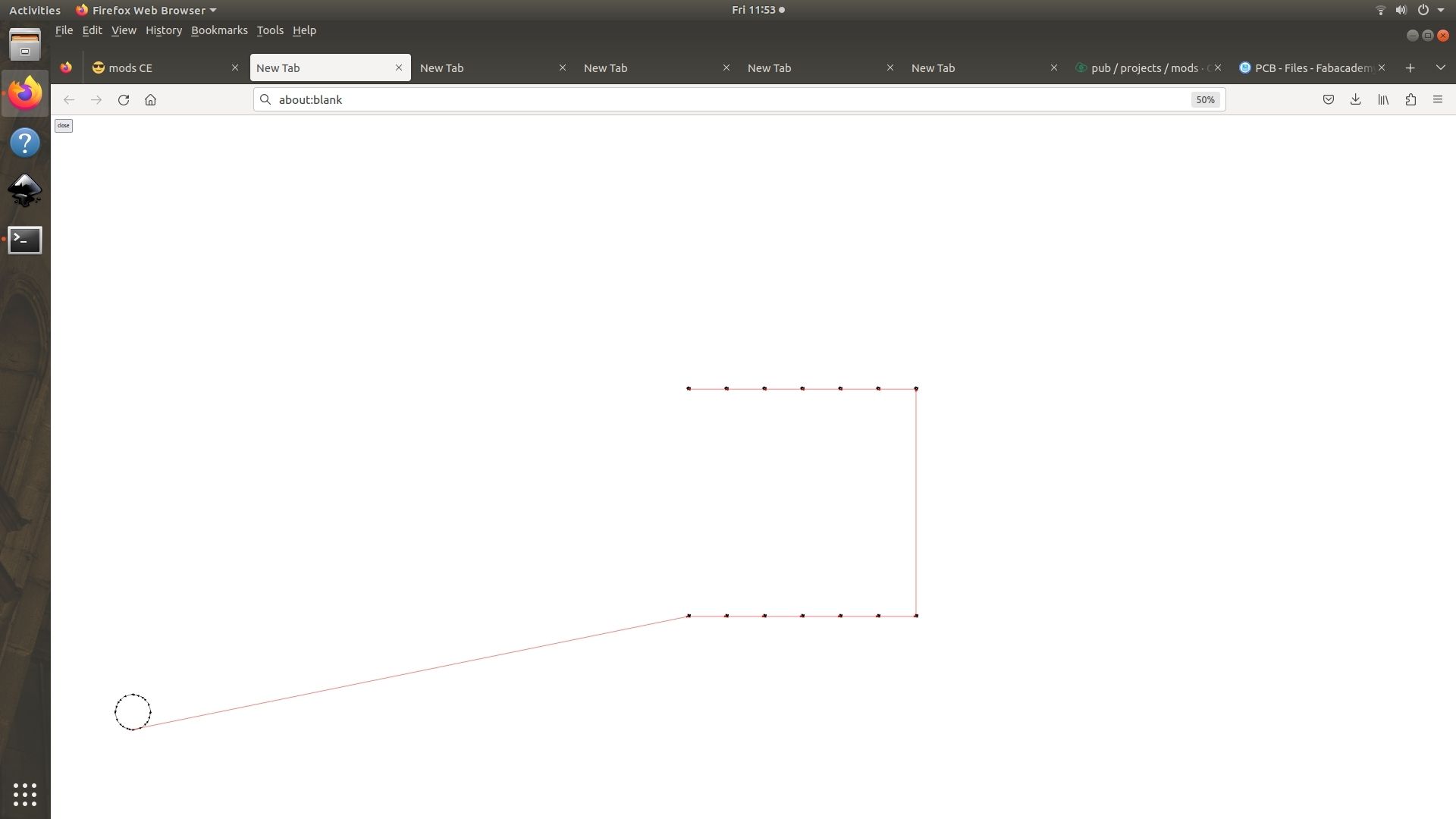
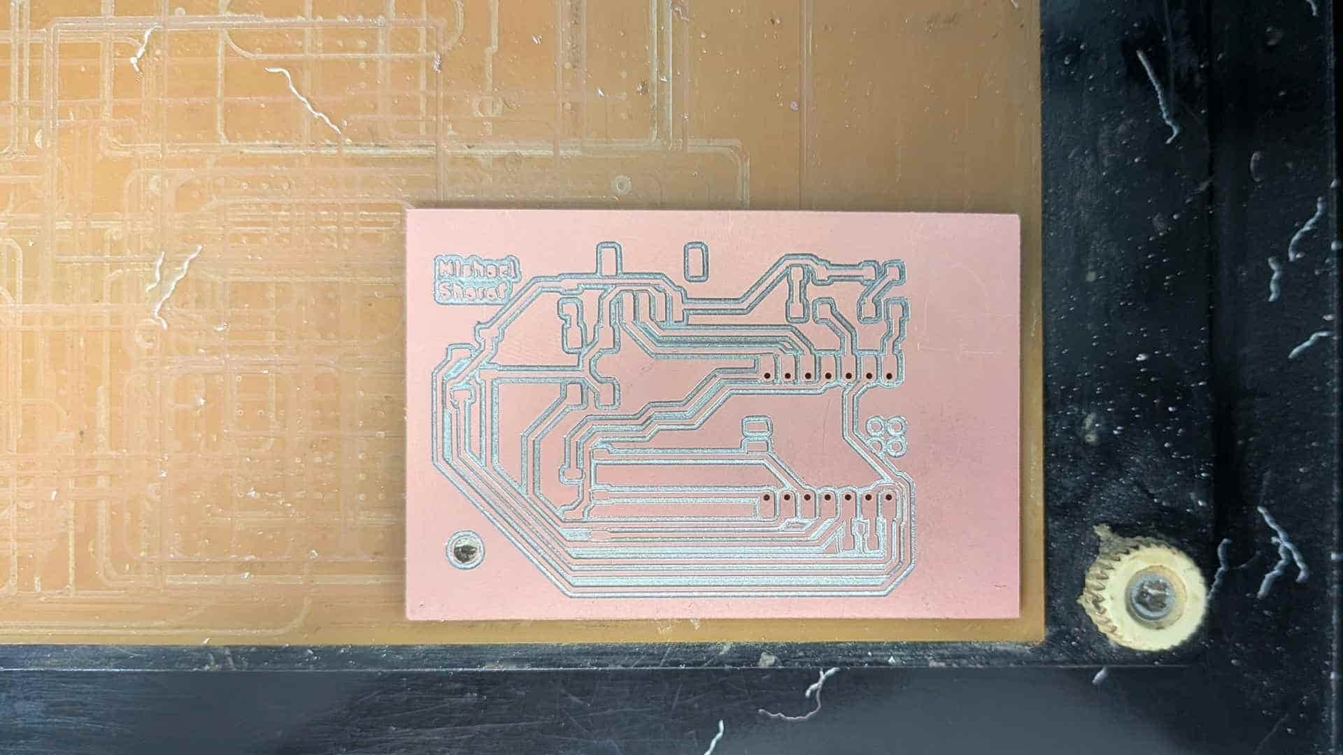
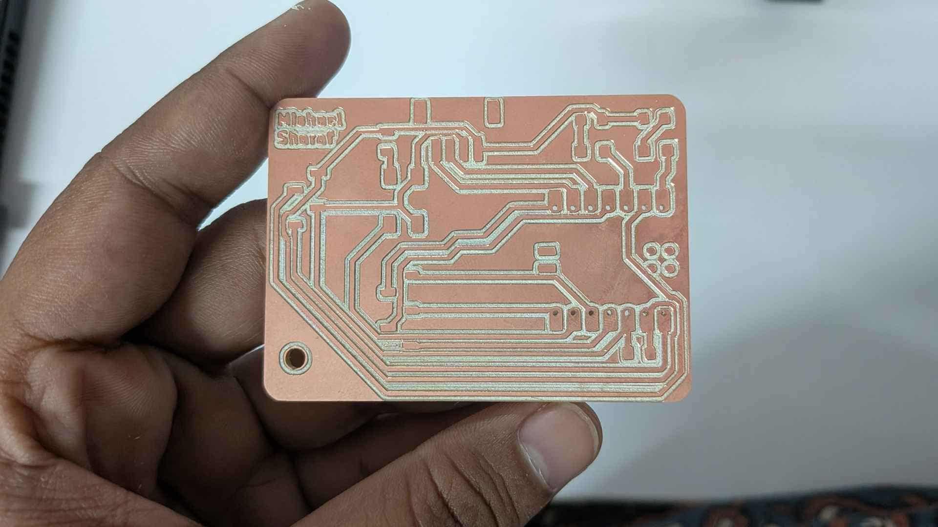
Milling Outline -Top Layer
After the drills were completed, the outline PNG file was loaded into Mods Project. For this step, the tool remained the same as used for drilling: a 0.8 mm flat end mill. The outline toolpath was then calculated and sent to the Roland Modela MDX-20 to cut the PCB board out from the stock material.

After the milling was completed on the Roland Modela MDX-20, the PCB was carefully removed from the machine bed using a scraper.
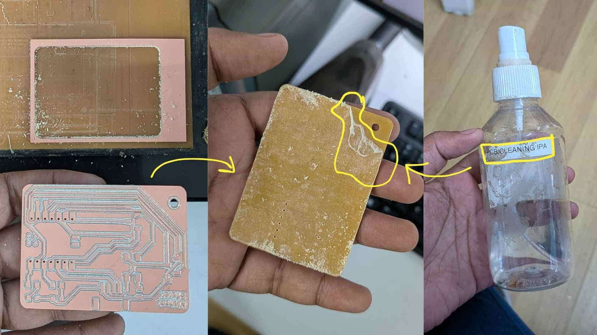
Any remaining adhesive from the double-sided tape was cleaned using an IPA (isopropyl alcohol) solution, which helped remove the sticky residue from the back of the board and left the PCB clean for the next step of assembly.
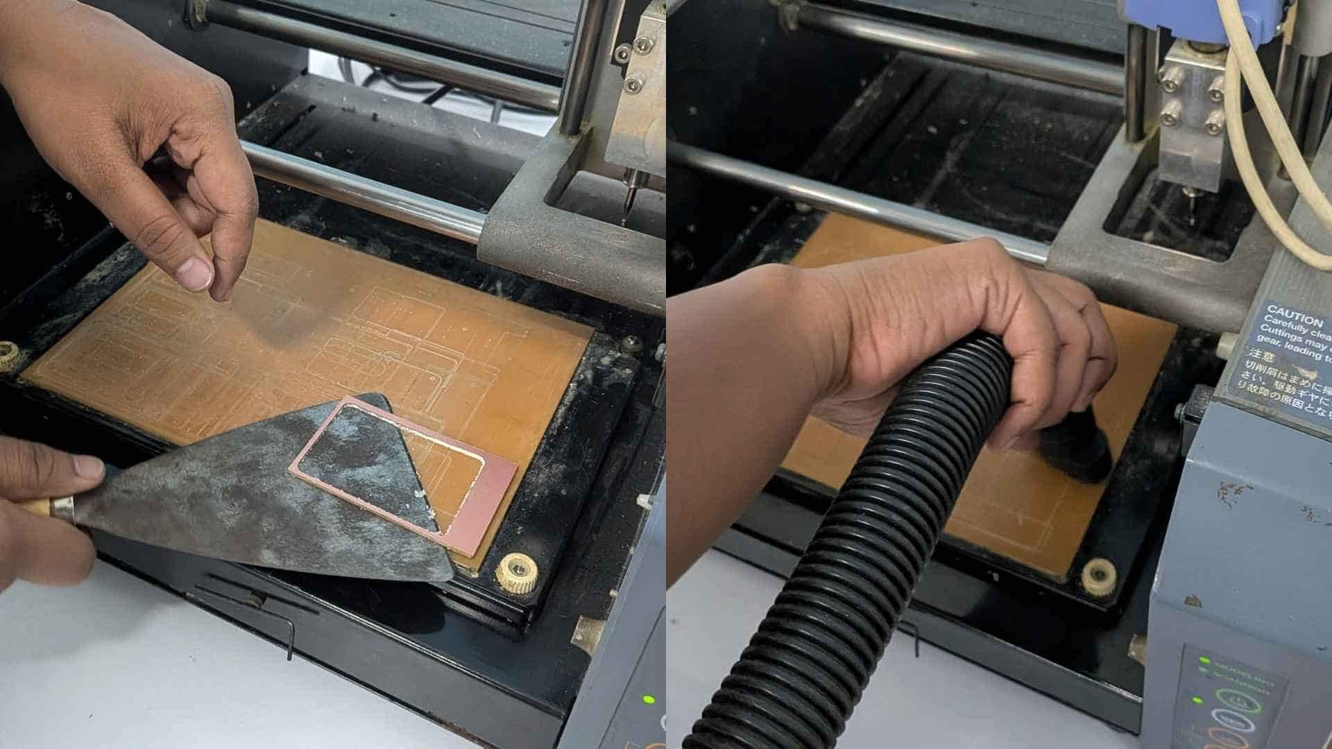
After removing the PCB, the remaining material on the machine bed was also scraped off. A vacuum was then used to clean the milling area so the Roland Modela MDX-20 bed was ready for the next user.
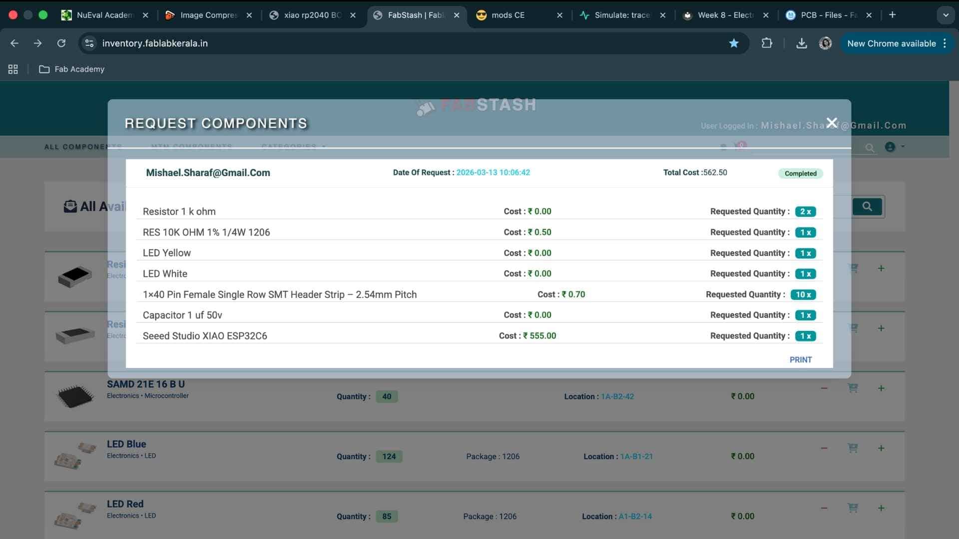
Accessing Components from the Lab Inventory (FabStash)
To obtain the electronic components required for PCB assembly, the Fab Lab Kerala inventory system called FabStash is used. This platform allows students to search the lab inventory and request components needed for their projects.
FabStash functions as a digital inventory management interface, making it easier to track available electronic components and their storage locations within the lab.
Logging into FabStash:The FabStash system can be accessed through the lab inventory portal:
inventory.fablabkerala.inAfter opening the website, users log in using their Fab Lab credentials. Once logged in, the interface displays all available electronic components stored in the lab inventory.
Searching for Components:The inventory system allows users to quickly locate components required for PCB assembly.
Using FabStash helps maintain accurate inventory records while ensuring that components are distributed efficiently among users.
Collecting Components
After milling the PCB, the required components were searched in FabStash. Most components were available in the inventory system, but the button and JST connector were not listed even though they were physically available. These were noted manually on the printed request sheet.
Once the request was approved and printed, the inventory was visited and the required components were collected from their respective storage locations.
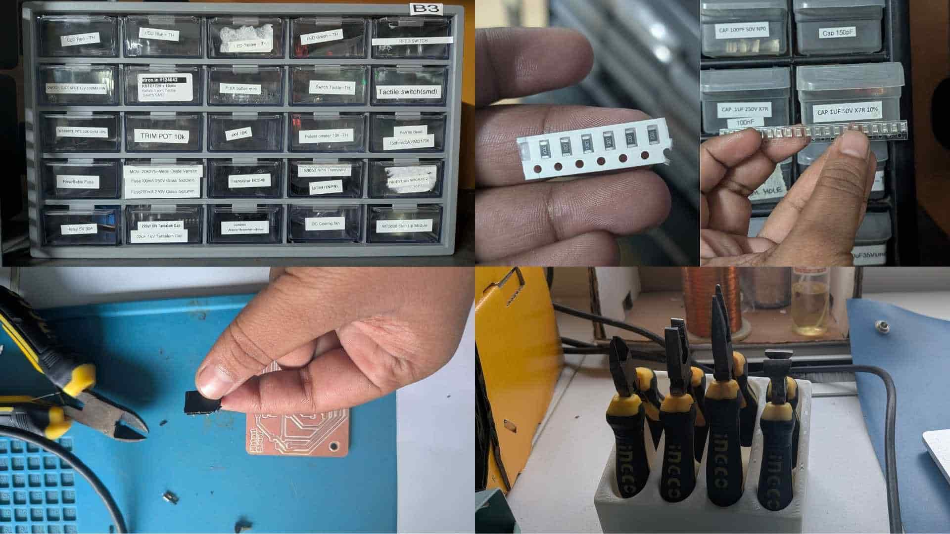

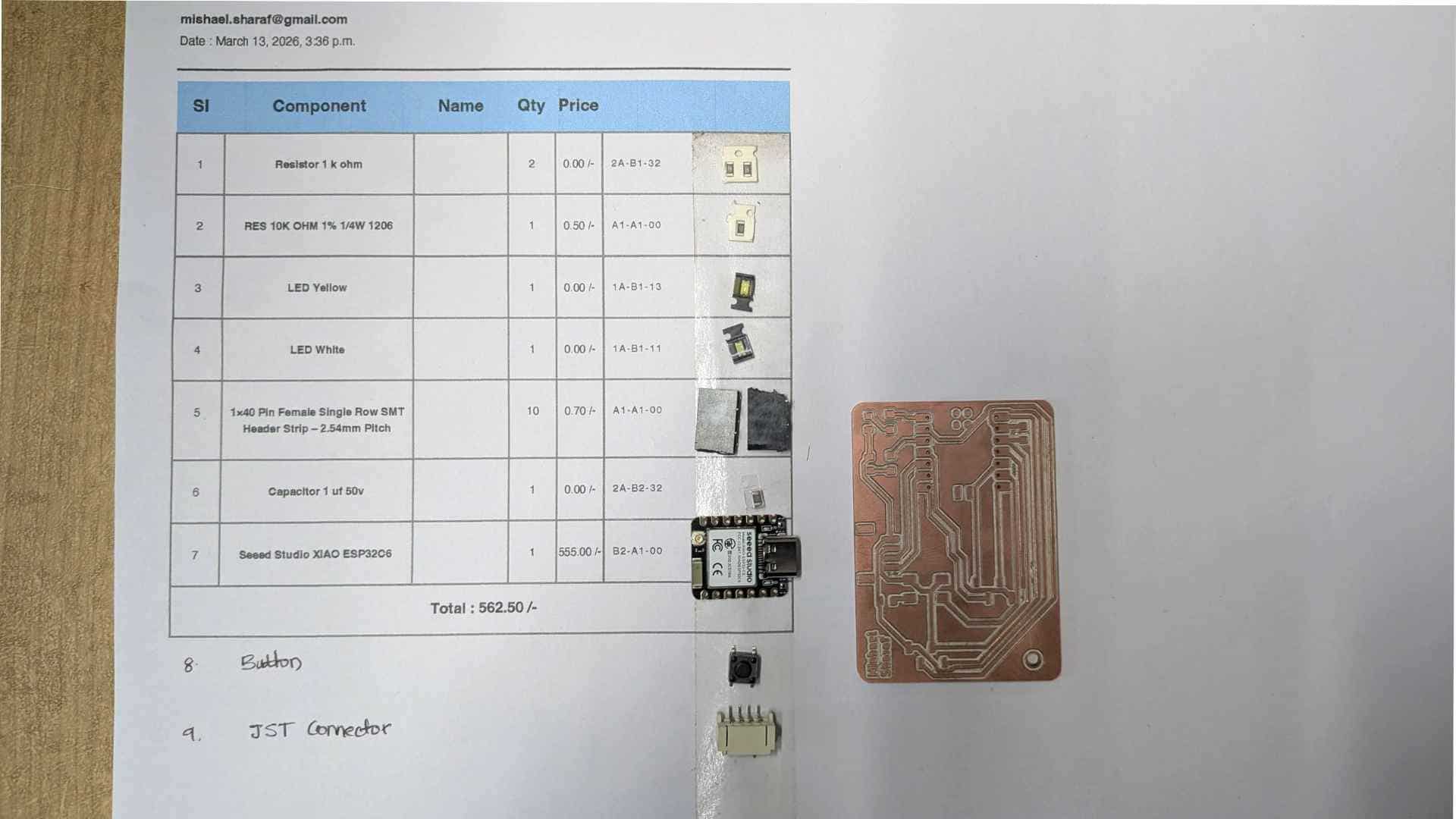
All the collected components were placed on double-sided sticky tape attached to the printed component list to keep them organized and to prevent the tiny components from getting lost. After that, I moved to the soldering station, where a brief session on soldering techniques was conducted before assembling the board.
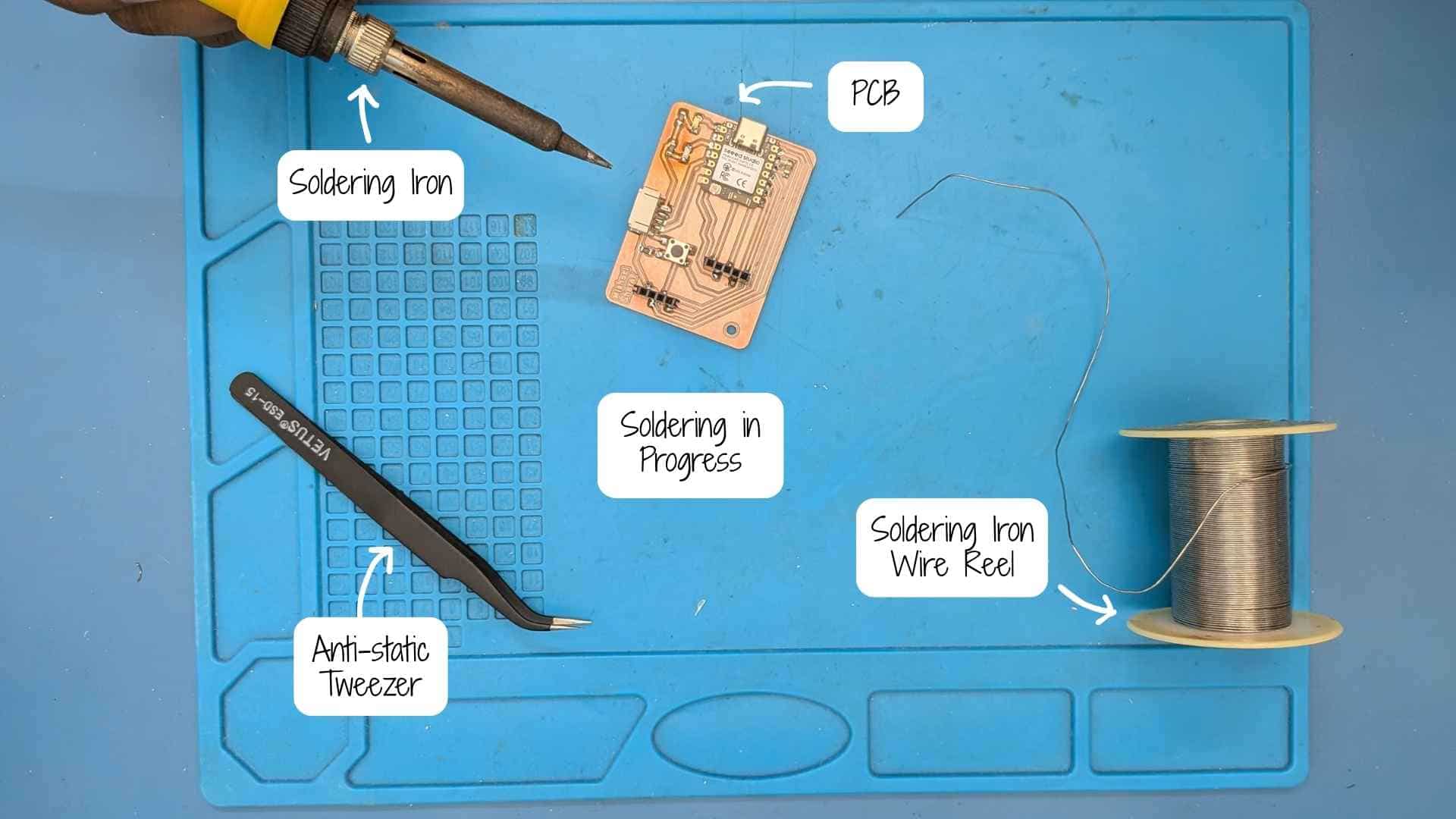
Soldering
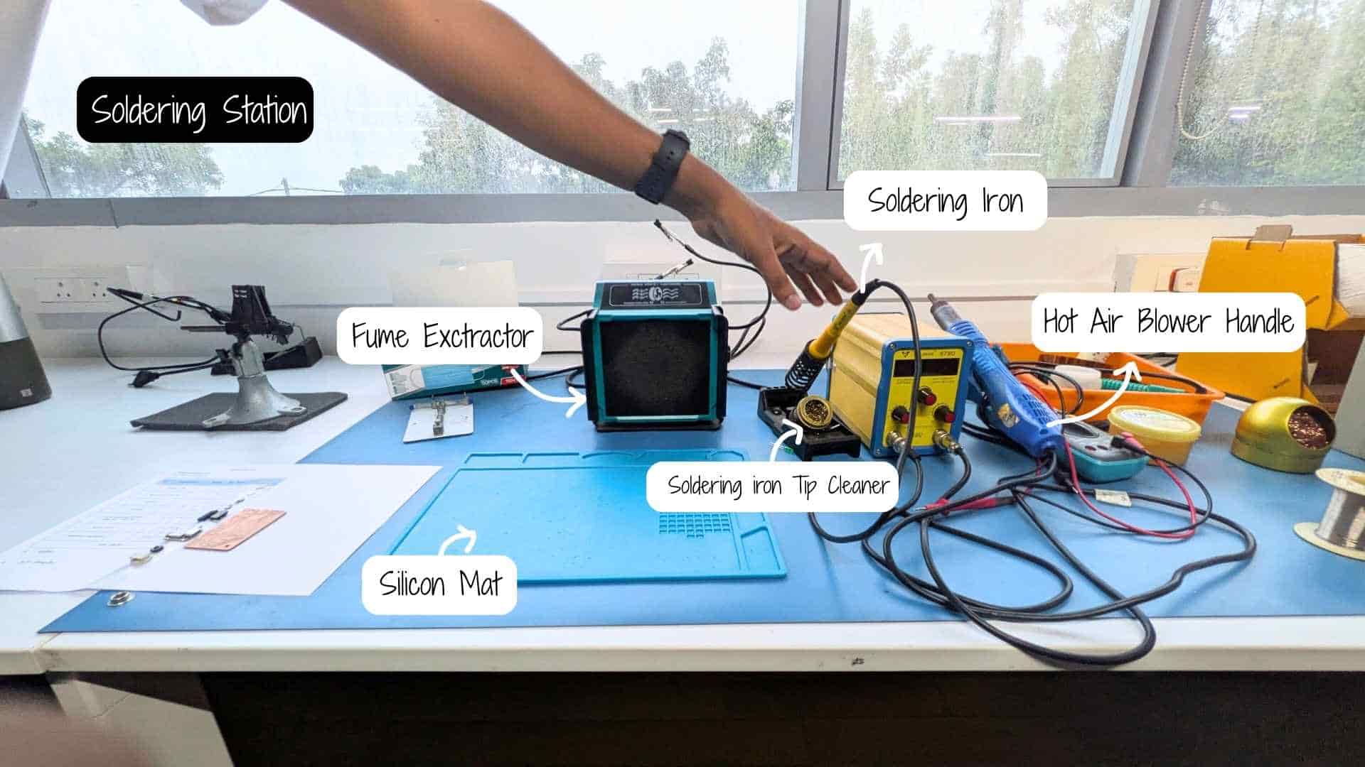
Soldering Station Setup
Before starting assembly, the basic soldering workstation setup was introduced. The station included the essential tools used for surface-mount soldering:
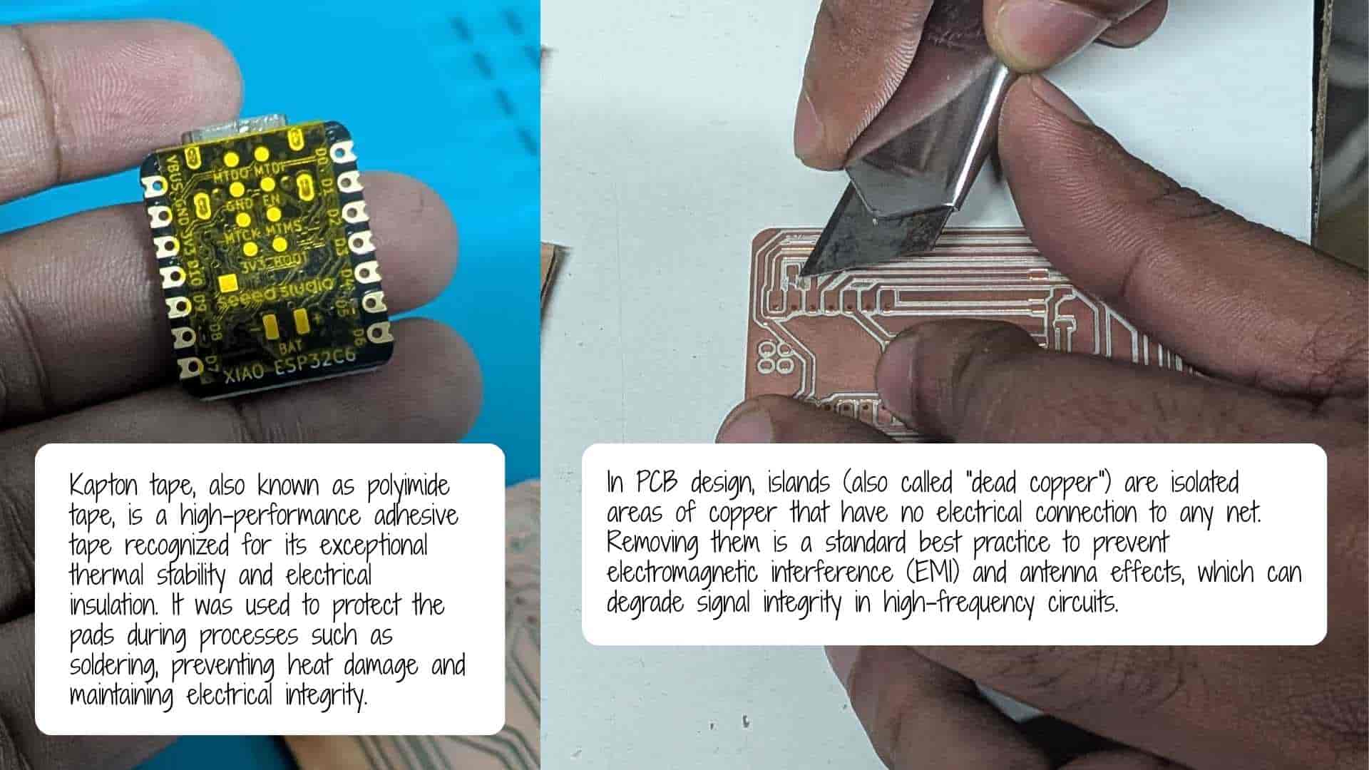
This was my second time soldering. The first time was a few weeks earlier when I soldered header pins to a Seeed Studio XIAO RP2040.
After collecting all the components, I moved to the soldering station where a short refresher session on surface-mount soldering was given before assembling the PCB.
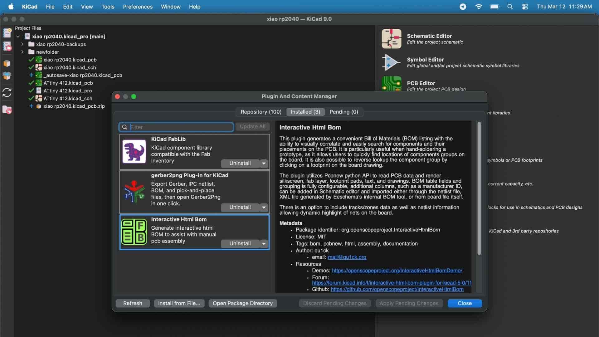
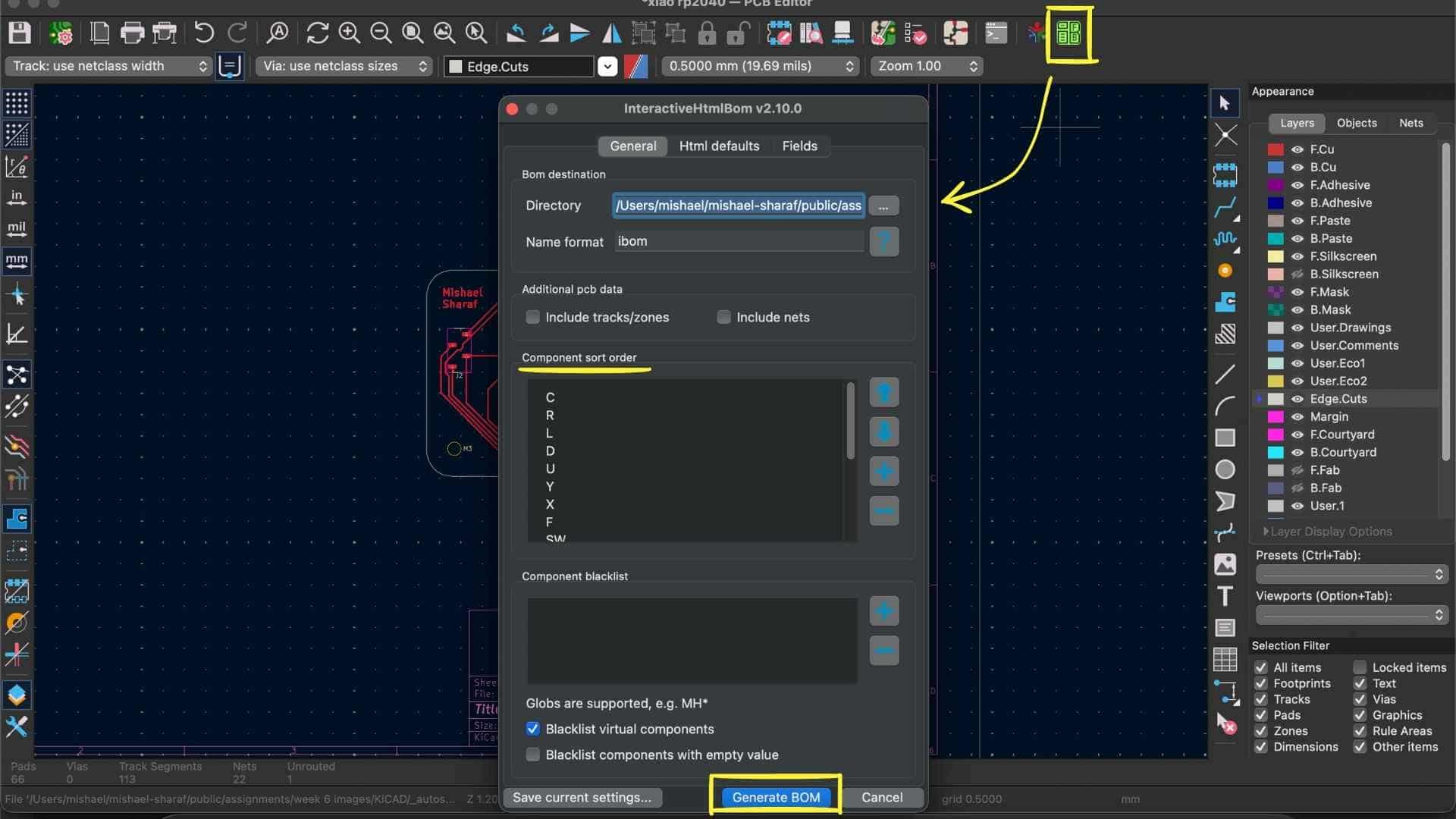
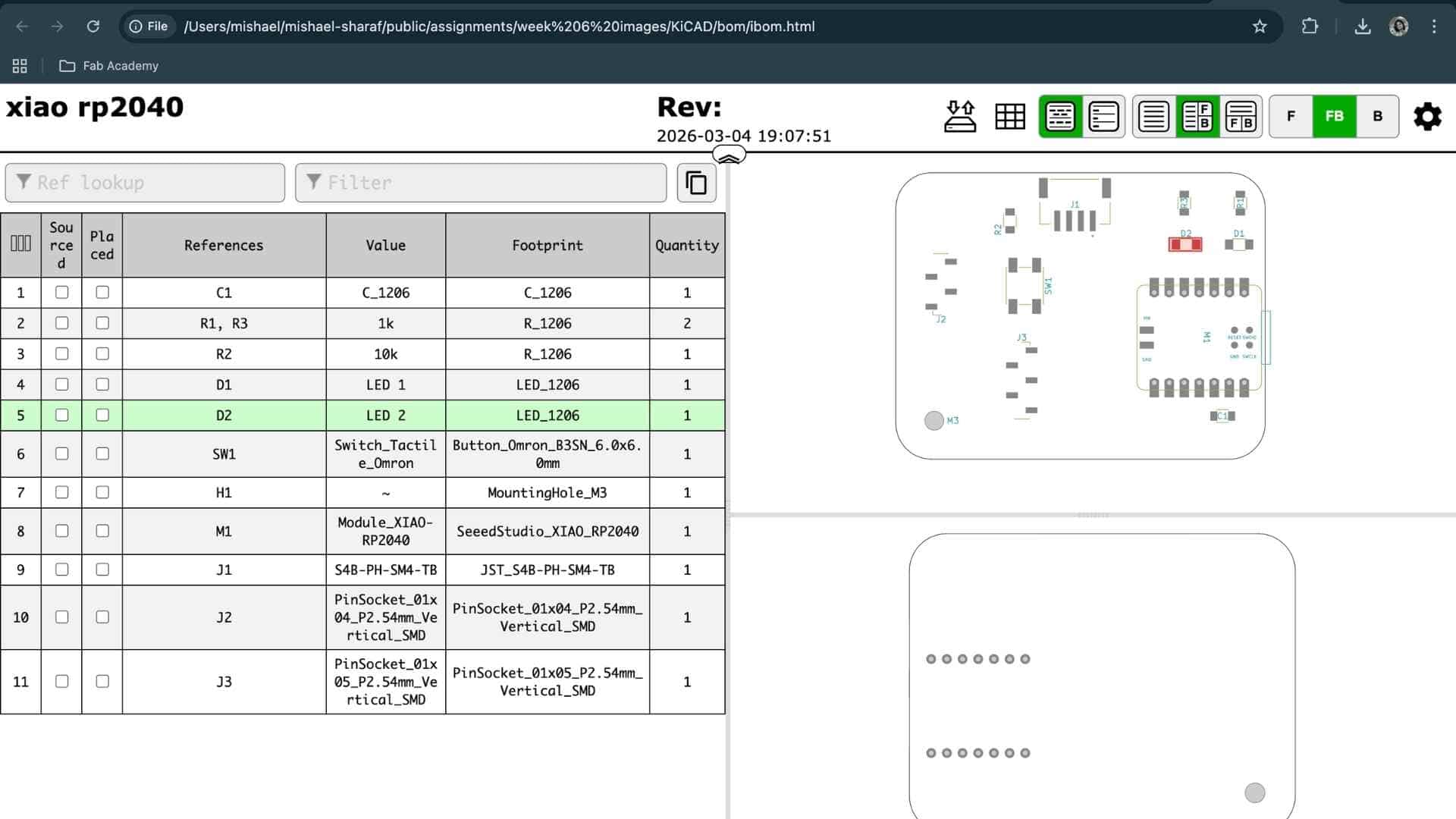
Interactive HTML BOM Plugin
The Interactive HTML BOM (iBOM) plugin was installed in KiCad to support the soldering and assembly process. It generates an interactive HTML page where each component listed in the Bill of Materials is directly linked to its exact location on the PCB layout. This makes it easier to identify, locate, and place components accurately during soldering.
Key features include:
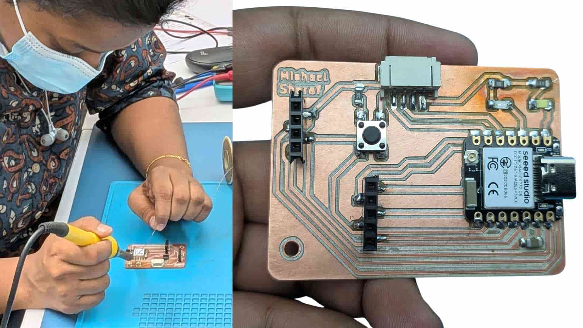
Before soldering, the PCB surface was lightly sanded/cleaned to ensure better solder adhesion. The components were then carefully soldered onto the milled board.
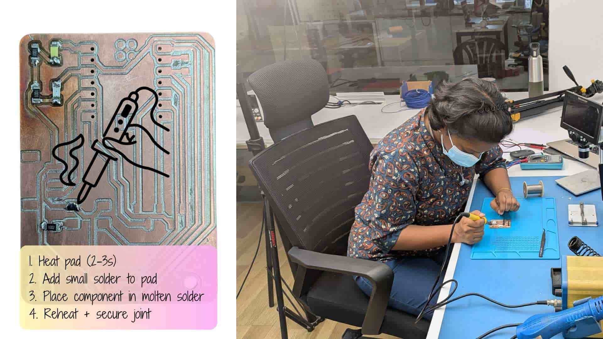
Soldering was a bit tricky at first and required patience, focus, and steady hands, especially when handling the small surface-mount components. With careful placement and controlled soldering, the components were gradually assembled onto the board.
Testing
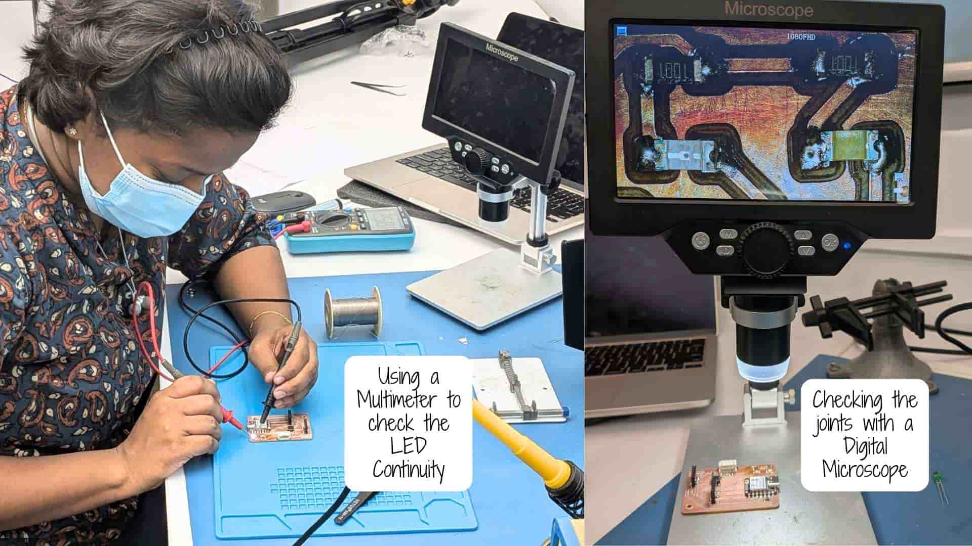
A digital microscope was also available at the soldering station to inspect the joints closely. It helped check the quality of the solder connections, identify solder bridges, and ensure that the small surface-mount components were properly aligned and connected.
After soldering the LEDs, I used a multimeter to check the continuity. Since LEDs are polarized components, incorrect orientation would prevent them from functioning. The multimeter helped verify the continuity and confirm that the LEDs were placed with the correct polarity.
Programming
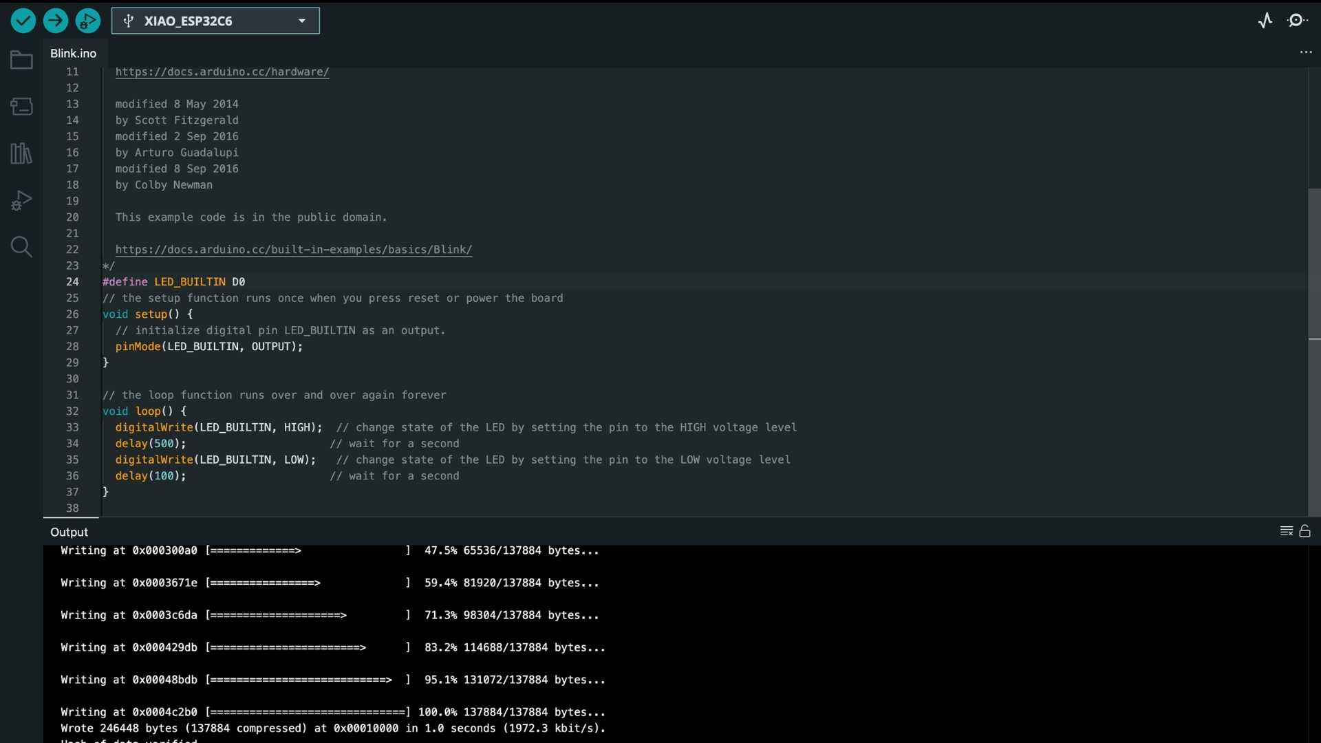
After completing the soldering, the board was tested by running a Blink LED program using Arduino IDE.
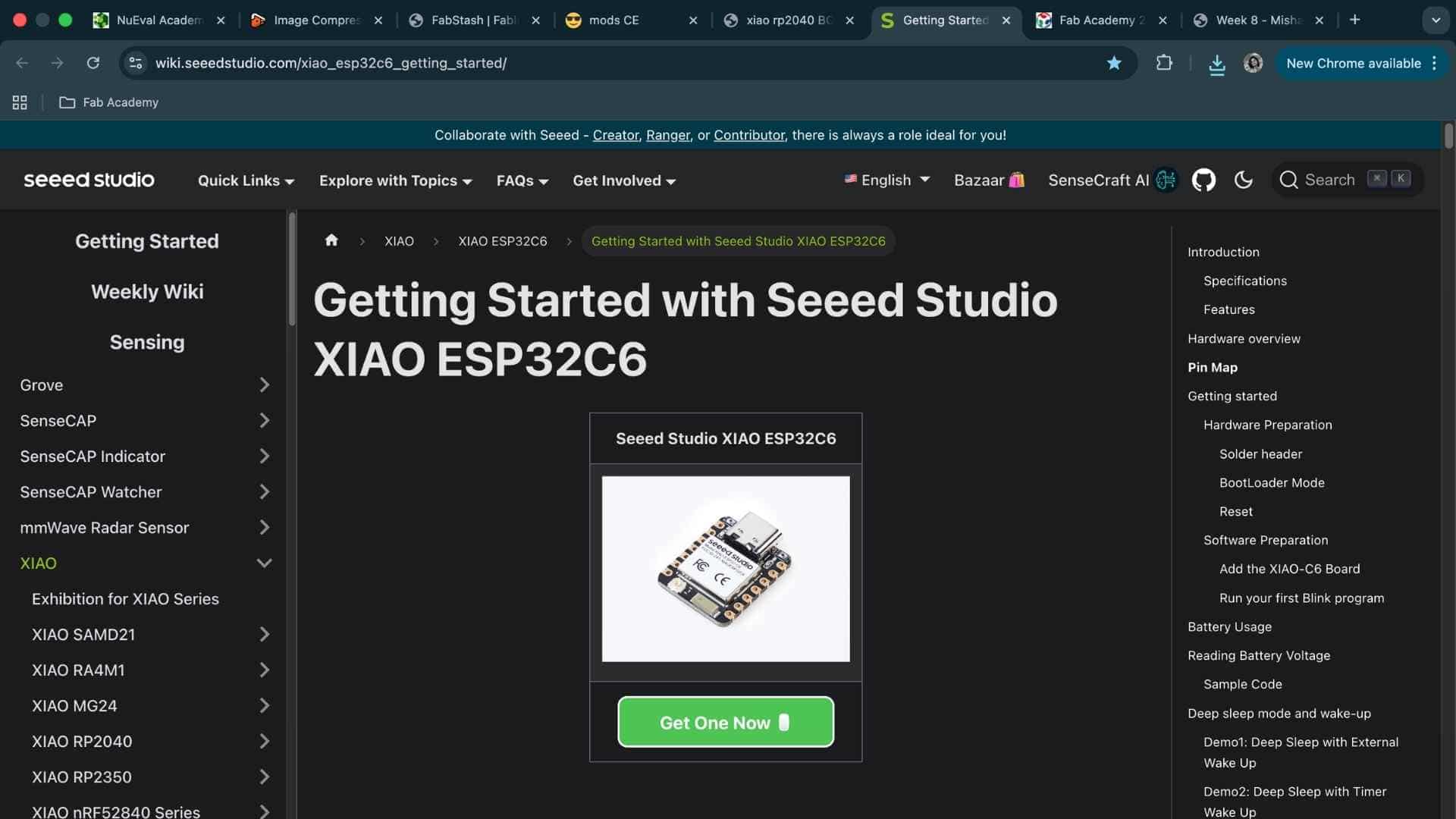
This board used the Seeed Studio XIAO ESP32C6, which required a different setup from the Seeed Studio XIAO RP2040 that I had previously used.
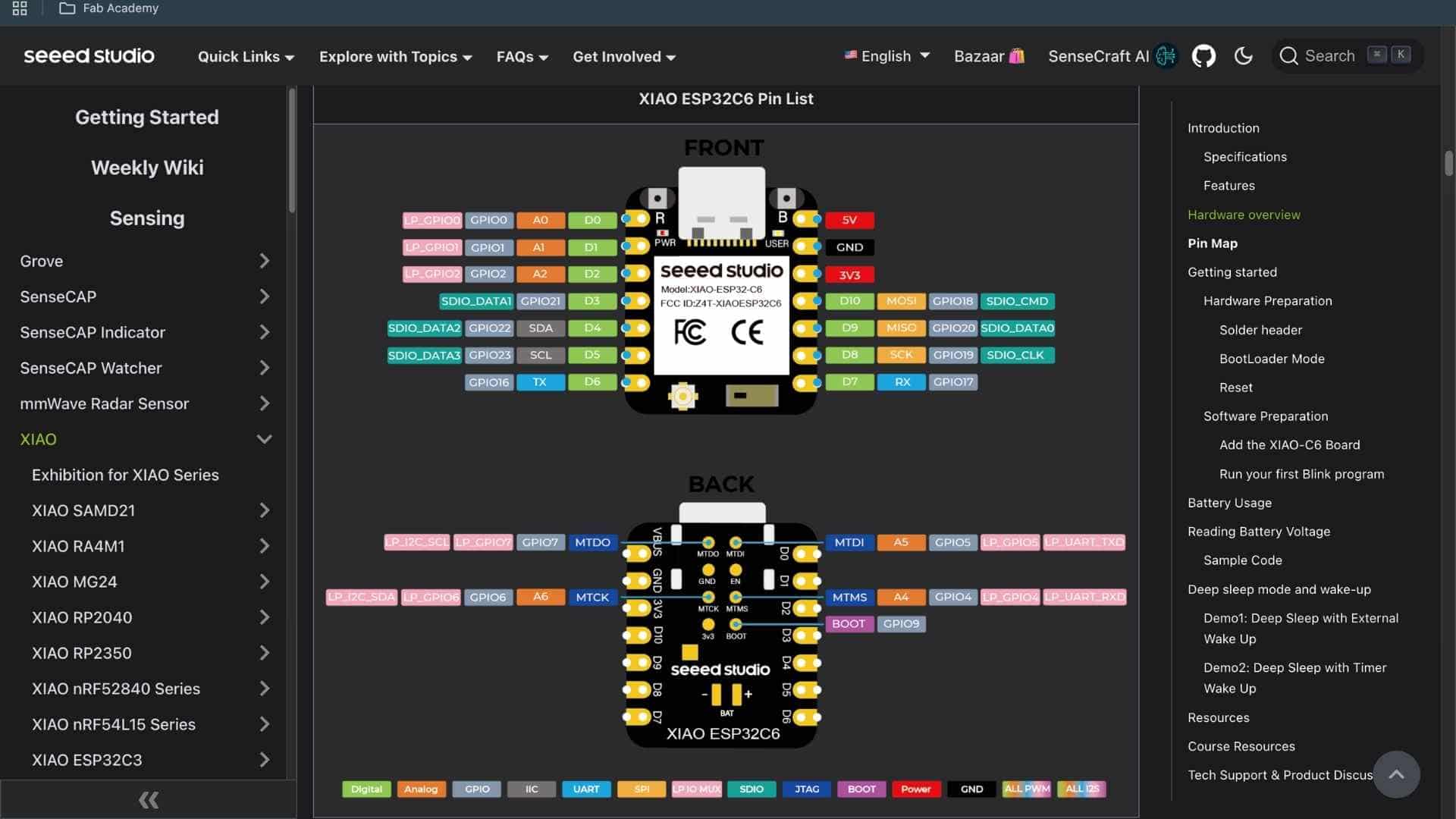
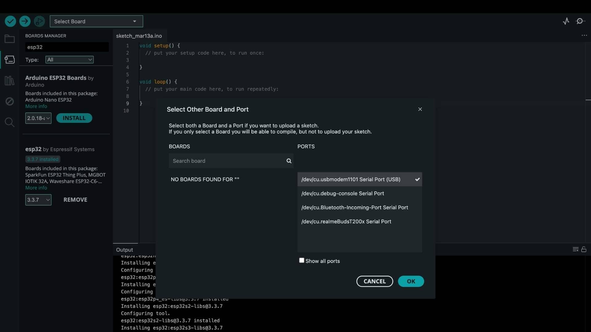
To configure the board, I followed the setup guide from Seeed Studio.
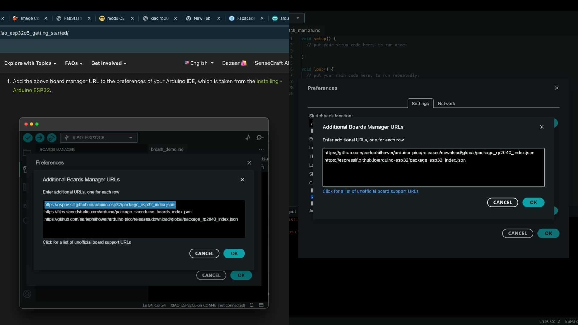
The required board package was installed, the correct board and port were selected in the Arduino IDE, and the Blink example program was uploaded.
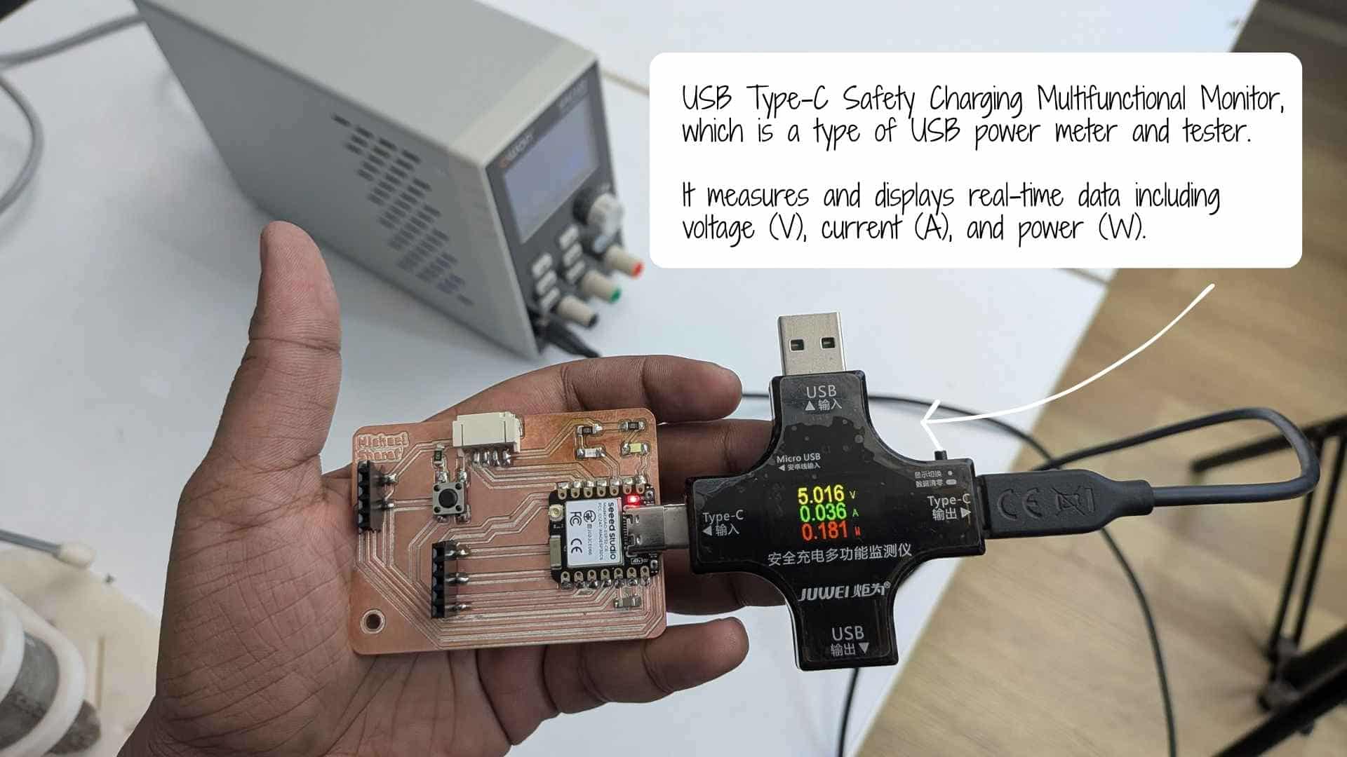
After uploading the program, the LED blinked as expected, confirming that the PCB was successfully fabricated, soldered, and functioning correctly.

Visual Pin Mapping on the PCB for Programming reference
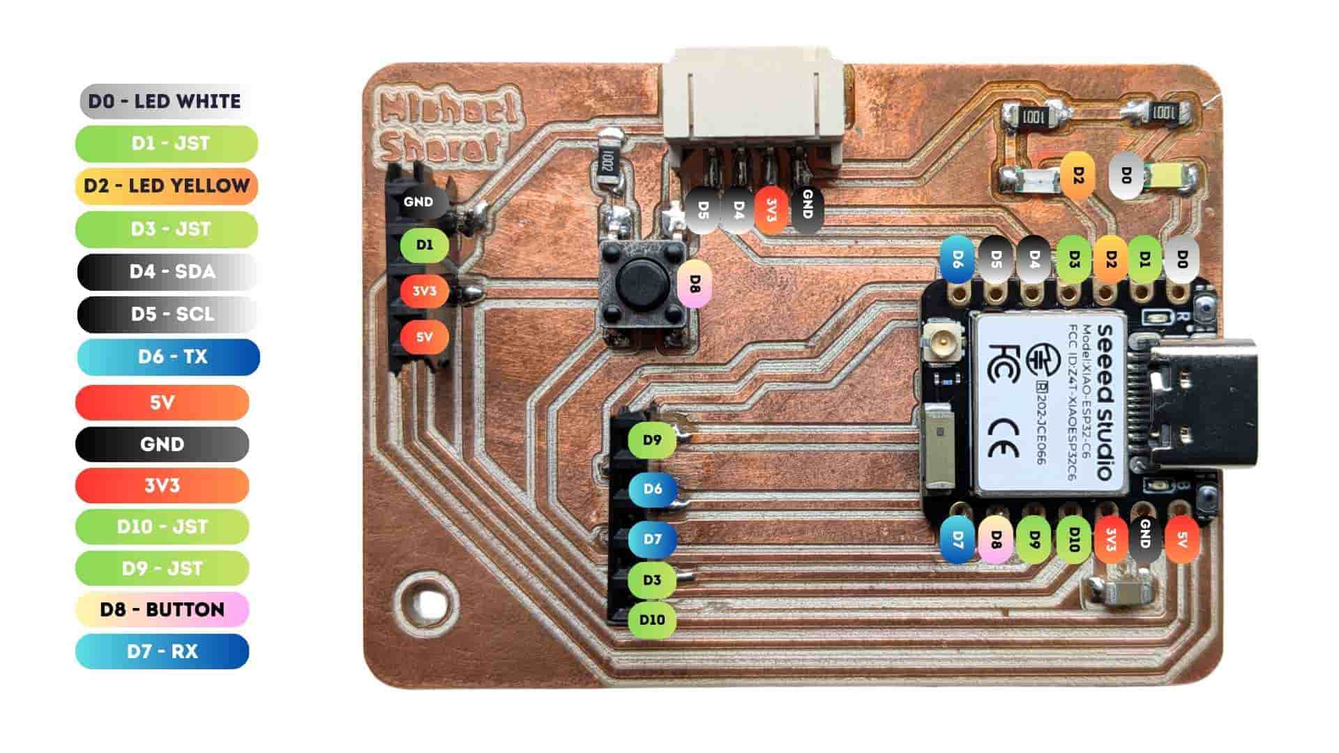
#define LED_BUILTIN D0
// the setup function runs once when you press reset or power the board
void setup() {
  // initialize digital pin LED_BUILTIN as an output.
  pinMode(LED_BUILTIN, OUTPUT);
}

// the loop function runs over and over again forever
void loop() {
  digitalWrite(LED_BUILTIN, HIGH);  // change state of the LED by setting the pin to the HIGH voltage level
  delay(500);                      // wait for a second
  digitalWrite(LED_BUILTIN, LOW);   // change state of the LED by setting the pin to the LOW voltage level
  delay(100);                      // wait for a second
}
Hero Shot

I took the programs from week 4, updated the pin numbers according to my PCB schematic, and ran the code; while I verified the basic LED blinking, I also wanted to test the button input and serial monitor programs.
LED Chase with Push Button
// Define names for each LED pin
#define YELLOW D2
#define WHITE  D0


// Define button pin
#define BUTTON D8

// Time delay between LED changes (in milliseconds)
#define time   100

// Store all LED pins inside an array
// This lets us control them using a loop
int leds[] = {YELLOW, WHITE};

// Total number of LEDs in the array
int numLeds = 2;

void setup() {

  // Set all LED pins as OUTPUT (they send voltage out)
  pinMode(YELLOW, OUTPUT);
  pinMode(WHITE, OUTPUT);


  // Set button as INPUT with internal pulldown resistor
  // When pressed, reads HIGH
  // When not pressed, reads LOW
  pinMode(BUTTON, INPUT_PULLDOWN);
}

void loop() {

  // Check if button is pressed
  if (digitalRead(BUTTON) == HIGH) {

  // If pressed, run LED chase pattern
    chase_2();
  }
  else {

  // If not pressed, turn all LEDs OFF
  // Loop goes through each LED one by one
    for (int i = 0; i < numLeds; i++) {

  // leds[i] selects LED number 0,1,2,3
      digitalWrite(leds[i], LOW);
    }
  }
}

// Function to run LEDs one after another
void chase_2() {

  // Loop through each LED
  for (int i = 0; i < numLeds; i++) {

  // Turn current LED ON
    digitalWrite(leds[i], HIGH);

  // Wait for defined time
    delay(time);

  // Turn current LED OFF before moving to next
    digitalWrite(leds[i], LOW);
  }
}
Push Button & Serial Monitor
#define BUTTON D8

int lastState = HIGH;

void setup() {
  pinMode(BUTTON, INPUT_PULLUP);
  Serial.begin(9600);
}

void loop() {

  int currentState = digitalRead(BUTTON);

  if (lastState == HIGH && currentState == LOW) {
    Serial.println("Ouch, that hurts!");
  }

  lastState = currentState;
}
Push Button, LED & Serial Monitor
#define LED_PIN D0
#define BUTTON_PIN D8

bool blinking = false;
bool lastButtonState = LOW;   // Default state is LOW with pull-down
bool ledState = LOW;

unsigned long previousMillis = 0;
const long interval = 500;

void setup() {
  pinMode(LED_PIN, OUTPUT);
  pinMode(BUTTON_PIN, INPUT_PULLDOWN);  // Internal pull-down enabled

  Serial.begin(9600);
}

void loop() {

  bool currentButtonState = digitalRead(BUTTON_PIN);

  // Detect rising edge (LOW → HIGH)
  if (lastButtonState == LOW && currentButtonState == HIGH) {

    blinking = !blinking;   // Toggle blinking mode

    if (blinking) {
      Serial.println("ITS ON BABE");
    } else {
      Serial.println("ITS OFF BABE");
      digitalWrite(LED_PIN, LOW);
      ledState = LOW;
    }

    delay(50); // debounce
  }

  lastButtonState = currentButtonState;

  if (blinking) {
    unsigned long currentMillis = millis();

    if (currentMillis - previousMillis >= interval) {
      previousMillis = currentMillis;

      ledState = !ledState;
      digitalWrite(LED_PIN, ledState);
    }
  }
}
Button Controlled Brightness
#define LED_PIN D0
#define BUTTON_PIN D8

int brightness = 0;
int stepSize = 64;

bool lastButtonState = HIGH;

void setup() {
  pinMode(LED_PIN, OUTPUT);
  pinMode(BUTTON_PIN, INPUT_PULLUP);
}

void loop() {

  bool currentButtonState = digitalRead(BUTTON_PIN);

  if (lastButtonState == HIGH && currentButtonState == LOW) {

    brightness += stepSize;

    if (brightness > 255) {
      brightness = 0;
    }

    analogWrite(LED_PIN, brightness);

    delay(50); // debounce
  }

  lastButtonState = currentButtonState;
}
Insights
This week made me realize how sensitive the transition from digital design to physical making actually is. Even something as small as a drill size matching the tool diameter caused a real issue, and fixing it meant going back and understanding what was actually happening instead of just trying things randomly.
It also made the whole process feel more connected. Designing, milling, soldering, and testing are not separate steps, each one depends on the previous one being done right. It made me slow down, pay attention, and be more careful with decisions throughout the workflow.
Source Files
References
To better understand PCB structure and fabrication, I referred to the following resources: