Week 11: Communication and Networking
Objectives
Individual Assignment
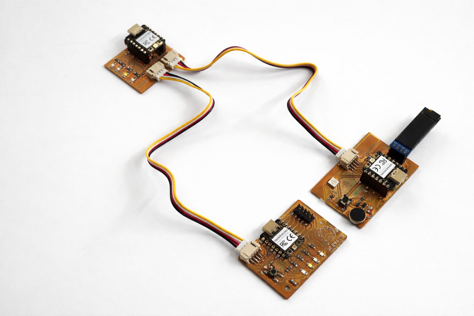
This week focuses on networking and communication. The goal is to build a network with 1 Master and 2 Nodes to get multiple microcontroller boards talking to each other.
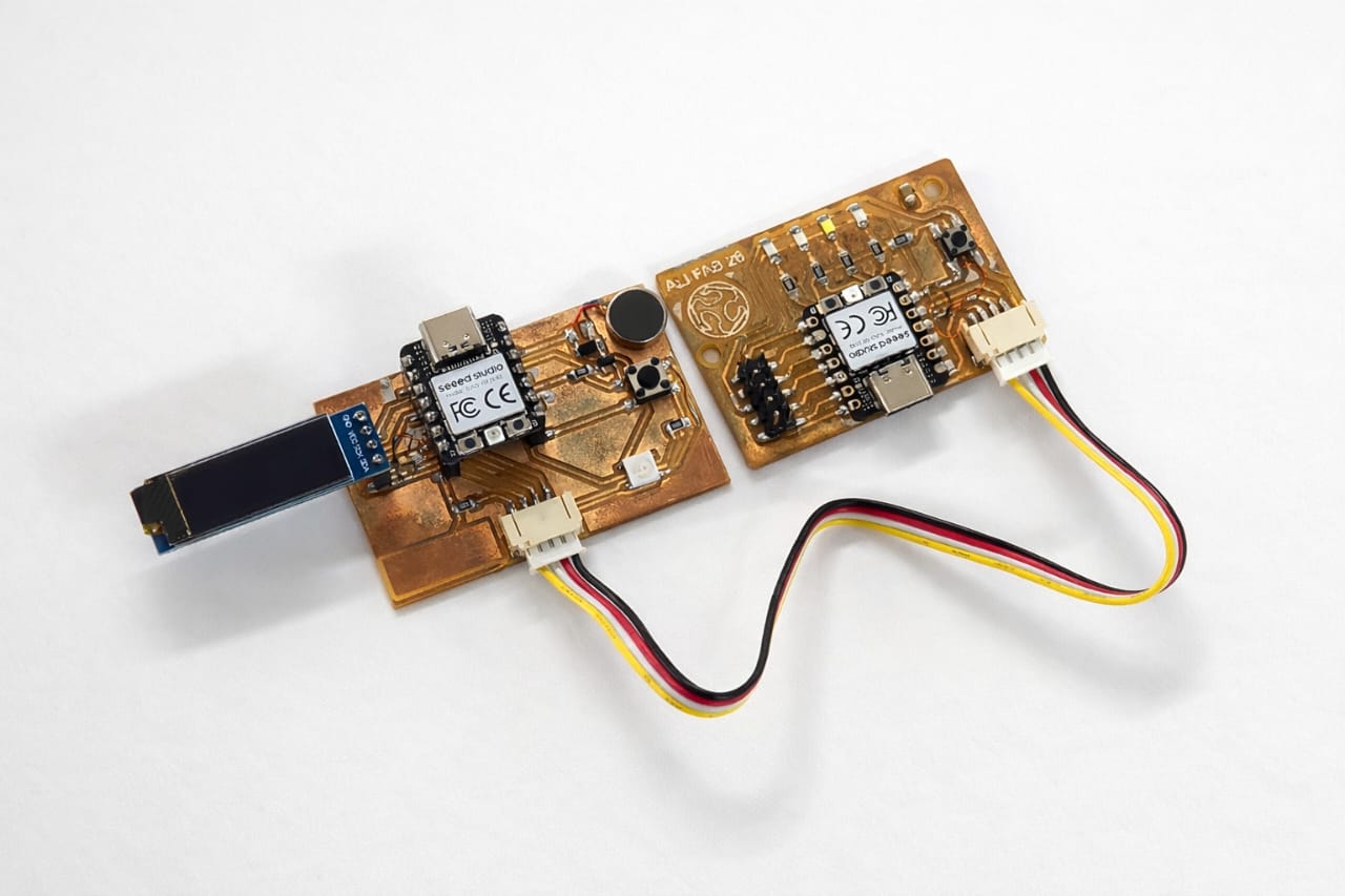
To do this, I am connecting three boards together:
- My existing PCB from Week 06
- My existing PCB from Week 10
- A new PCB designed and fabricated this week to act as Node 2
Below, I introduce each board, explain the I2C wiring, and document the programming process used to handle the addressing between them.
I2C Communication
IIC or I2C is short form of Inter-Integrated Circuits,It's a type protocol to communicate in between Integrated circuits,Microcontrollers,sensors etc.. just like USB in Computers.there are many communication peripheral available for Microcontrollers.Most of the Microcontrollers have two or more different type of protocols. The advantages of I2C is most of the Devices supports the protocol and very easy to use two wire required for data and clock.
 Source
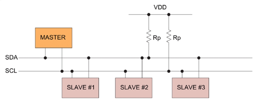
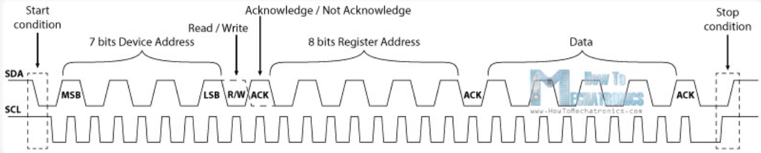
The above figure shows how a simple I2C Network look like.One device act as Master others are called slaves,and bidirectional data transfer are possible with the permission of the master device.The pins that required for this communication protocol are the SDA (Serial Data) and THe SCL (Serial Clock)
AI Image Prompt
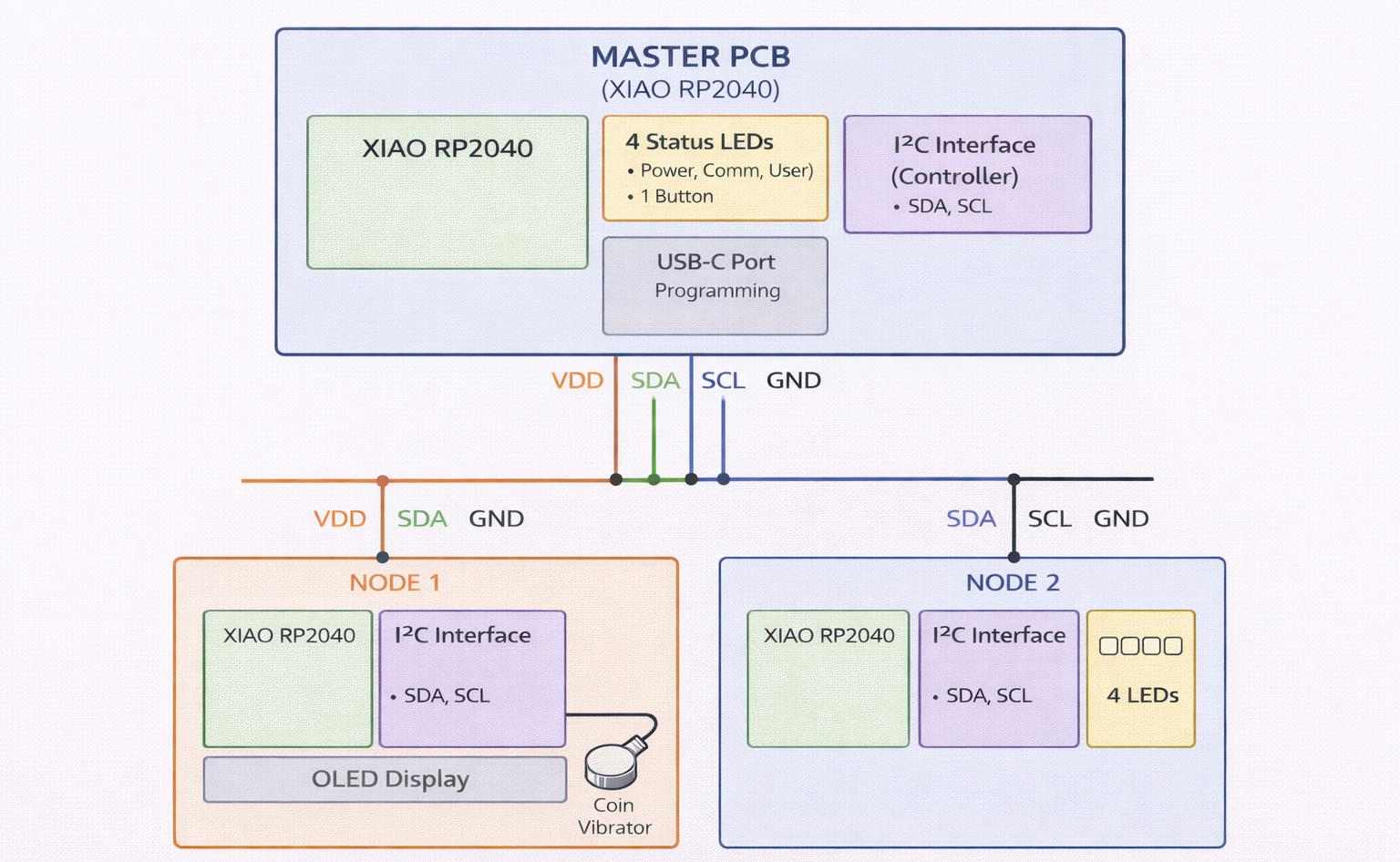
chat gpt prompt: I lost original prompt of this code. I told "Genarate code. For week network and comunication iam try to communicate between 1 master and 2 nodes i2c communication 3of them are using xiaorp 2040 controller,in master there is 4 leds and 1 button,in node 1 consist 1oled and 1 coin vibrator,in node 2 there is only 4ledsmake a block diagram of it"
AI Tool Used: ChatGPT
Each devices in the I2C bus has it's own addresses,it possible to connect almost upto upto 128(112) devices when using 7 bits addressing and almost upto 1024(1008)devices when using the 8 bits addressing
 SOURCE
Master Board – LED Chaser (Week 08)
For the master device, I used my Week 08 PCB (LED Chaser board). This board acts as the controller and sends commands to the slave nodes.
Week 08 Link: View Week 08 Documentation
Master Board Image
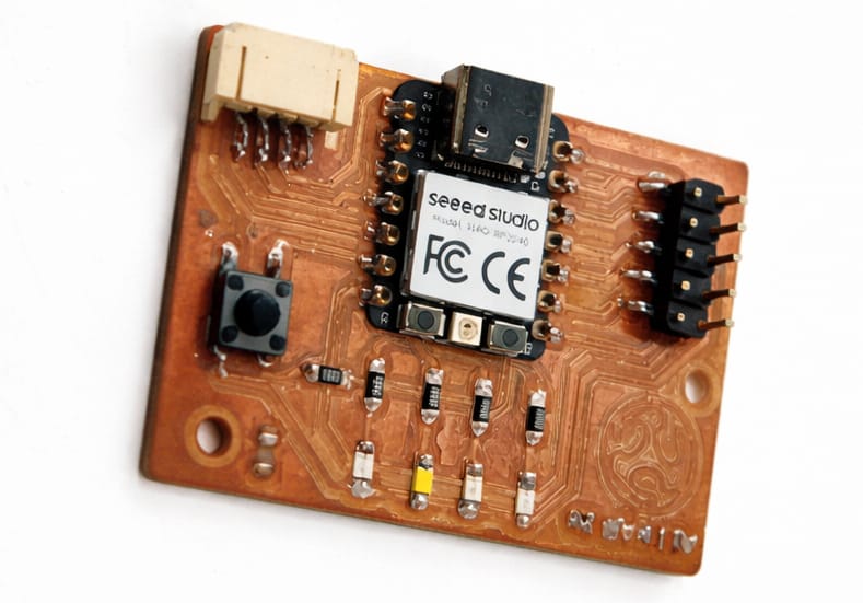
Board Overview:
- Microcontroller: Seeed Studio XIAO RP2040
- Outputs: 4 LEDs
- Inputs: 1 Push button
- Communication: I2C port
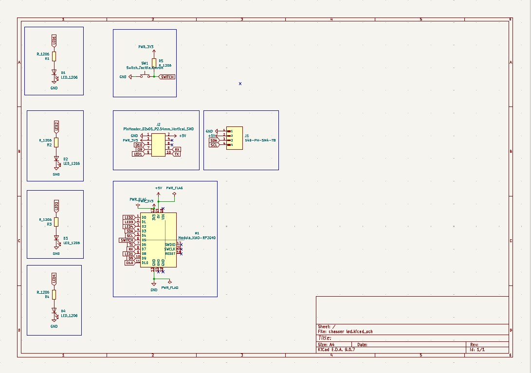
schematic Diagram
Below is the schematic diagram for my Week 08 PCB, showing the circuit layout and pin configurations.
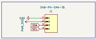
I2C Pins
this is i2c pin i used and this standered i used to entire board
- SDA (Serial Data Line) – Used to transfer data
- SCL (Serial Clock Line) – Used for clock synchronization
- GND – Common ground
I2C Pin Diagram
Master Code
#include <Wire.h>

int leds[] = {2,3,4,5};

void setup() {
  Wire.begin();

  for(int i=0;i<4;i++){
    pinMode(leds[i], OUTPUT);
  }
}

void loop() {

  for(int i=0;i<4;i++){
    digitalWrite(leds[i], HIGH);
    delay(200);
    digitalWrite(leds[i], LOW);
  }

  Wire.beginTransmission(0x08);
  Wire.write(1);
  Wire.endTransmission();

  Wire.beginTransmission(0x09);
  Wire.write(1);
  Wire.endTransmission();

  delay(1000);
}
Master Working Video
Node 1
For Node 1, I used my Week 10 output device PCB (Vibrator). This board acts as a slave device and responds to commands from the master.
Week 10 Link: View Week 10 Documentation
Below is the schematic diagram for my Week 10 PCB, showing the circuit layout and pin configurations
Node 1 Overview:
- Display: 1 OLED display
- Actuator: 1 vibration motor
Node 1
Node 1 Code
#include <Wire.h>

#define SLAVE_ADDRESS 0x08
#define MOTOR_PIN 2

void setup() {
  pinMode(MOTOR_PIN, OUTPUT);
  Wire.begin(SLAVE_ADDRESS);
  Wire.onReceive(receiveEvent);
}

void loop() {}

void receiveEvent(int x) {
  int cmd = Wire.read();

  if(cmd == 1){
    digitalWrite(MOTOR_PIN, HIGH);
    delay(500);
    digitalWrite(MOTOR_PIN, LOW);
  }
}
Node 1 Working Video
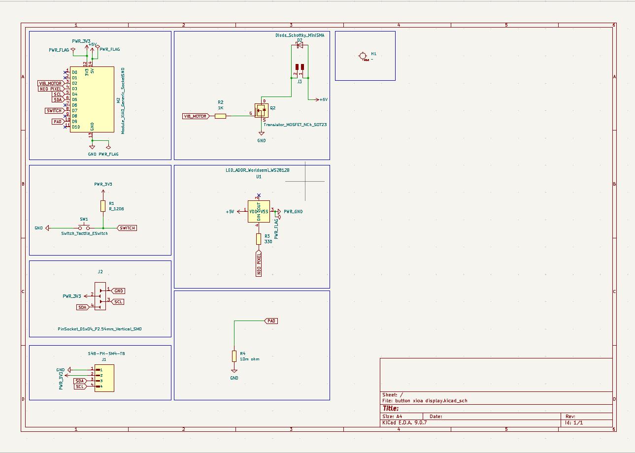
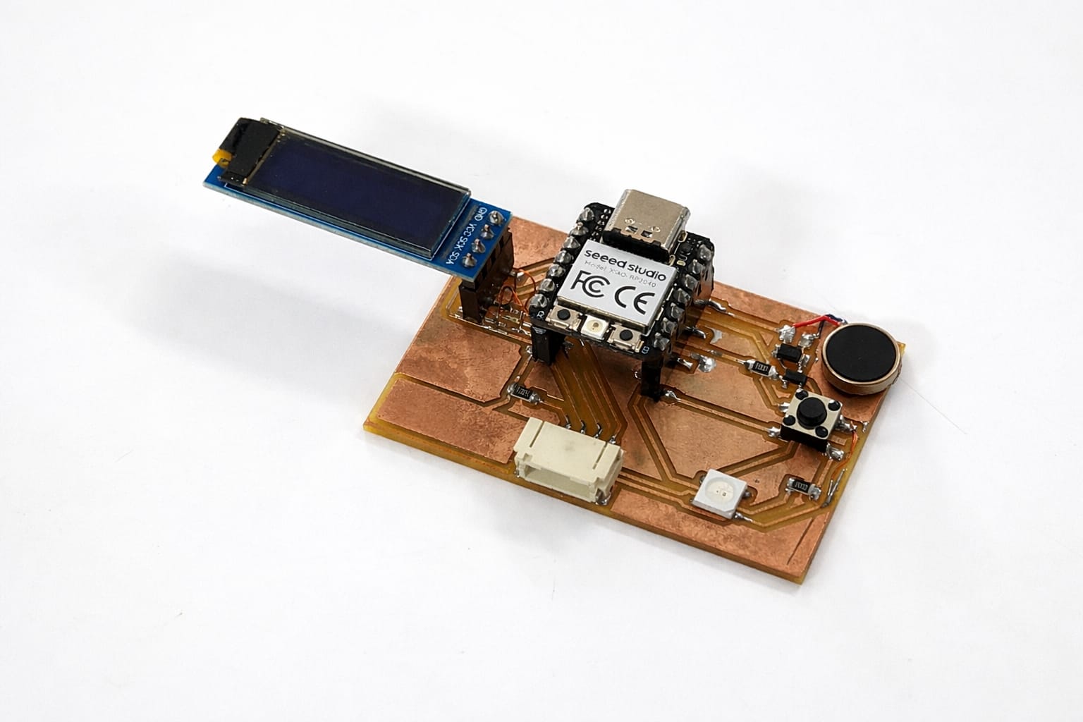
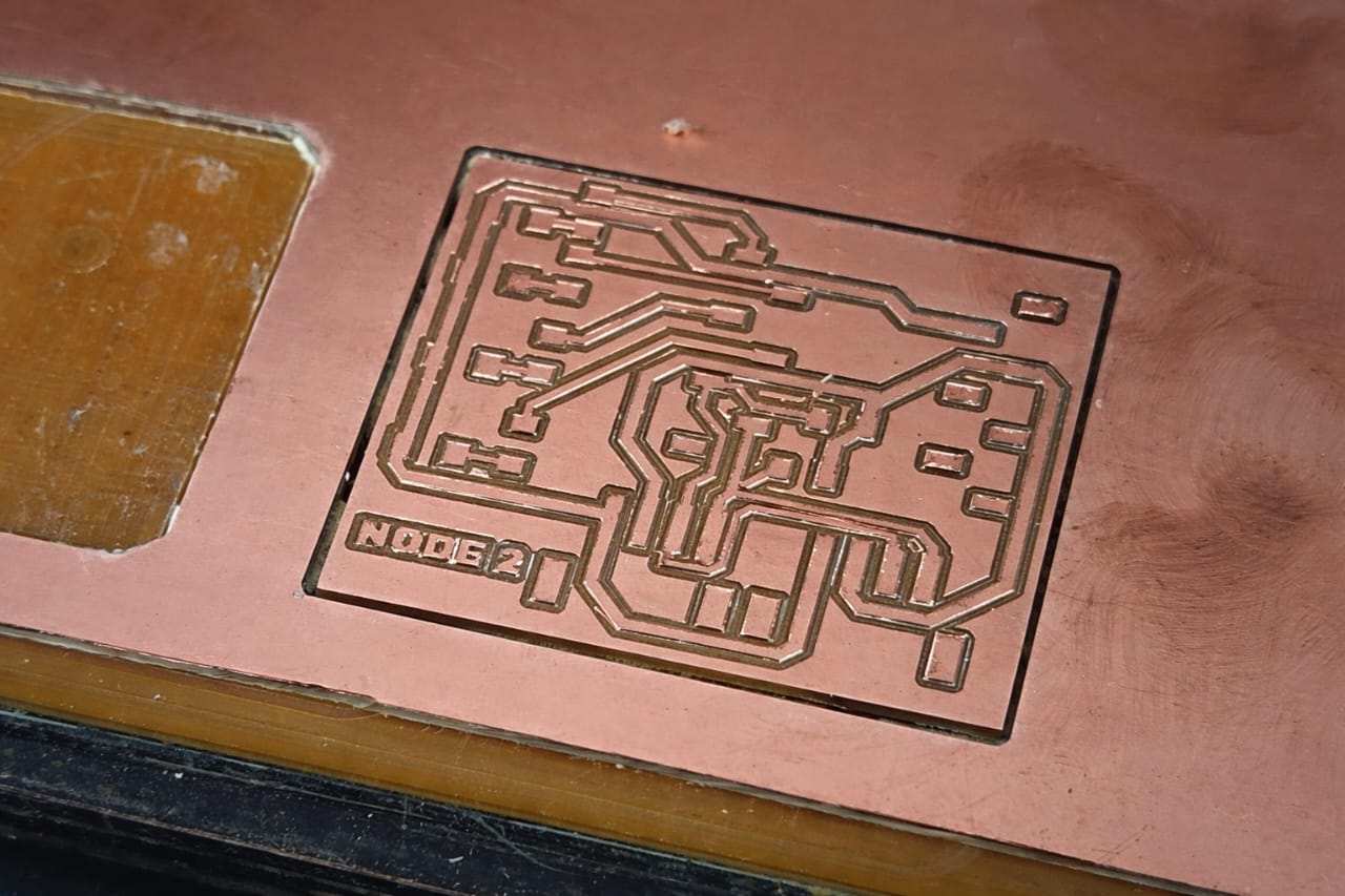
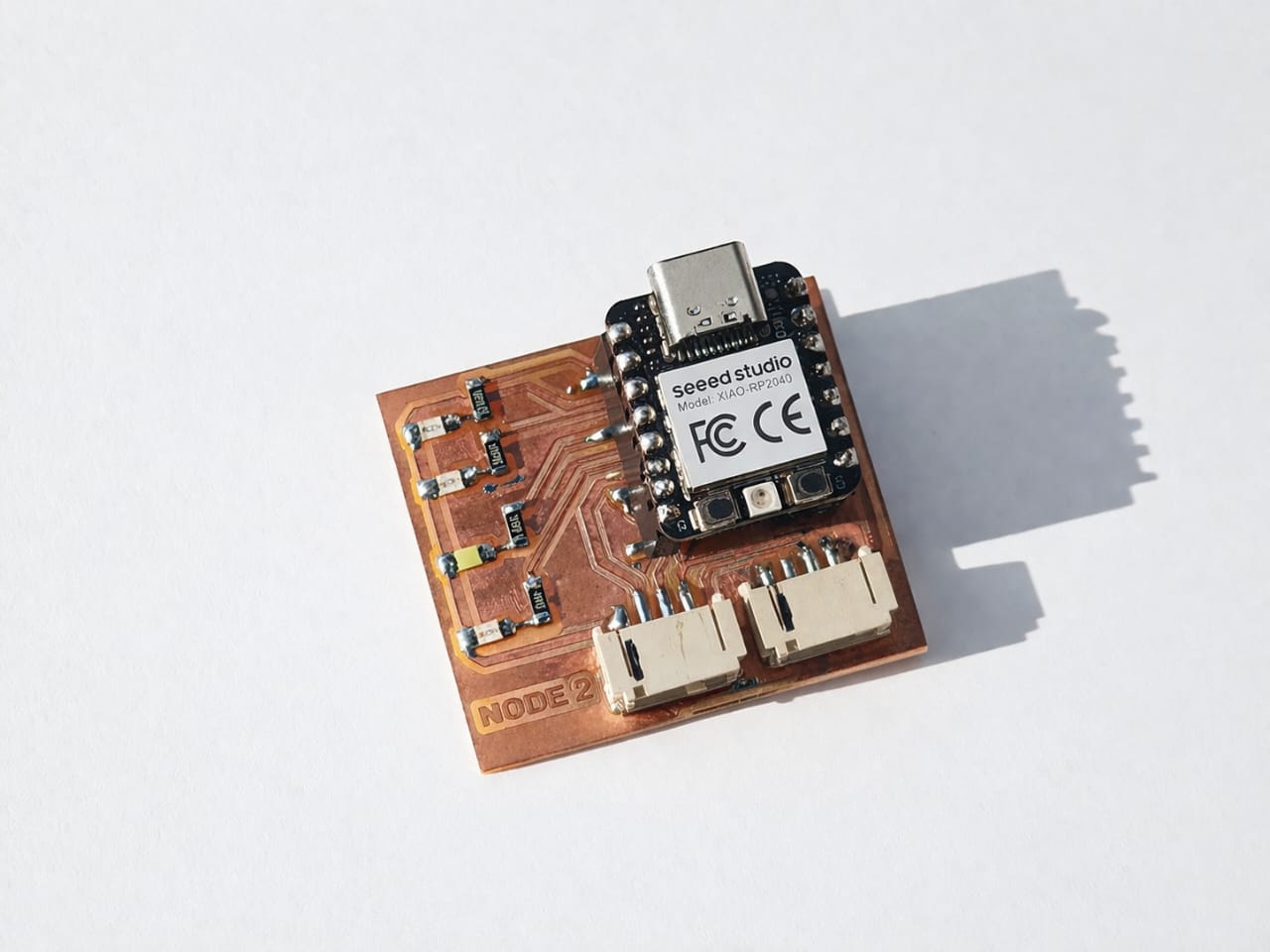
Node 2 – LED PCB (Week 11)
Why 2 nodes
I created Node 2 to demonstrate a true networking system. While connecting just two boards (1 Master and 1 Node) shows simple point-to-point communication, adding a second node (Node 2) proves that the Master can successfully address, manage, and coordinate multiple independent devices on the same I2C network line.
For this week, I designed and fabricated a new PCB with 4 SMD LEDs. This board acts as another I2C NODE device.
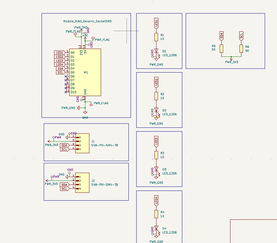
Once complete, we transfer the schematic to the PCB Editor using the "Update PCB from Schematic" tool. In the PCB Editor, drew the board outline on the Edge.Cuts layer. Then route the copper traces using the Route Tracks tool. Finally, a Design Rule Check (DRC) helps ensure there are no layout violations. After verifying the design, we can generate Gerber files for fabrication.
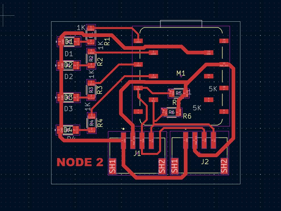
I used Gerber2png software to convert my PCB design's Gerber files into PNG images. After the conversion, I obtained separate images for the trace layer and the outline layer. The trace layer showed the copper connections on the board, illustrating how the components were electrically linked. The outline layer displayed the board's physical boundary, which I had drawn on the Edge.Cuts layer in KiCad.
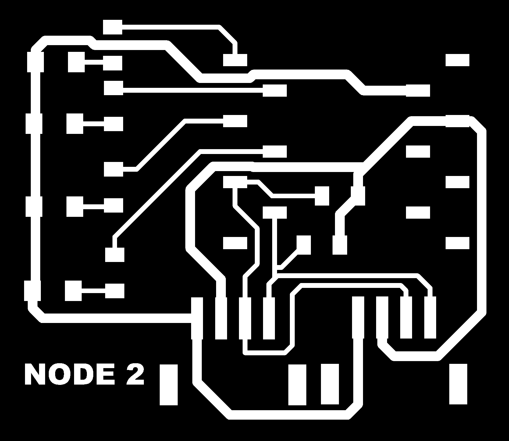

I then uploaded the trace and outline images into mods CE, setting them up for PCB milling.
Milling the PCB
I used mods CE and a Roland Modela MDX-20 milling machine to fabricate the new PCB. The setup, trace milling with a 1/64-inch bit, and outline cutting with a 1/32-inch bit follow the exact same workflow detailed in my Week 08 assignment.
Assembling the Components
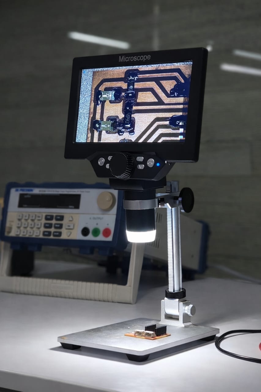
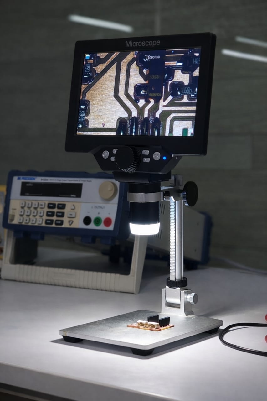
I used the Interactive HTML BOM to identify and source the components from FabStash. After soldering the parts onto the PCB, I verified the quality using two methods:
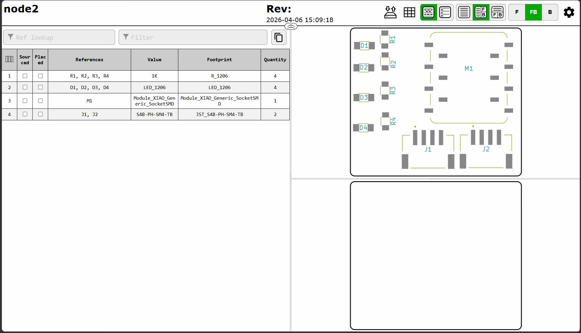
Inspecting the PCBs
- Visual Inspection: Checked under a microscope for solder bridges, component alignment, and cold joints.
- Electrical Testing: Used a multimeter to verify continuity and ensure proper connections.
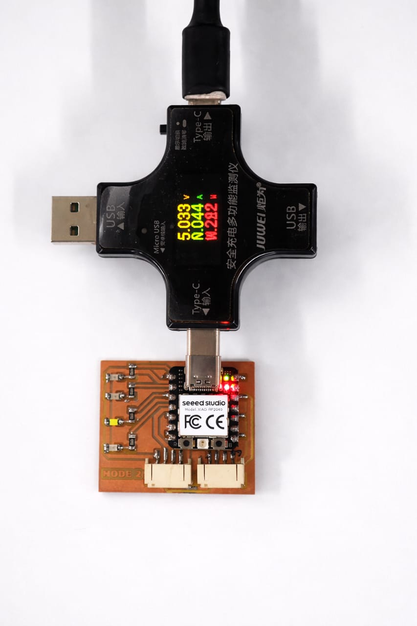
Node 2 Image
Node 2 Code
#include <Wire.h>

#define SLAVE_ADDRESS 0x09
#define LED_PIN 3

void setup() {
  pinMode(LED_PIN, OUTPUT);
  Wire.begin(SLAVE_ADDRESS);
  Wire.onReceive(receiveEvent);
}

void loop() {}

void receiveEvent(int x) {
  int cmd = Wire.read();

  if(cmd == 1){
    digitalWrite(LED_PIN, HIGH);
    delay(500);
    digitalWrite(LED_PIN, LOW);
  }
}
Node 2 Working Video
Final Communication (All Boards)
Master and Node 1 Communication (OLED & Motor)
The master board sends data to Node 1 through I2C communication. Node 1 displays information on the OLED and activates the vibrating motor based on received signals.
Master Code
#include <Wire.h>

#define SDA_PIN D4
#define SCL_PIN D5
#define MOTOR_PIN D2

volatile int mode = 0;

void receiveEvent(int howMany) {
  while (Wire.available()) {
    mode = Wire.read();
  }
}

void setup() {
  pinMode(MOTOR_PIN, OUTPUT);

  Wire.setSDA(SDA_PIN);
  Wire.setSCL(SCL_PIN);
  Wire.begin(8);

  Wire.onReceive(receiveEvent);
}

void loop() {

  if (mode == 0) {
    digitalWrite(MOTOR_PIN, LOW);
  }

  else if (mode == 1) {
    digitalWrite(MOTOR_PIN, HIGH);
    delay(100);
    digitalWrite(MOTOR_PIN, LOW);
    delay(100);
  }

  else if (mode == 2) {
    digitalWrite(MOTOR_PIN, HIGH);
    delay(50);
    digitalWrite(MOTOR_PIN, LOW);
    delay(50);
  }

  else if (mode == 3) {
    digitalWrite(MOTOR_PIN, HIGH);
  }
}
Node 1 Code
#include <Wire.h>

// USE GPIO NUMBERS (NOT D PINS)
#define SDA_PIN 4
#define SCL_PIN 5
#define MOTOR_PIN 2   // MOSFET control pin

volatile int mode = 0;

// I2C receive function
void receiveEvent(int howMany) {
  while (Wire.available()) {
    mode = Wire.read();
  }
}

void setup() {
  pinMode(MOTOR_PIN, OUTPUT);
  analogWrite(MOTOR_PIN, 0); // motor OFF initially

  // I2C SLAVE INIT
  Wire.setSDA(SDA_PIN);
  Wire.setSCL(SCL_PIN);
  Wire.begin(8);   // slave address = 8

  Wire.onReceive(receiveEvent);
}

void loop() {

  // Motor vibration control
  switch (mode) {

    case 0: // OFF
      analogWrite(MOTOR_PIN, 0);
      break;

    case 1: // LOW vibration
      analogWrite(MOTOR_PIN, 80);
      break;

    case 2: // MEDIUM vibration
      analogWrite(MOTOR_PIN, 150);
      break;

    case 3: // HIGH vibration
      analogWrite(MOTOR_PIN, 255);
      break;

    default:
      analogWrite(MOTOR_PIN, 0);
      break;
  }

  delay(5); // stability
}
Working Video
Final I2C Communication Setup
All boards were connected together using I2C communication with shared SDA and SCL lines. The master successfully controlled both Node 1 and Node 2 simultaneously.
Master Code
#include <Wire.h>
#include <Adafruit_GFX.h>
#include <Adafruit_SSD1306.h>

#define SCREEN_WIDTH 128
#define SCREEN_HEIGHT 32

#define SDA_PIN D4
#define SCL_PIN D5
#define BUTTON_PIN D3

Adafruit_SSD1306 display(SCREEN_WIDTH, SCREEN_HEIGHT, &Wire, -1);

int mode = 0;
int lastButtonState = HIGH;
unsigned long lastDebounceTime = 0;
int debounceDelay = 200;

void showDisplay() {
  display.clearDisplay();
  display.setCursor(0, 10);

  display.print("MODE: ");

  switch (mode) {
    case 0: display.println("OFF"); break;
    case 1: display.println("LOW"); break;
    case 2: display.println("MED"); break;
    case 3: display.println("HIGH"); break;
  }

  display.display();
}

void setup() {

  pinMode(BUTTON_PIN, INPUT_PULLUP);

  Wire.setSDA(SDA_PIN);
  Wire.setSCL(SCL_PIN);
  Wire.begin();   // MASTER

  if (!display.begin(SSD1306_SWITCHCAPVCC, 0x3C)) {
    while (1);
  }

  display.setTextSize(1);
  display.setTextColor(WHITE);

  showDisplay();
}

void loop() {

  int reading = digitalRead(BUTTON_PIN);

  if (reading == LOW && lastButtonState == HIGH &&
      (millis() - lastDebounceTime) > debounceDelay) {

    lastDebounceTime = millis();

    mode++;
    if (mode > 3) mode = 0;

    showDisplay();

    // Send to Slave 1
    Wire.beginTransmission(8);
    Wire.write(mode);
    Wire.endTransmission();

    // Send to Slave 2
    Wire.beginTransmission(9);
    Wire.write(mode);
    Wire.endTransmission();
  }

  lastButtonState = reading;
}
Node 1 Code
#include <Wire.h>
#include <Adafruit_GFX.h>
#include <Adafruit_SSD1306.h>

#define SCREEN_WIDTH 128
#define SCREEN_HEIGHT 32

#define SDA_PIN D4
#define SCL_PIN D5
#define MOTOR_PIN D2

Adafruit_SSD1306 display(SCREEN_WIDTH, SCREEN_HEIGHT, &Wire, -1);

volatile int mode = 0;

void receiveEvent(int howMany) {
  while (Wire.available()) {
    mode = Wire.read();
  }
}

void setup() {

  pinMode(MOTOR_PIN, OUTPUT);
  analogWrite(MOTOR_PIN, 0);

  Wire.setSDA(SDA_PIN);
  Wire.setSCL(SCL_PIN);
  Wire.begin(8);   // SLAVE 1
  Wire.onReceive(receiveEvent);

  if (!display.begin(SSD1306_SWITCHCAPVCC, 0x3C)) {
    while (1);
  }

  display.setTextSize(1);
  display.setTextColor(WHITE);
}

void loop() {

  display.clearDisplay();
  display.setCursor(0, 10);

  display.print("MODE: ");

  switch (mode) {

    case 0:
      display.println("OFF");
      analogWrite(MOTOR_PIN, 0);
      break;

    case 1:
      display.println("LOW");
      analogWrite(MOTOR_PIN, 80);
      break;

    case 2:
      display.println("MED");
      analogWrite(MOTOR_PIN, 150);
      break;

    case 3:
      display.println("HIGH");
      analogWrite(MOTOR_PIN, 255);
      break;
  }

  display.display();
  delay(50);
}
Node 2 Code
#include <Wire.h>

#define SDA_PIN D4
#define SCL_PIN D5

#define LED1 D0
#define LED2 D1
#define LED3 D2
#define LED4 D3

volatile int mode = 0;

void receiveEvent(int howMany) {
  while (Wire.available()) {
    mode = Wire.read();
  }
}

void setup() {

  pinMode(LED1, OUTPUT);
  pinMode(LED2, OUTPUT);
  pinMode(LED3, OUTPUT);
  pinMode(LED4, OUTPUT);

  Wire.setSDA(SDA_PIN);
  Wire.setSCL(SCL_PIN);
  Wire.begin(9);   // SLAVE 2
  Wire.onReceive(receiveEvent);
}

void loop() {

  digitalWrite(LED1, LOW);
  digitalWrite(LED2, LOW);
  digitalWrite(LED3, LOW);
  digitalWrite(LED4, LOW);

  switch (mode) {

    case 1:
      digitalWrite(LED1, HIGH);
      break;

    case 2:
      digitalWrite(LED2, HIGH);
      digitalWrite(LED3, HIGH);
      break;

    case 3:
      digitalWrite(LED1, HIGH);
      digitalWrite(LED2, HIGH);
      digitalWrite(LED3, HIGH);
      digitalWrite(LED4, HIGH);
      break;
  }

  delay(10);
}
AI code Prompt
chat gpt prompt: i want eo turn on master node1 and node2 when i press botton in master 3 modes light in blink led in master then vibrate in node2 and show in oled and blink led in node2 in 3mode give code"
AI Tool Used: ChatGPT
Final Working Video
I2C Communication Test
To verify communication between nodes, an I2C scanner was used.
The scanner detected a device at address 0x08, confirming that Slave 1 is properly connected and communicating with the master.
Further debugging showed that the second slave address 0x09 was also detected after corrections were made.
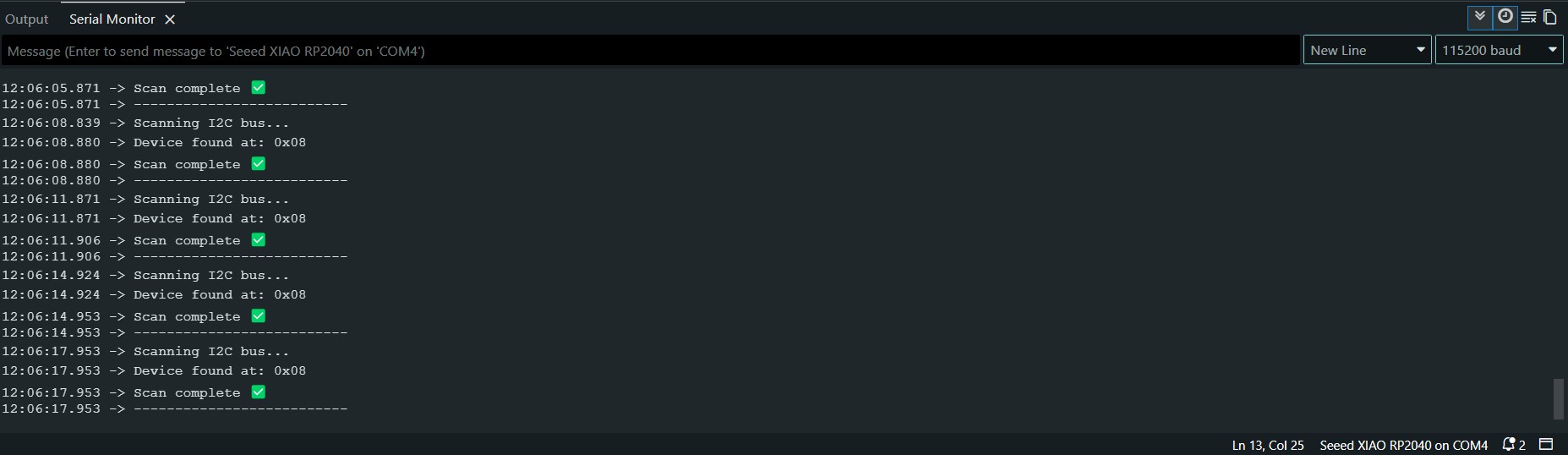
Figure: I2C scanner output showing detected device at address 0x08.
I2C Addressing and Communication
1. Node Addressing
node is assigned its own unique address
Wire.begin(8); // node 1
node 2
Wire.begin(9); // node 2
both node have Wire.onReceive(receiveEvent);
Master Control
When the control button is pressed, the Master sends the updated data to each node one after the other by calling their exact address:
Sending to Node 1:
Wire.beginTransmission(8); // Targets Node 1 specifically
Wire.write(mode);          // Sends the current mode value
Wire.endTransmission();    // Completes the transfer
Sending to Node 2:
Wire.beginTransmission(9); // Targets Node 2 specifically
Wire.write(mode);          // Sends the exact same mode value
Wire.endTransmission();    // Completes the transfer
Conclusion
In this week, I successfully implemented communication between multiple PCBs using the I2C protocol. I connected one master board and two slave boards, assigned unique addresses, and verified communication. This helped me understand networking between embedded devices.
Hero Shot
Problems and Fixes
During the programming and testing phase, Node 2 was failing to communicate on the I2C network.
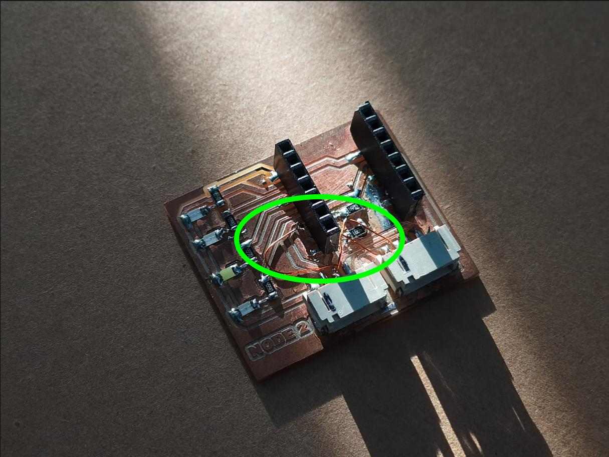
Figure: The area on Node 2 where the swapped SCL and SDA traces were corrected using enamel wire.
The Issue & Resolution:
- Problem: The SCL (Serial Clock) and SDA (Serial Data) lines were accidentally swapped in the PCB layout design, which prevented the I2C communication from establishing.
- Fix: With guidance from my instructor, Saheen, I carefully cut the incorrect copper traces on the board using a hobby knife. I then used thin enamel copper wire to cross and resolder the lines to their correct pins, restoring proper I2C communication.
Group Assignment
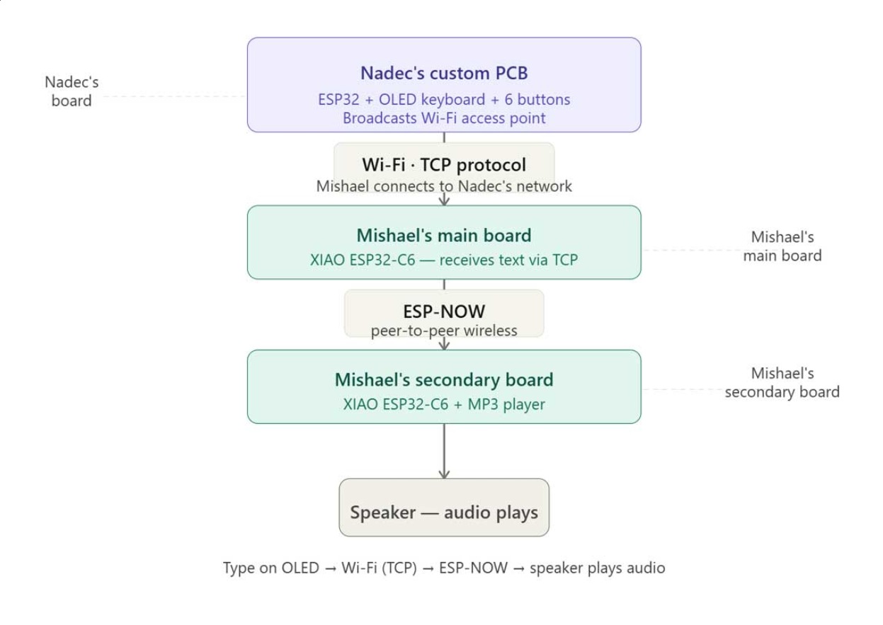
For group assigement communicate with different person project wired or wireless.here we takes the text typed on Nadec's device is sent wirelessly through Mishael's main and secondary boards to finally play as audio through a speaker.
This week was guided by Saheen and Ashish.
Group Assignment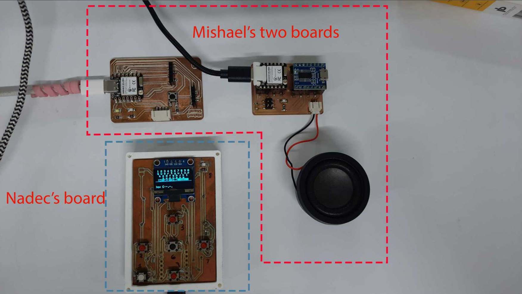
this is communication flow chart