Week 08.Electronics Production
Objectives
Group assignment
Individual assignment:
Group Assignment
PCB fabrication involves design validation, layer etching, drilling, plating, solder masking, and final profiling. Using the Roland MDX-20 milling machine, PCB traces are precisely cut, with minimum trace spacing of ≥17 mils and widths of ≥10 mils for reliability. Alternatively, the XTool F1 Ultra laser engraver offers a faster, non-contact approach by vaporizing copper to form traces, but challenges like overburning and limited depth control affect precision. Testing with a Trotec laser cutter showed poor results due to inconsistent engraving. While milling remains reliable, laser engraving shows potential with further optimization for fine detail and consistency.
To know more, visitGroup Assignment.
PCB PRODUCTION
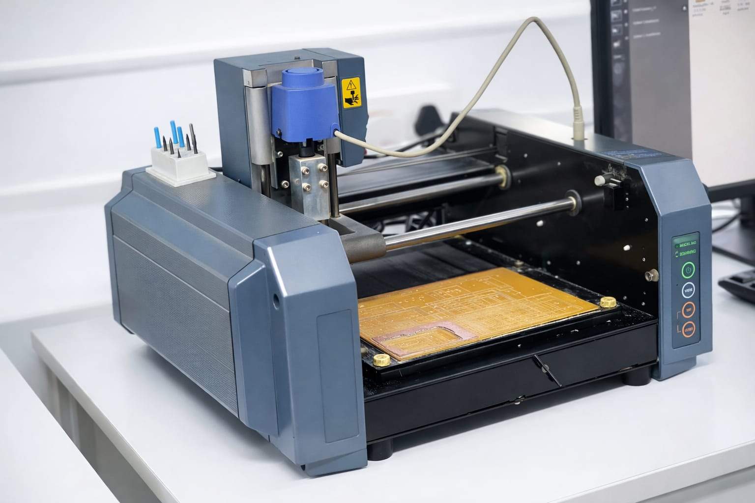
The Roland Modela MDX. is a compact and highly versatile desktop milling machine developed by Roland DG Corporation. Designed for precision milling, carving, and engraving, it is capable of working with a range of materials, including plastic, wood, resin, and non-ferrous metals. With its ability to produce fine details, the MDX-20 is widely used in prototyping, model making, jewelry design, and small-scale manufacturing.
Design
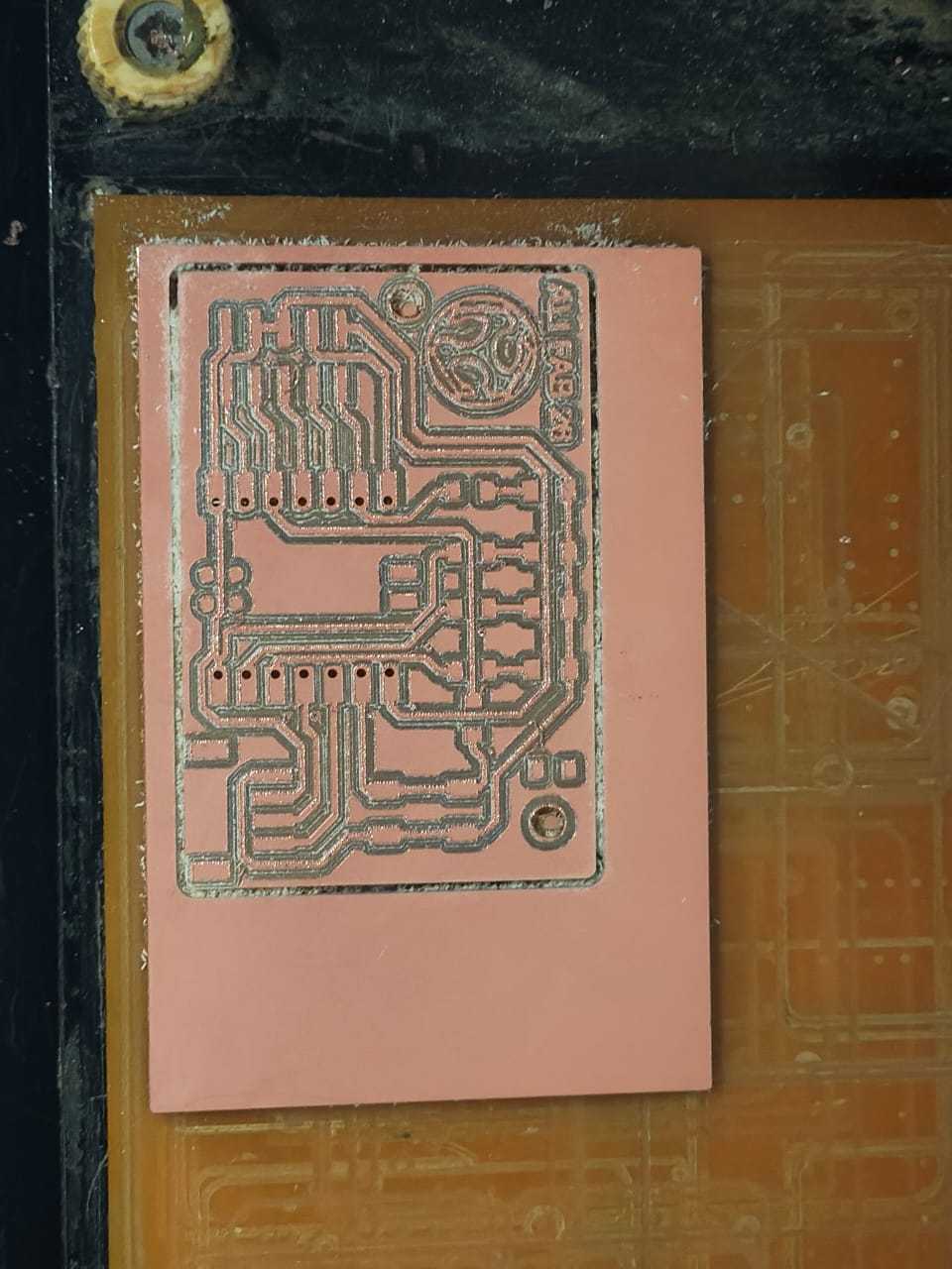
I would be making the space invader PCB that i designed during Week04 where we did electronics designing. I cross verified the board and checked the dimensions of the design which turned out to be 54.31 x 36.71mm.
Gerber files
Gerber to png. files are the standard file format used in the PCB industry to communicate design data from designers to manufacturers. They contain precise instructions for fabricating a PCB, specifying the layout of copper traces, pads, vias, solder masks, silkscreen markings, and drill holes. Each PCB layer is represented by a separate Gerber file, and the format uses ASCII-based vector commands to define shapes and positions. Generated by PCB design software such as KiCad, Altium, or Eagle, these files guide manufacturing processes like CNC milling, photoplotting, and etching.
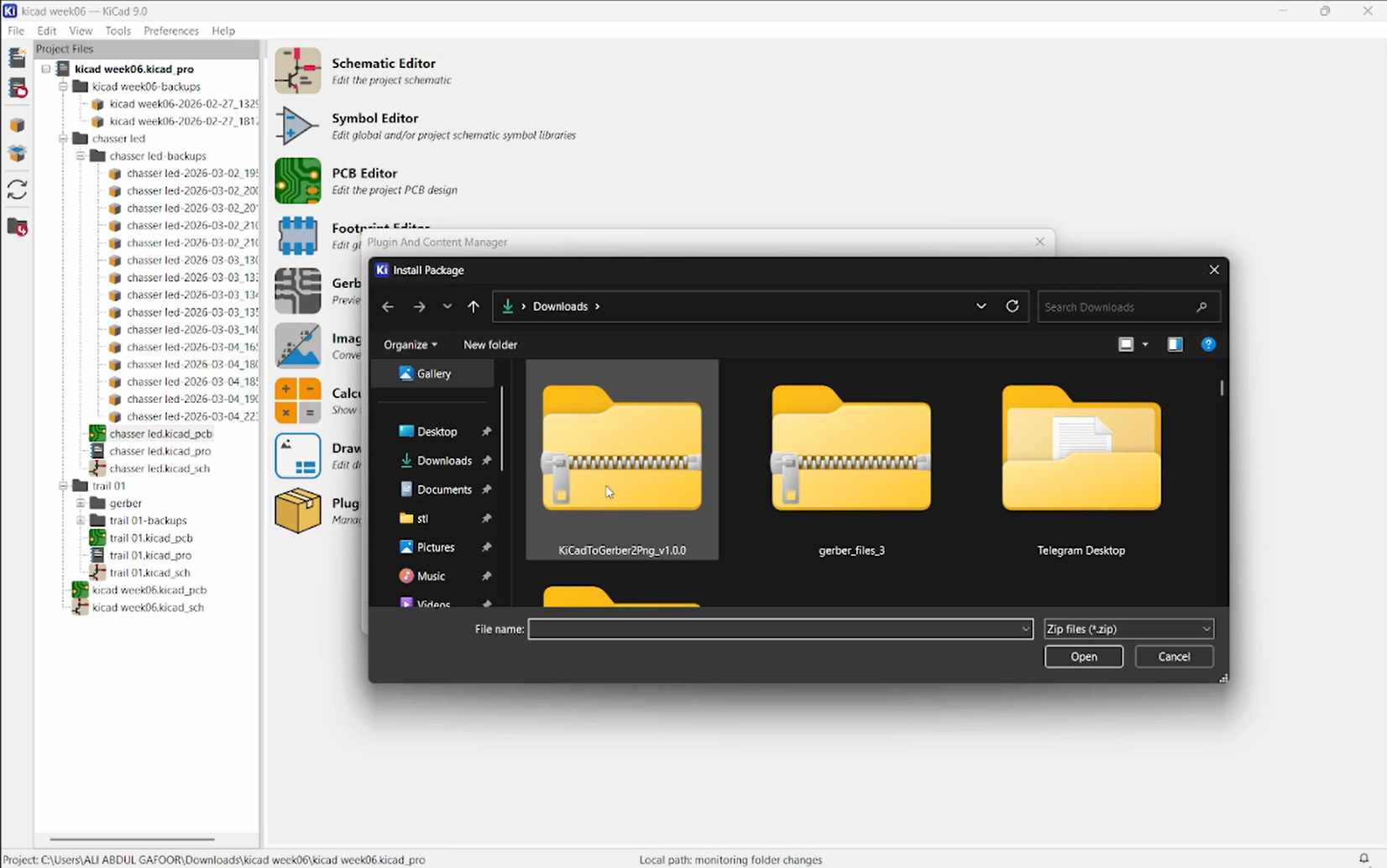
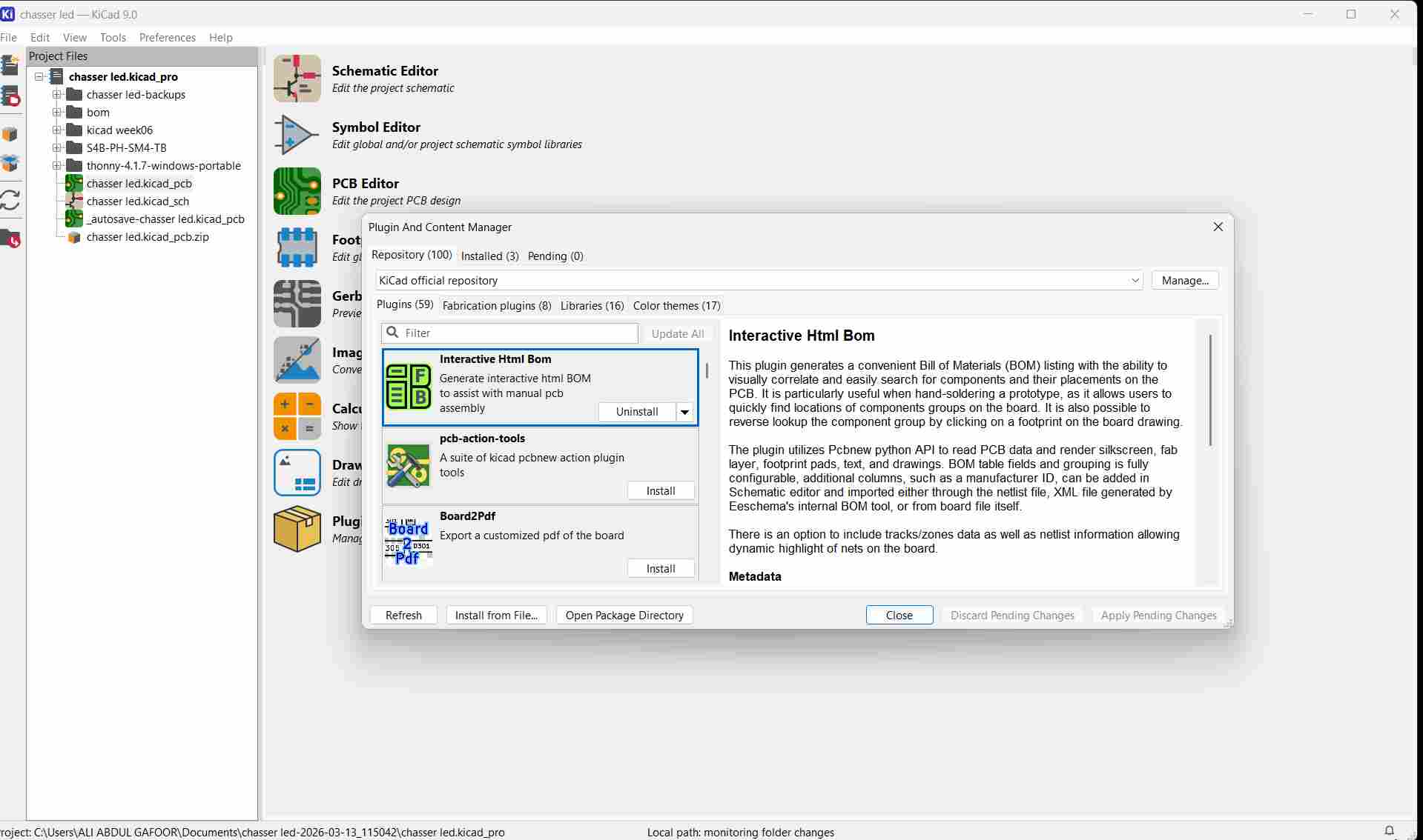
The Gerber to PNG plugin was downloaded from the FabLab Kerala GitHub repository using the HTTPS link.
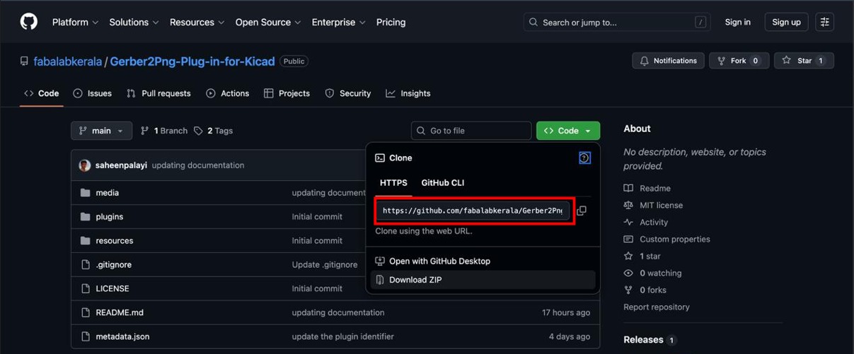
The Gerber to PNG plugin was installed in KiCad using the Plugin and Content Manager by selecting the downloaded ZIP package
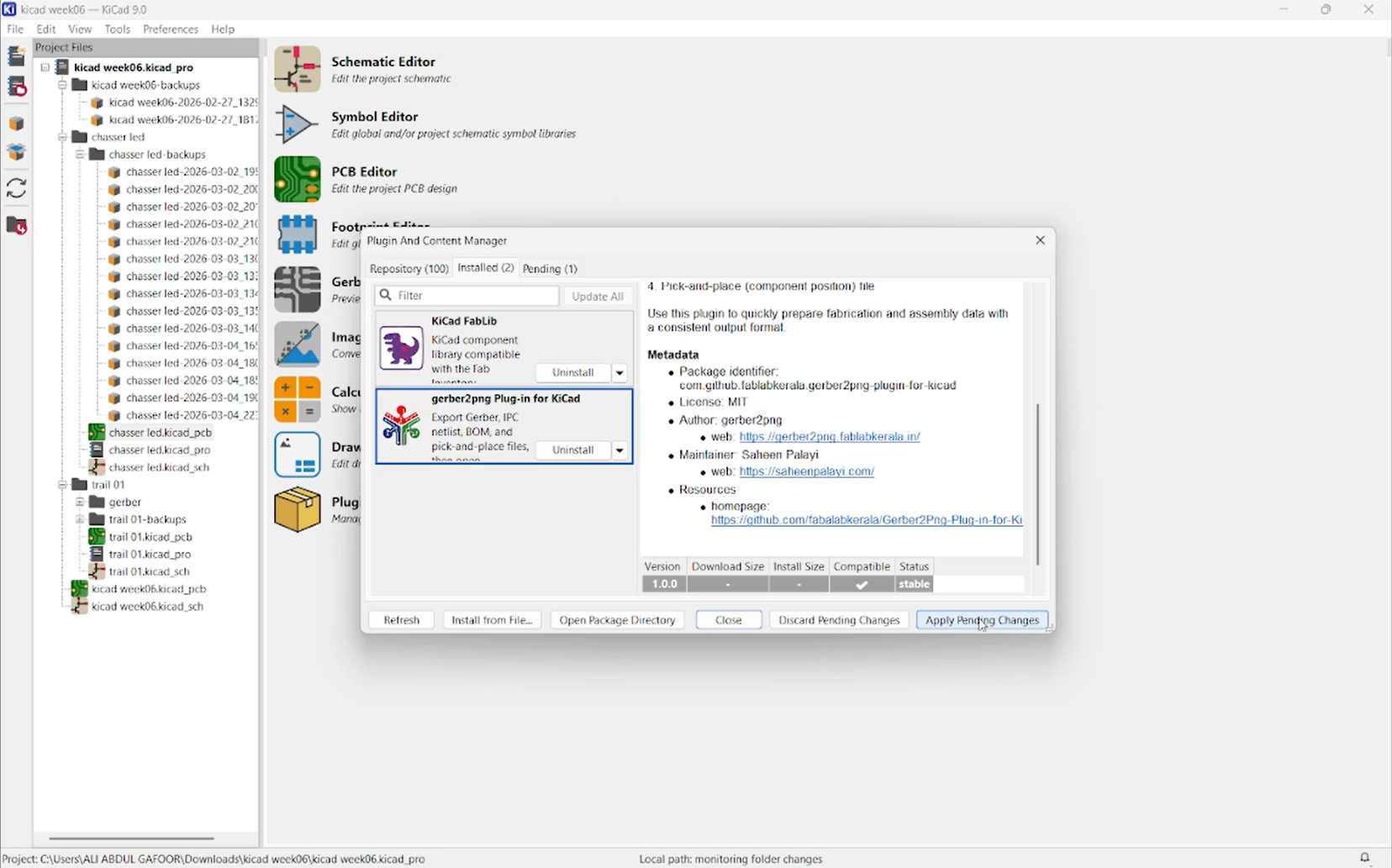
The Gerber2PNG plugin was successfully installed and verified within KiCad's Plugin and Content Manager, confirming readiness for use.
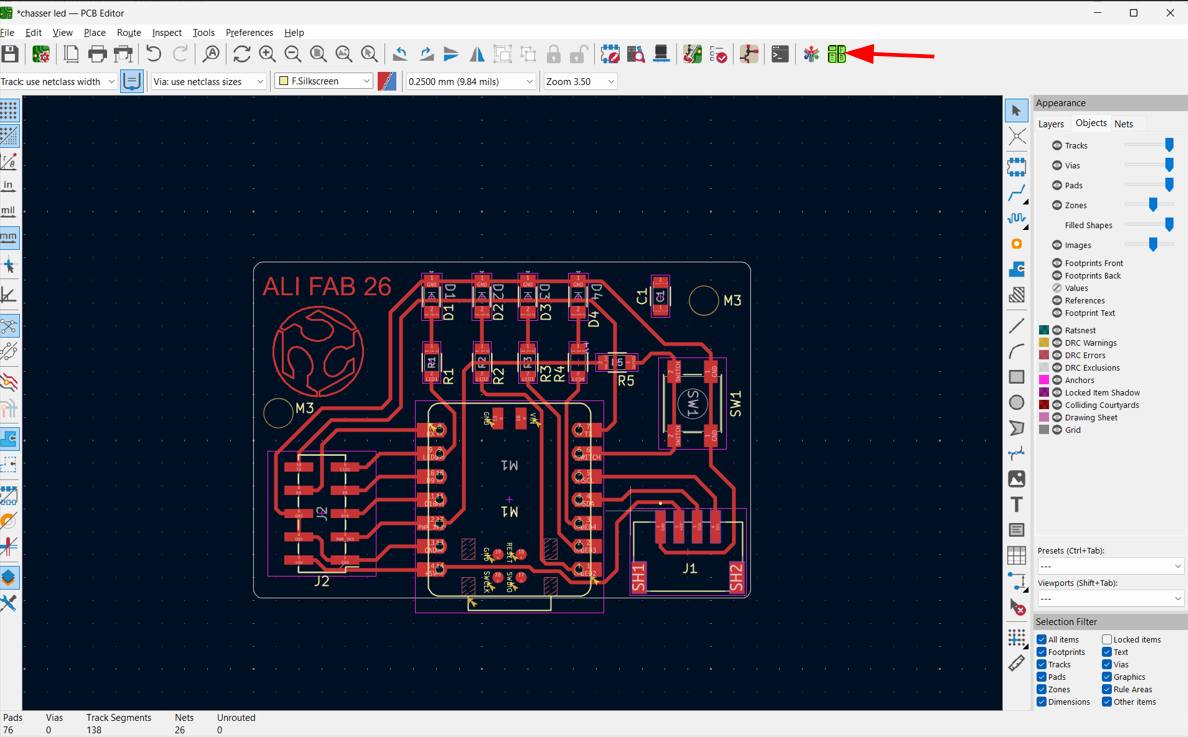
the icon you marked in the KiCad PCB Editor is a Gerber → PNG export tool, and it is a custom plugin developed by FabLab Kerala.
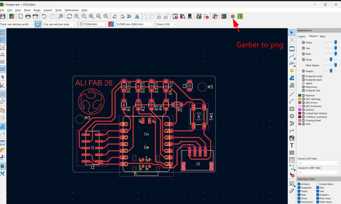
click the Gerber → PNG icon (FabLab Kerala plugin) it automatically generates 3 PNG images for different machining operations of the PCB.
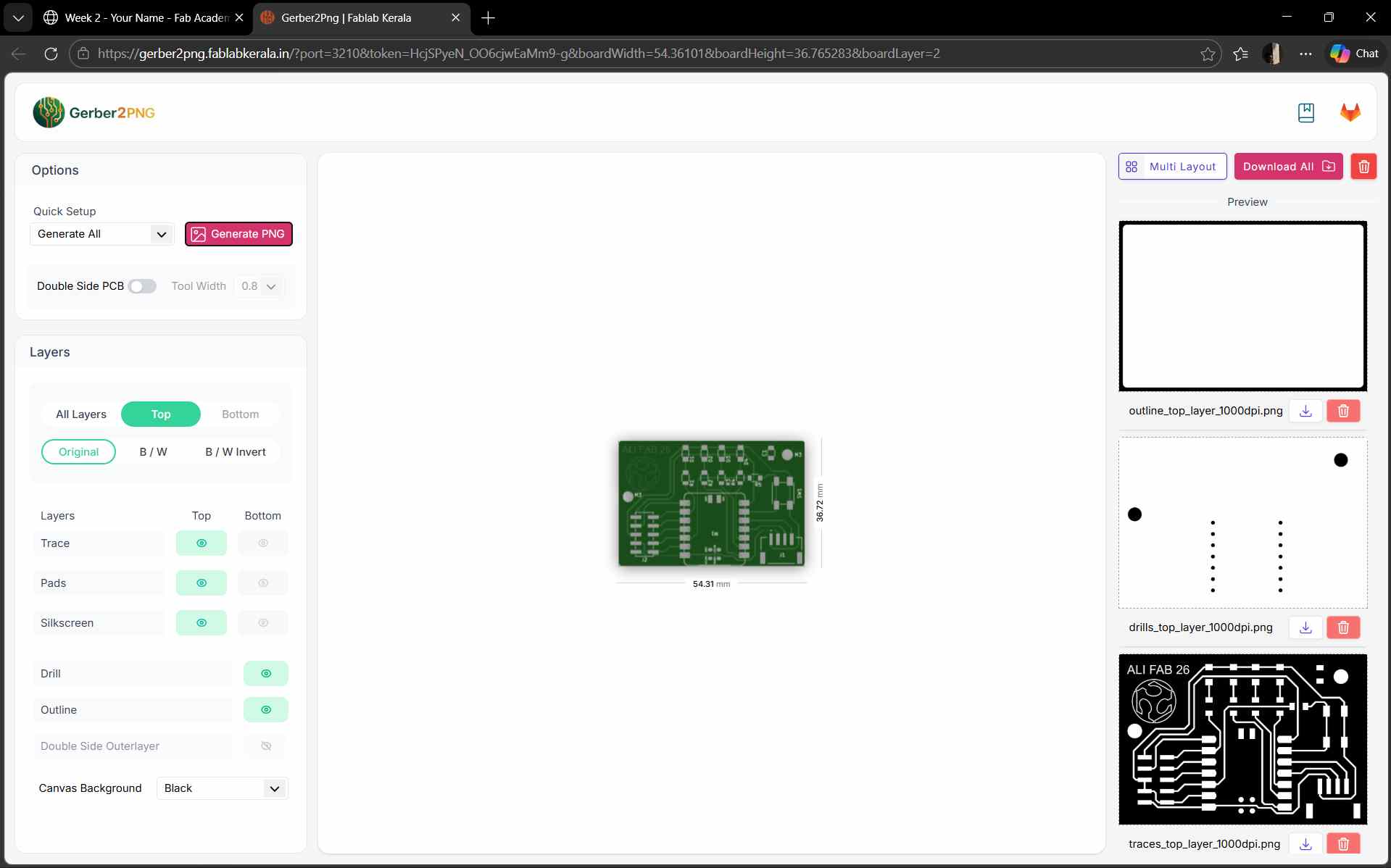
This PNG contains only the PCB traces (copper paths).
.png)
This PNG shows all drill holes.
.png)
This PNG contains the PCB board outline.
.png)
This PNG contains the PCB board outline.
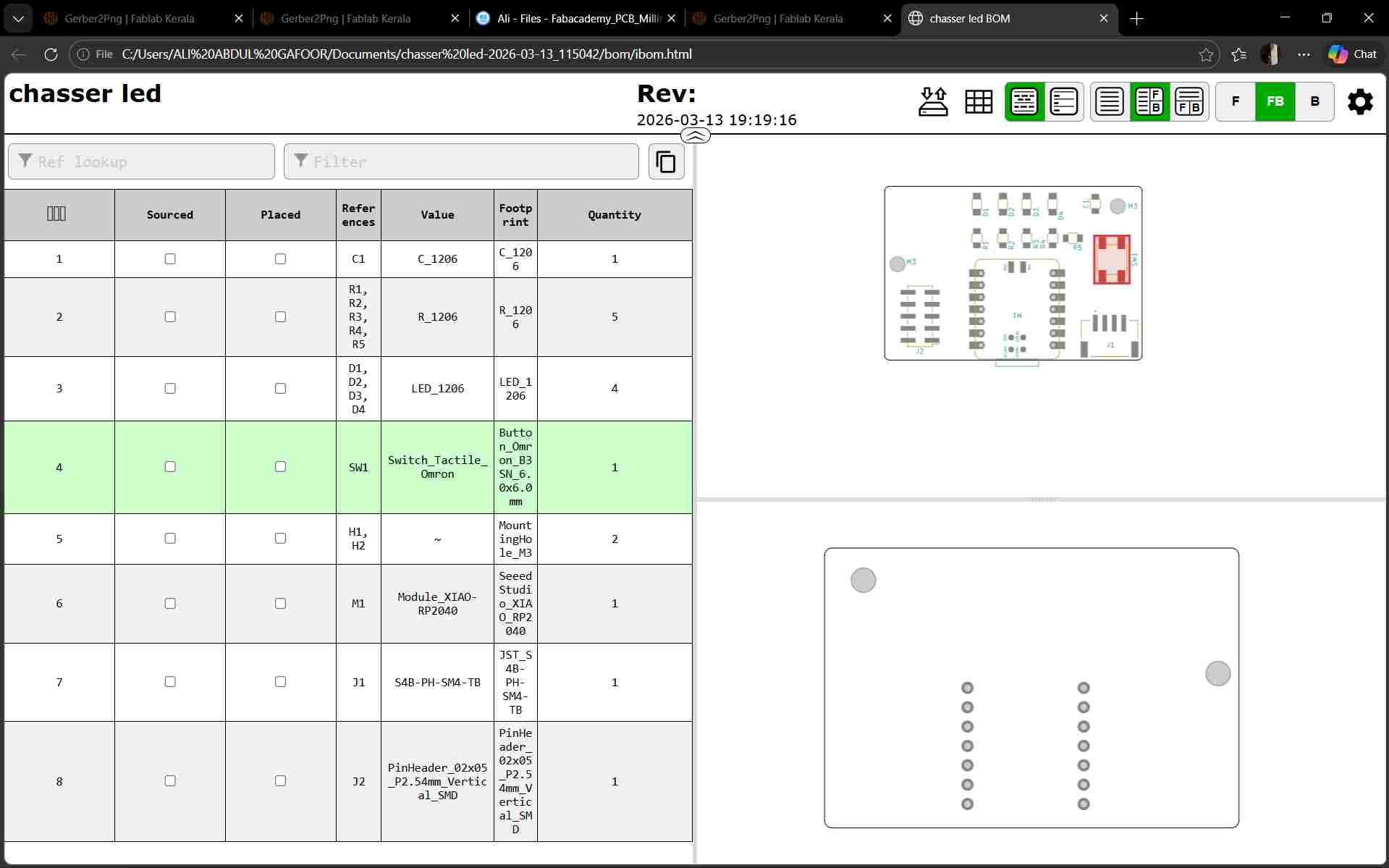
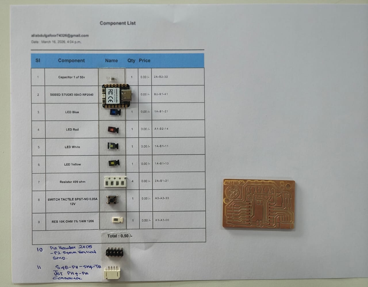
We have to collect the components required for our PCB and prepare a BOM for it.
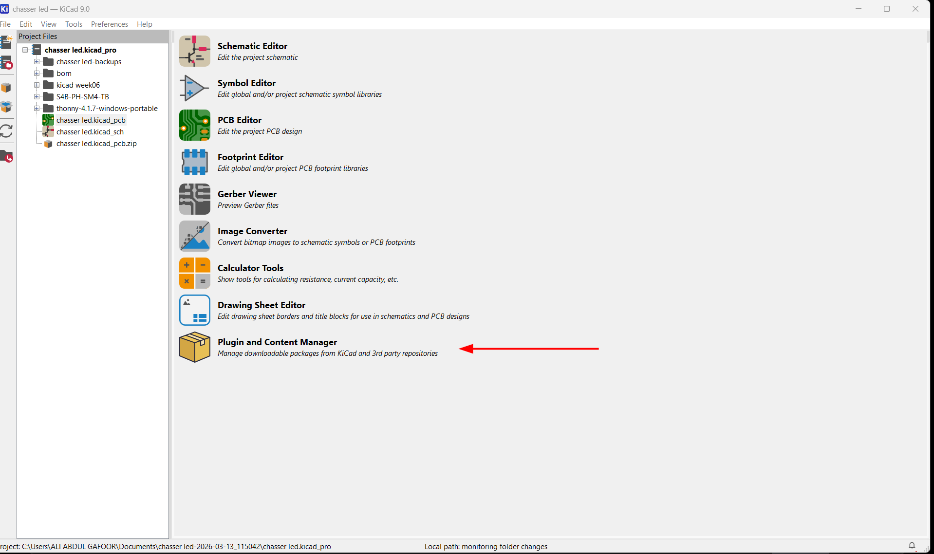
Then install the Interactive Html BOM plugin
this was how the BOM looked like for my PCB.
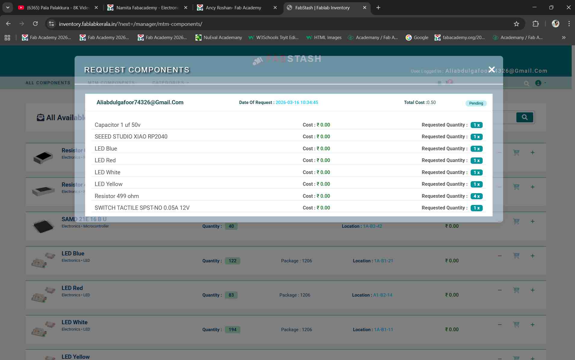
Now we have to check whether all the components that were required is available in our lab's inventory. We were able to check this easily by using Fabstash website which shows the available stock of components in our inventory and keep log of incoming and outgoing items. We can add the parts we need to the cart and send a request to avail them
I printed out the form and went on to pick out the components i required and stuck them on to the paper to easily keep everything in place.
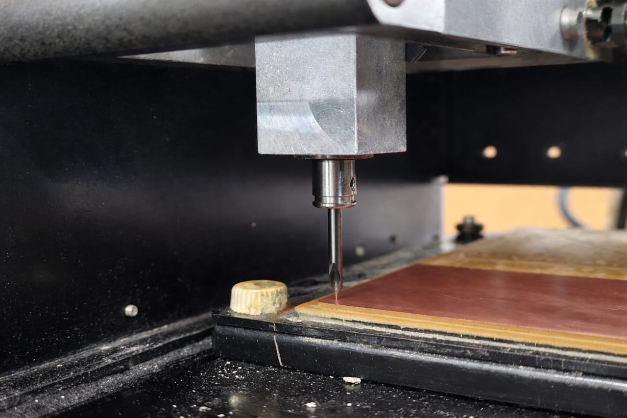
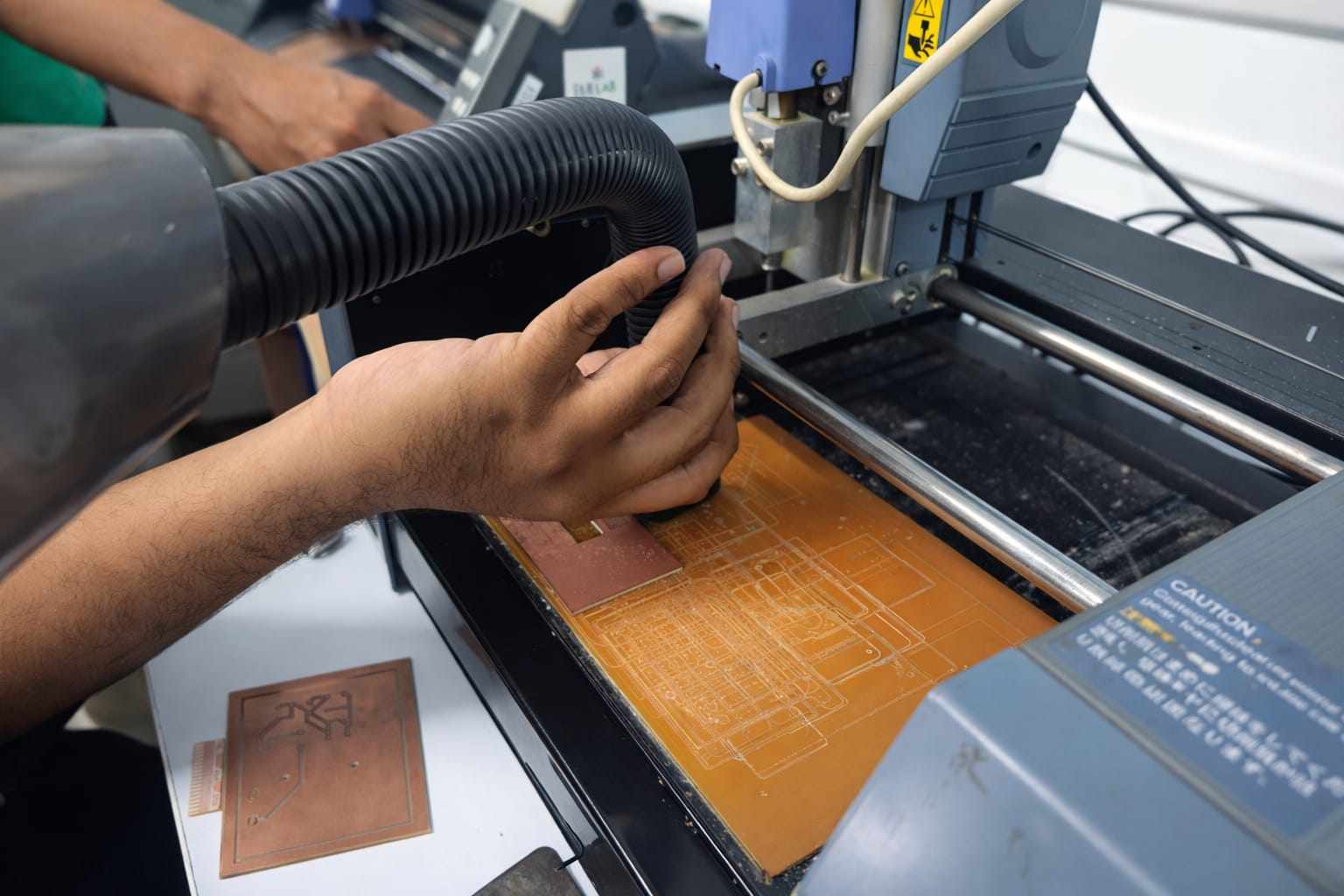
Milling the PCB
Secure the copper-clad board onto the machine's bed using double-sided tape to prevent movement.
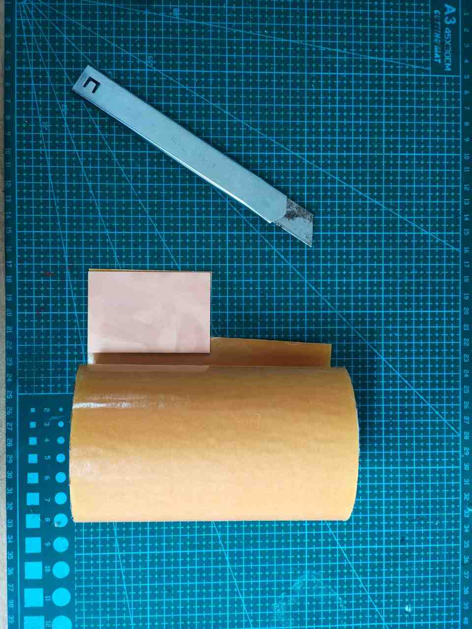
Remove the double-sided sticker and place the PCB in the correct orientation. Confirm there is no deviation and press it properly to stick firmly.
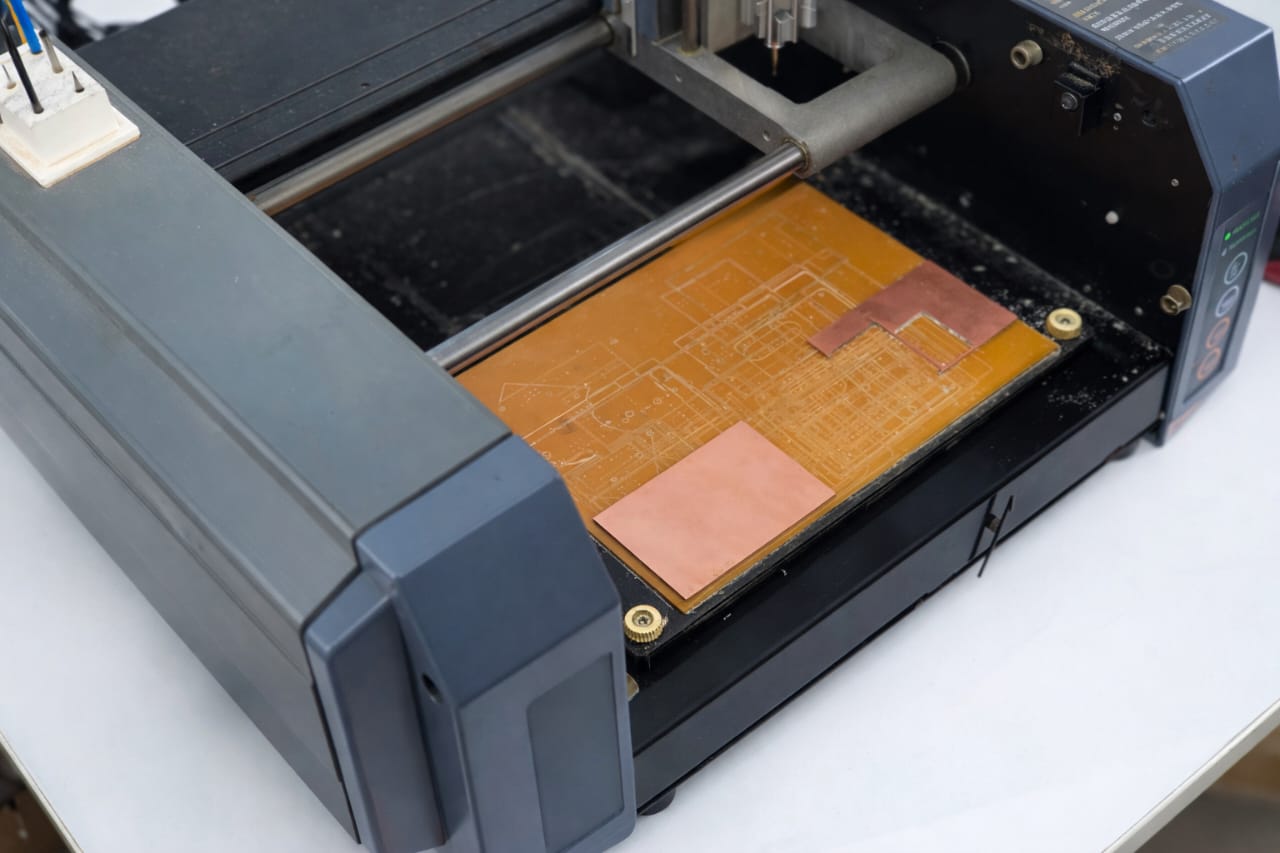
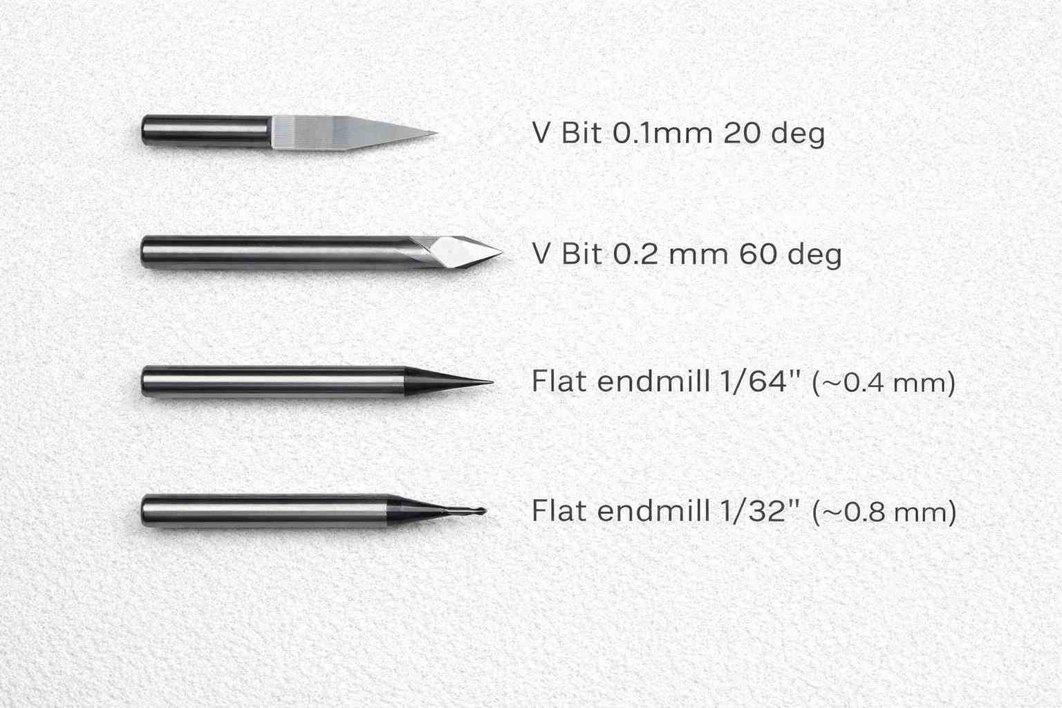
Insert the appropriate engraving or milling bit. I used V Bit 0.2 mm 60 deg for engraving the circuit traces and flat endmill 1/32" for cutting.
mods project. : Mods is a modular, cross-platform software environment originally developed by MIT's Center for Bits and Atoms (CBA) for digital fabrication workflows. It consists of independent but interconnected modules that can be used to create custom toolchains for CAD, CAM, machine control, automation, and sensor input processing. Running in a browser, Mods allows users to design flexible workflows for specific machines and processes, making it a powerful tool for fabrication labs. Mods CE (Community Edition) is an open-source fork that enhances usability and expands features with community support.

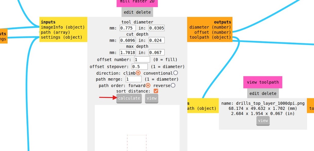
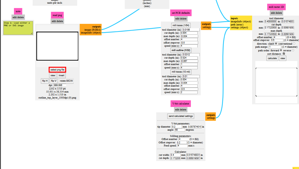
We have to enter a series of commands related to the functioning of the machine. We need the machine to do the traces in the beginning with a 0.2mm 60 degree V bit first , then we go on to do the drilling for the holes and the outlines with a 1/32" flat endmill at the end.
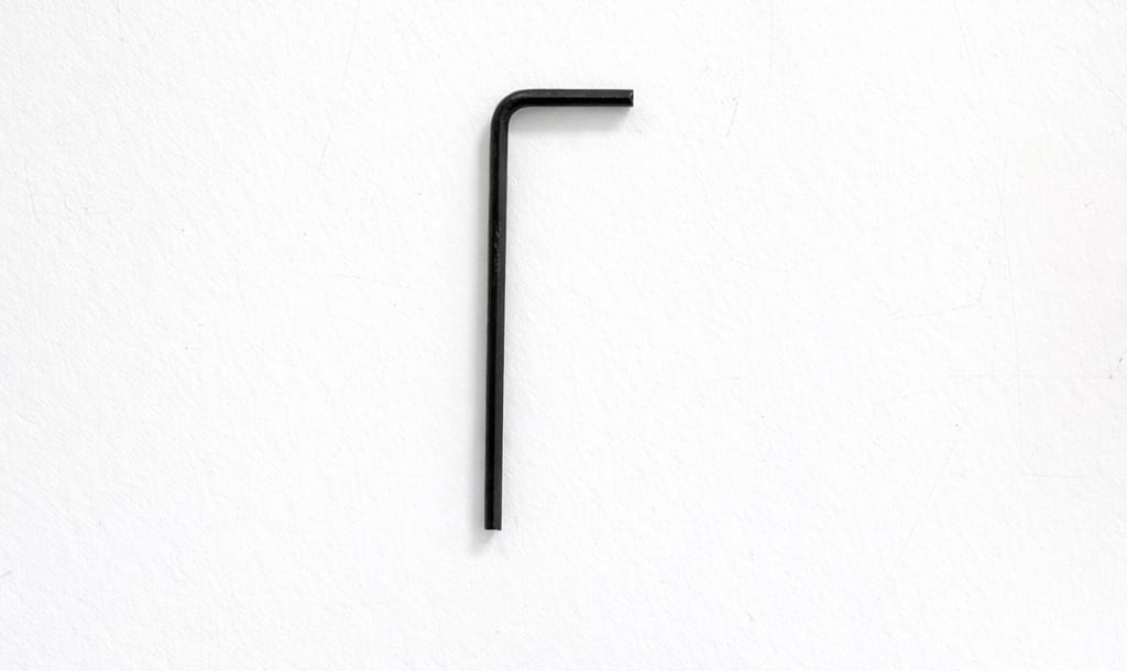
An Allen key is used to tighten and loosen the end mill from the spindle.
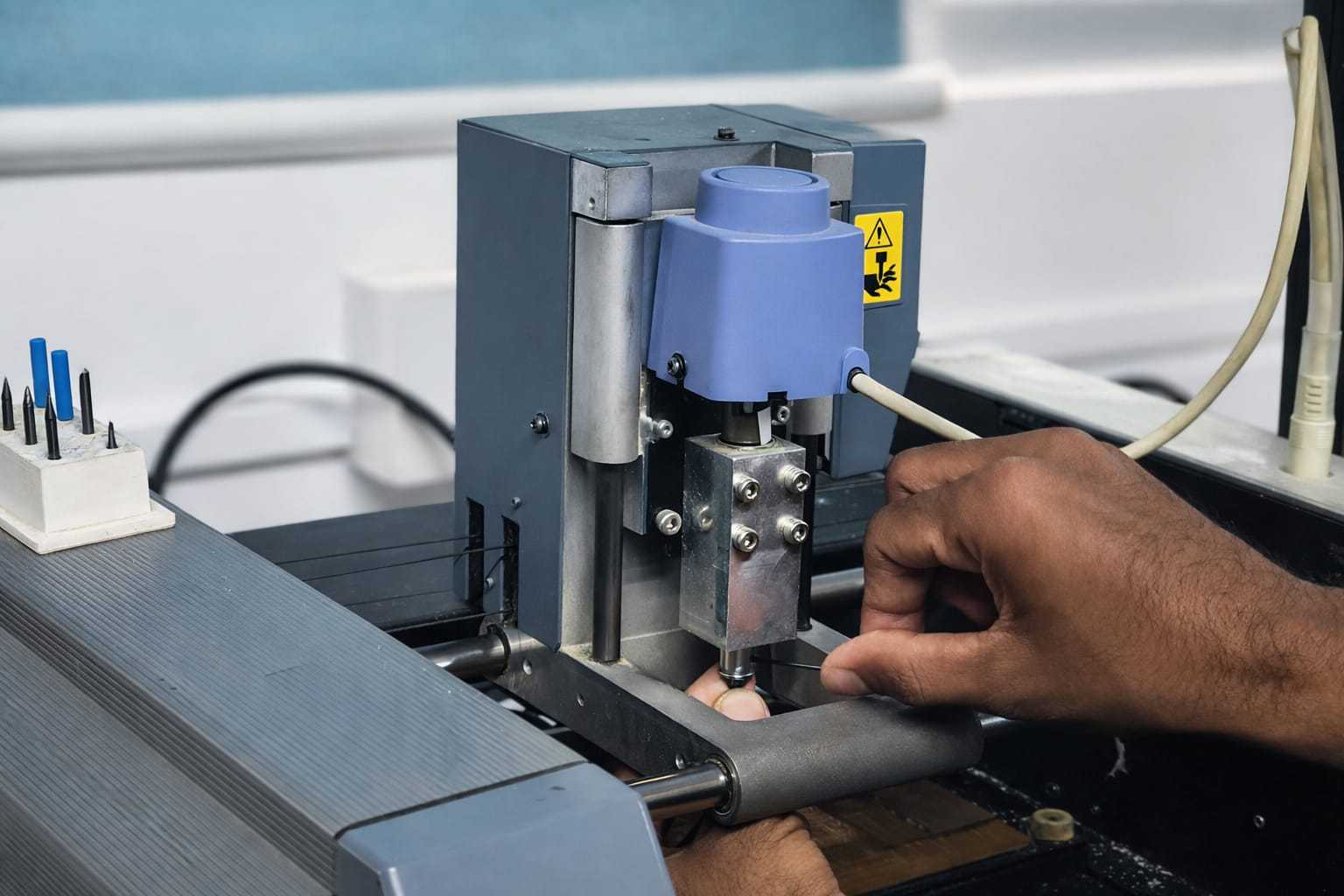
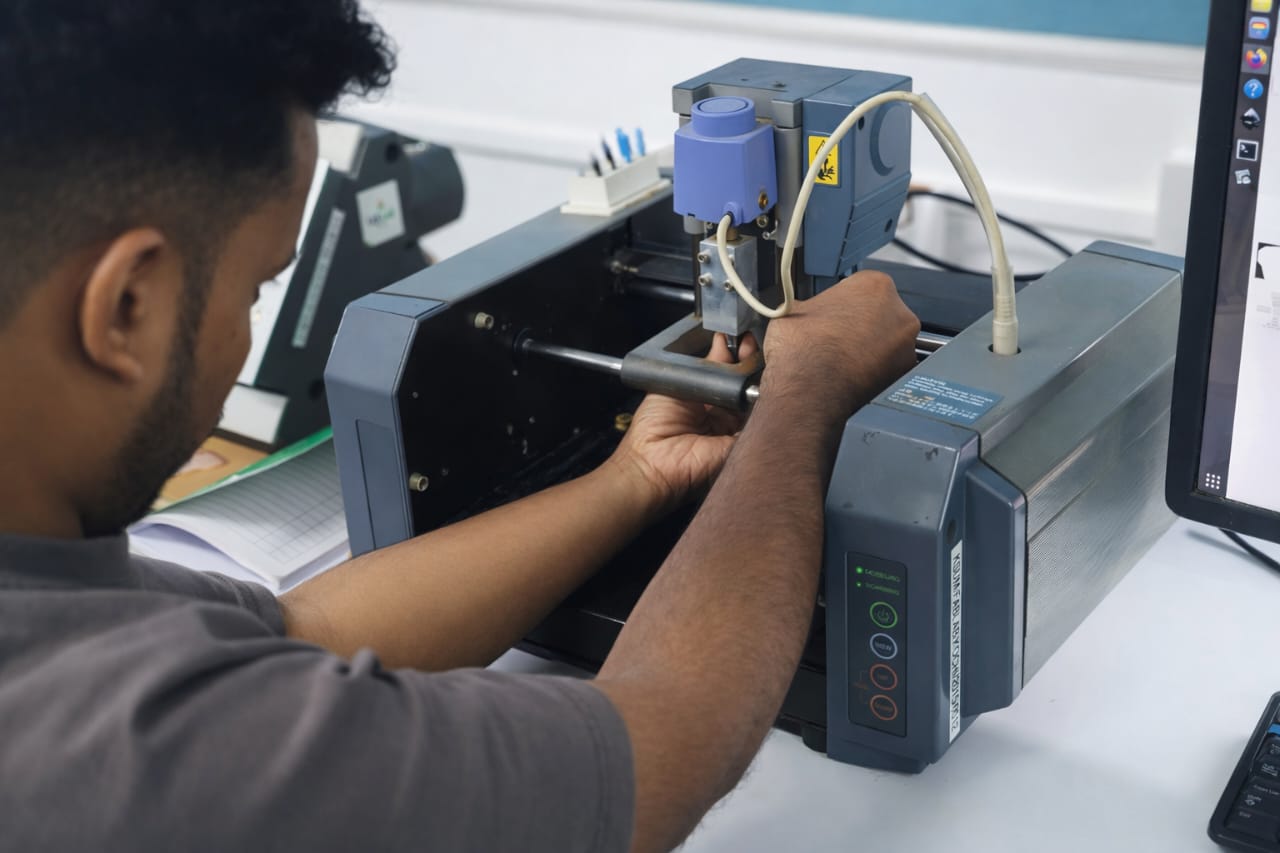
Go to the mods software and then click on position to change bit. This has been set in our lab for the ease of changing the the bit . It is almost at the center of the machine so that our hands could easily maneuver the tool.
Now insert the tool into to the spindle and tighten just enough that the bit won't fall off.
Setting up the Software(Using MODS) and operating the machine.
To make traces.
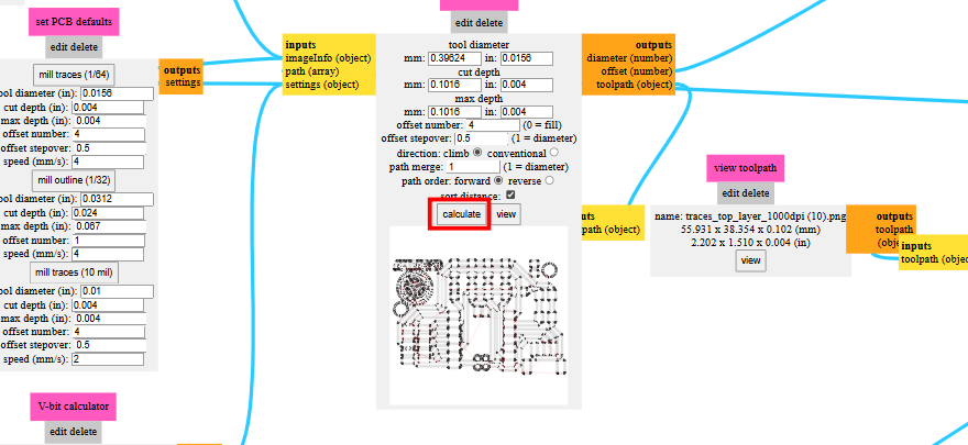
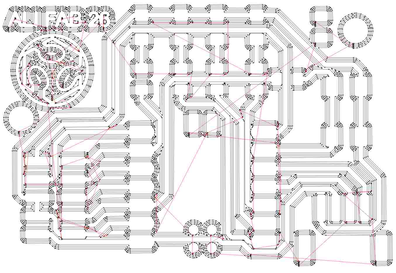
routing and isolation paths
Set the zero position (X, Y, and Z-axis) manually. Adjust milling parameters like spindle speed, feed rate, and depth of cut based on the material and tool specifications. Start the first engraving pass to remove the copper layer and create the circuit traces according to the design. If required, perform multiple passes to ensure clean and accurate cuts, especially for fine or narrow traces.
Once the traces are done ,i moved on to drill holes as it was required in my design. Clean up the dust gatherd after using the machine with a vaccum.
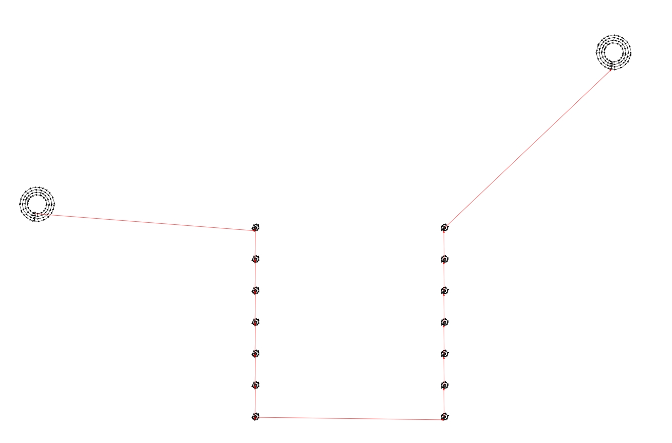
To make Holes and outlines
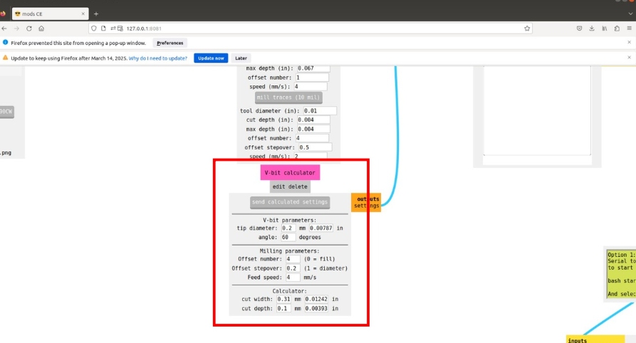
After confirming the values click on calculate. Then we can clcik send file to mmake the machine start the operation.
After the holes are drilled, we can proceed to cut out the Outline of the PCB. We just need to replace the drillhole png with Outline Png for this step as we will be using the same toolbit for this operation.Click on send file to start the process of milling the PCB.
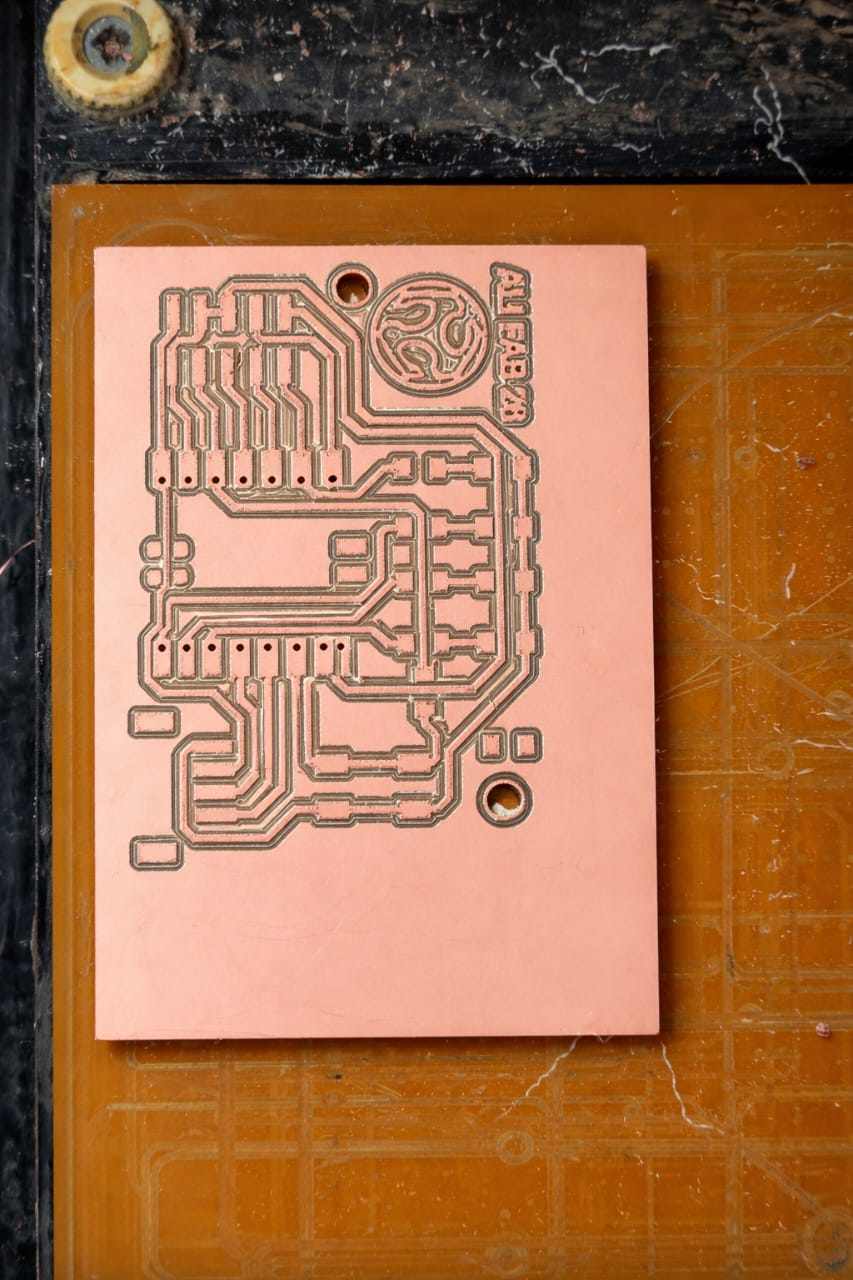
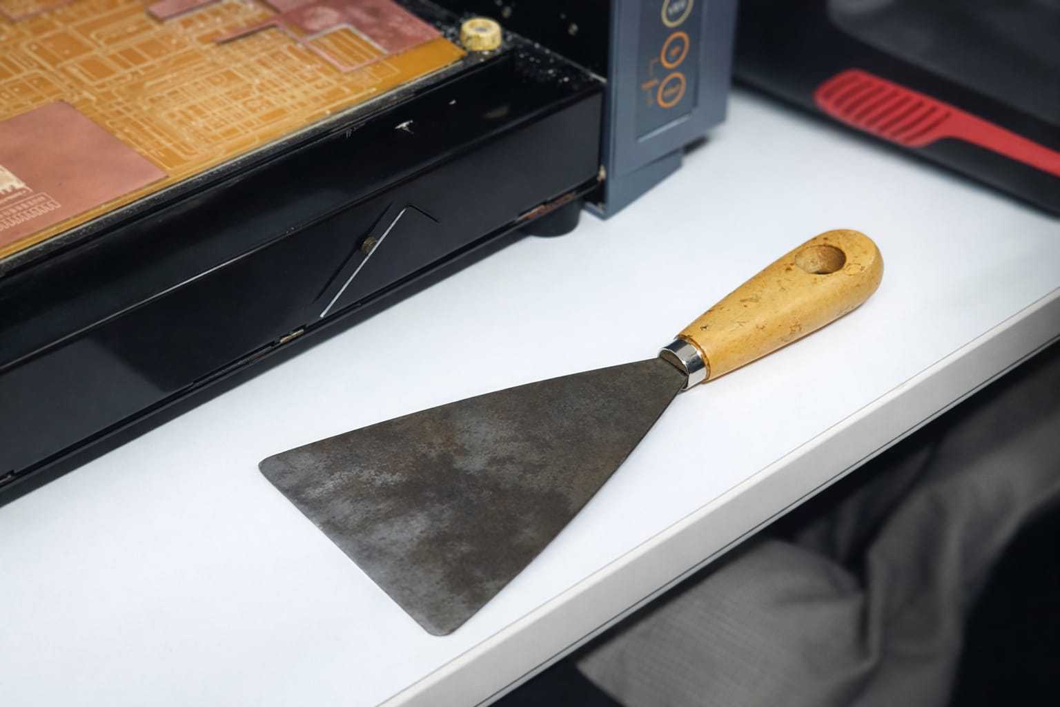
When the milling is completed we can click on view to bring out the bed. Use a scraper to carefully peel out the pCB from the bed. Make sure to clean up the dust gatherd around the machine after using it.
After milling all layers, confirm the cutting is correct, then use a vacuum cleaner to remove dust.
I used a scraper tool to remove the PCB from the sacrificial layer.
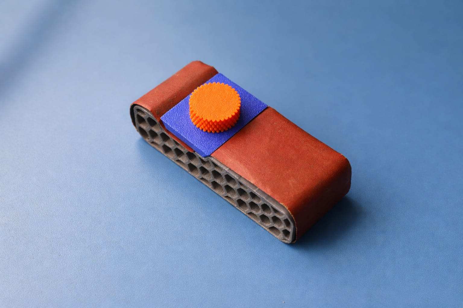
sanding block is used to smooth the PCB surface
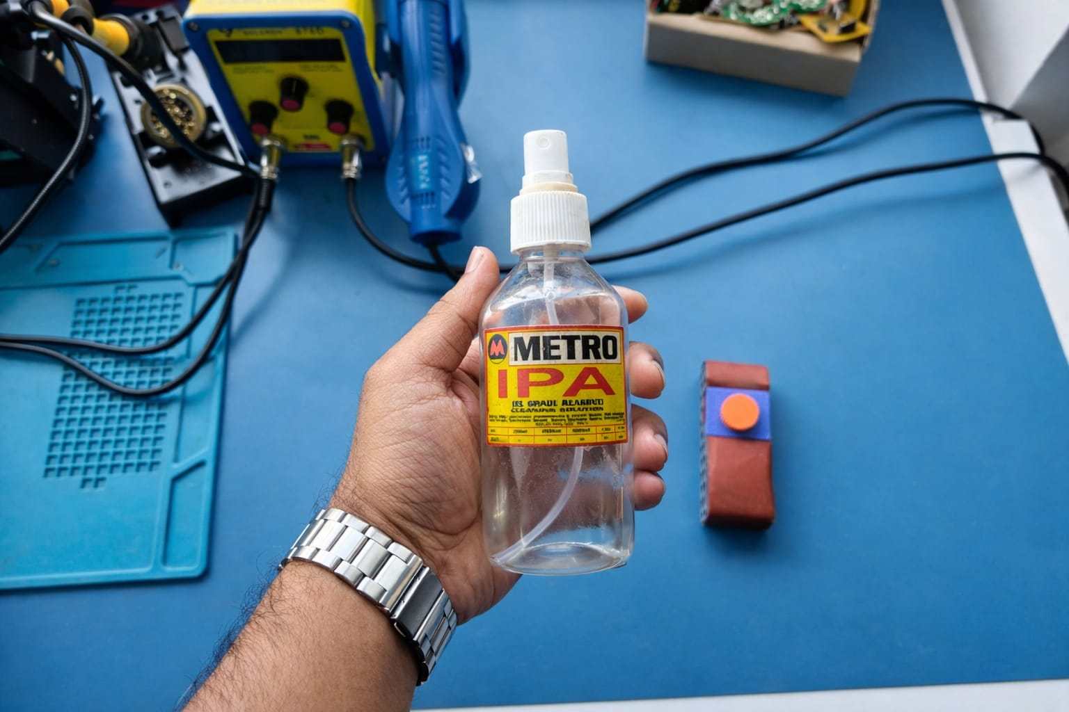
I used IPA (isopropyl alcohol) to avoid scratches and clean the surface.
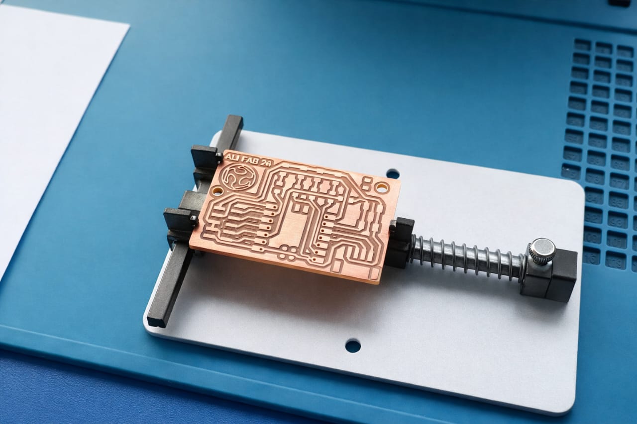
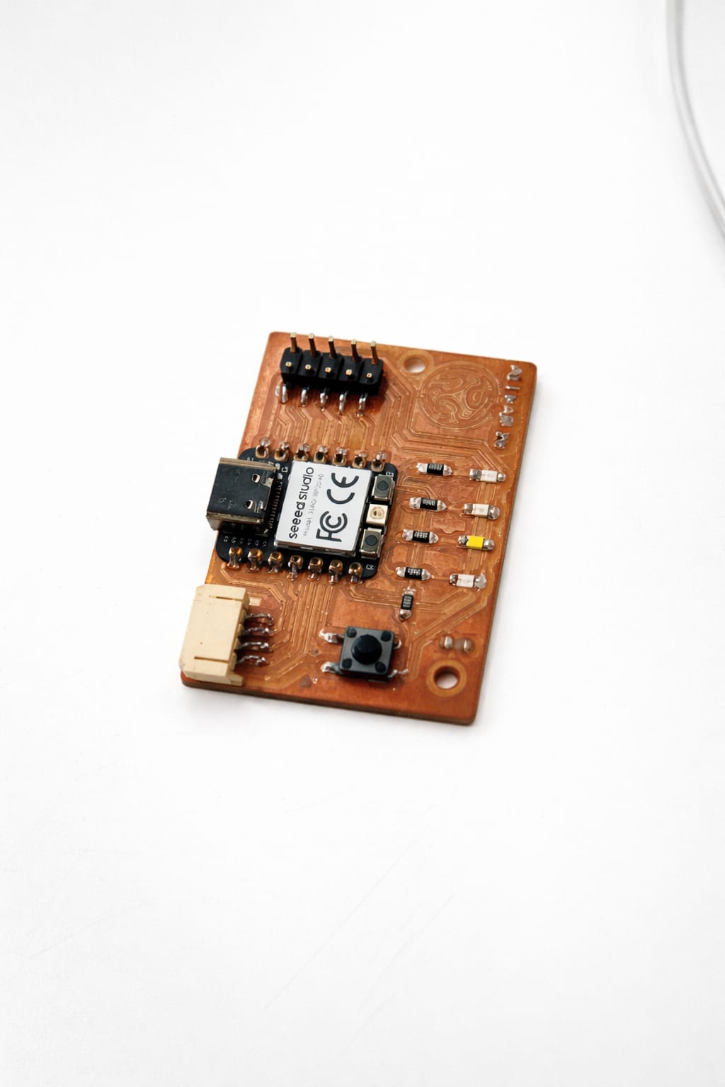
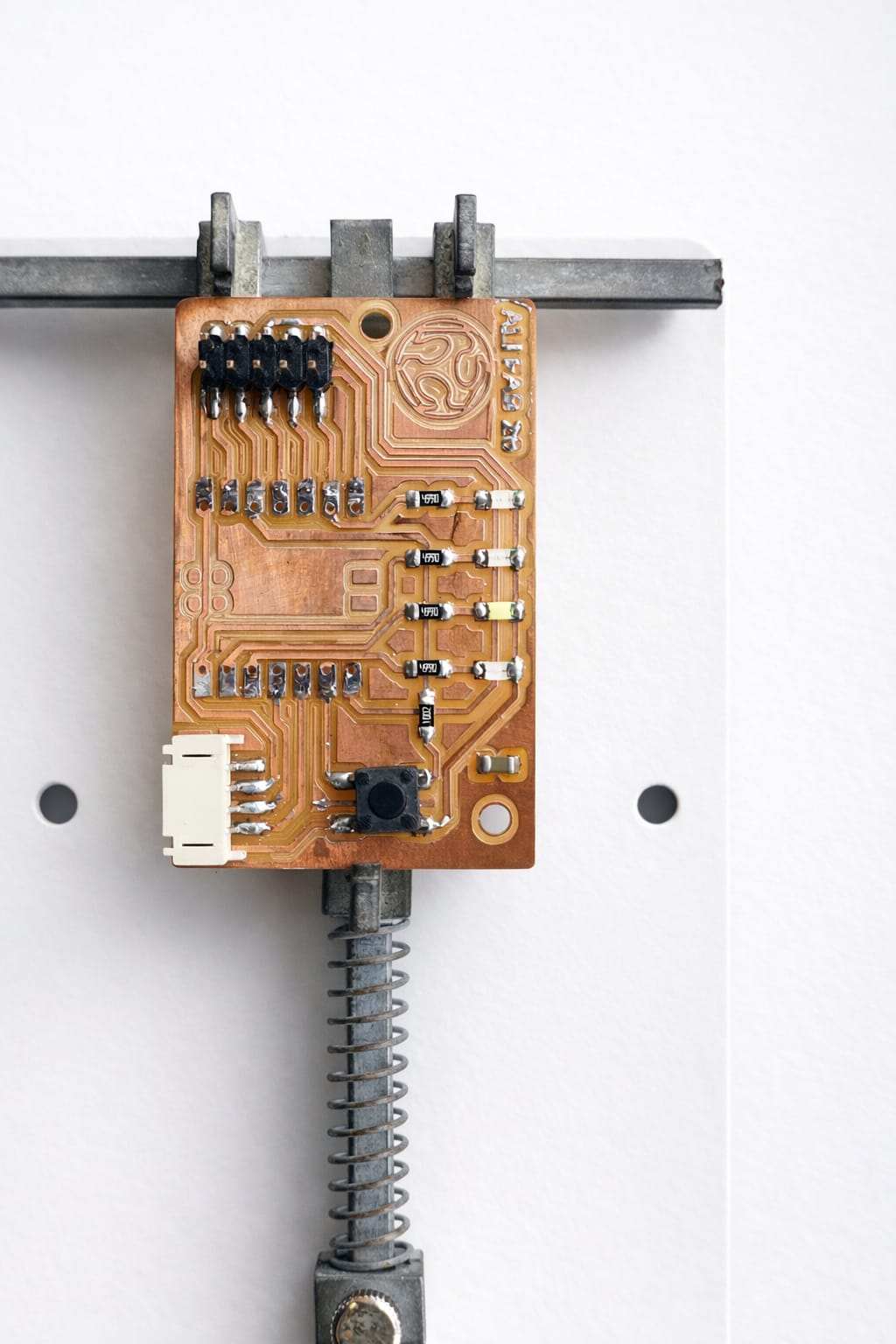
This is the final PCB after post-processing.
The board with the components to be soldered
Soldering and Assembly of the components.
For soldering practice, I used an old PCB and salvaged components. This was my first time working with SMD.
Note: Place all small components solder first.
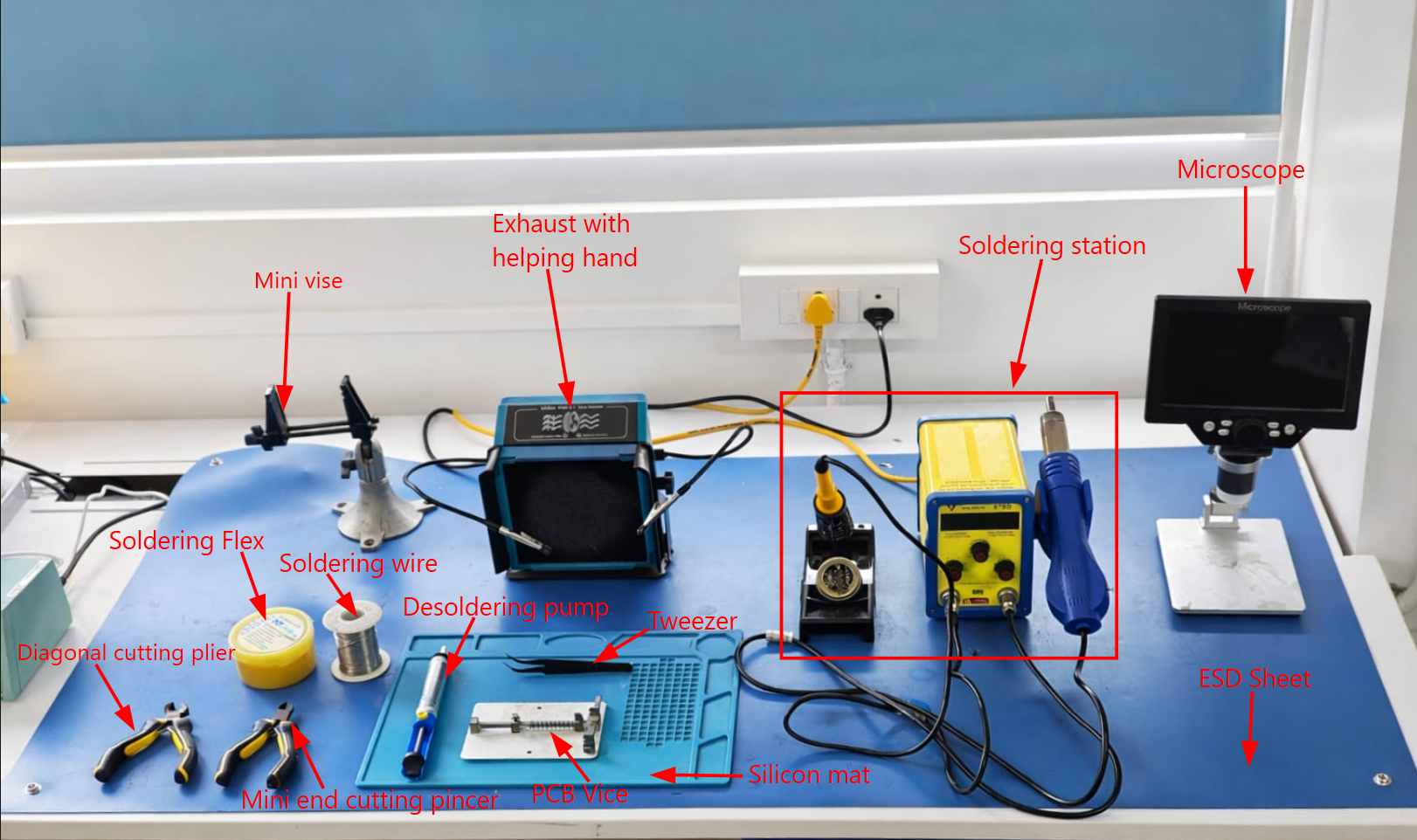
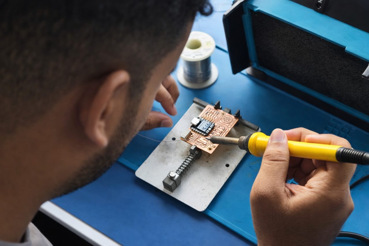
The soldering station was setup as guided and the PCB was clamped to keep it stable.
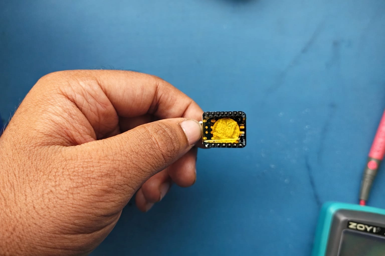
This is my PCB. I need to solder all the components.
Soldering all components one by one.
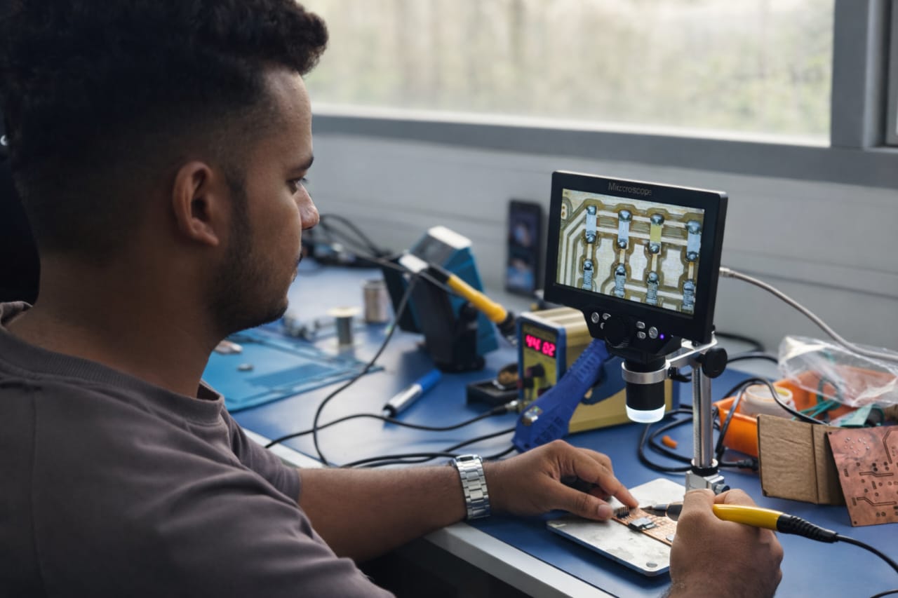
Using a digital microscope, check that all components are properly fixed.
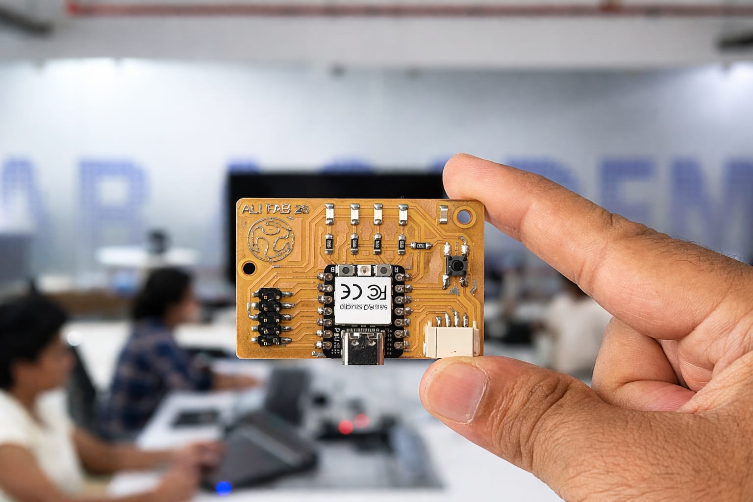
Hero Shot
Code For Making my PCB blink
// LED pins
int ledPins[] = {D0, D1, D2, D8};
int numLeds = 4;

// Switch pin
int switchPin = D5;

void setup() {

  Serial.begin(115200);   // Start serial monitor
  delay(2000);            // wait for serial monitor

  Serial.println("XIAO RP2040 LED Chaser System Started");

  // LED pins as output
  for (int i = 0; i < numLeds; i++) {
    pinMode(ledPins[i], OUTPUT);
  }

  // Switch input with internal pullup
  pinMode(switchPin, INPUT_PULLUP);
}

void loop() {

  int switchState = digitalRead(switchPin);

  if (switchState == LOW) {

    Serial.println("Switch Pressed - LED Chaser Running");

    // LED chaser
    for (int i = 0; i < numLeds; i++) {
      digitalWrite(ledPins[i], HIGH);
      delay(150);
      digitalWrite(ledPins[i], LOW);
    }

  } else {

    Serial.println("Switch Released - LEDs OFF");

    for (int i = 0; i < numLeds; i++) {
      digitalWrite(ledPins[i], LOW);
    }

    delay(500);
  }
}
Error Fount
Steps To Solve
For desoldering, this was my first time, so I practiced on an old board.
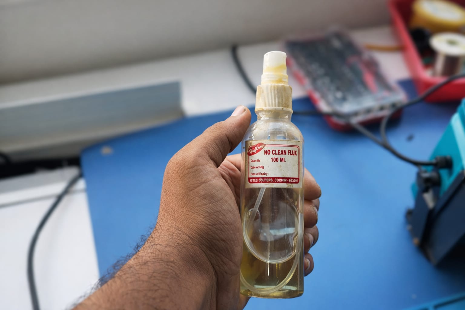
First, I sprayed some flux on both sides of the Xiao.
Then, I used a heat blower at 350°C with medium fan speed, and used tweezers to remove it.
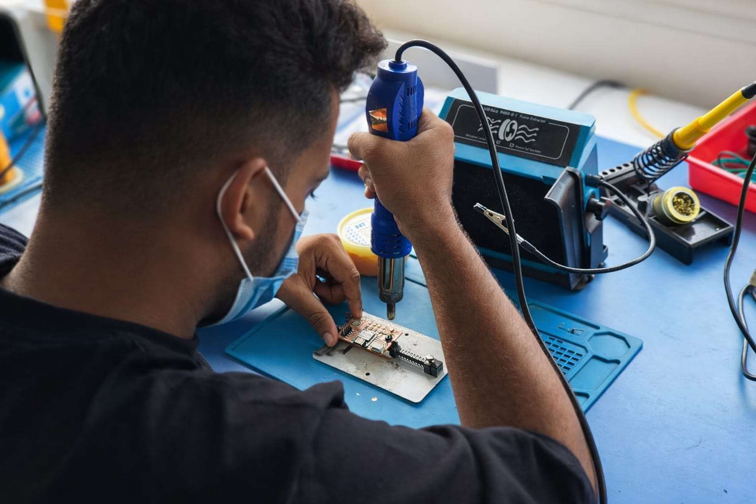
After removing the Xiao, I placed Kapton tape on the bottom side to avoid short circuits.
Then, I cleaned the PCB board to prepare it for resoldering.
Using a knife, I cleared the short circuit path.
After that, I resoldered the Xiao.
I used the USB power meter (JUWEI tester) to test my PCB and confirmed that there were no short circuits and the power was stable.
The USB power meter shows a stable voltage of around 5.09V with a current of 0.052A, indicating normal operation of the PCB.
3D Printed Case Making
Designing and fabricating a 3D printed case is considered extra credit.
I tried to design a case for the PCB in Fusion 360 I exported the file in pcb editor as step file and opened it in fusion.
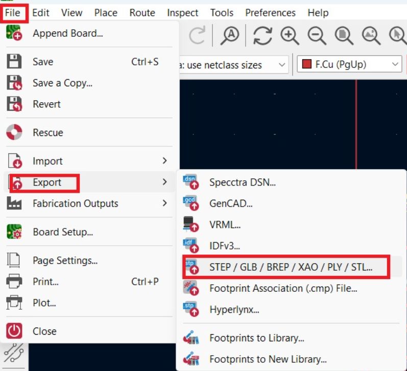
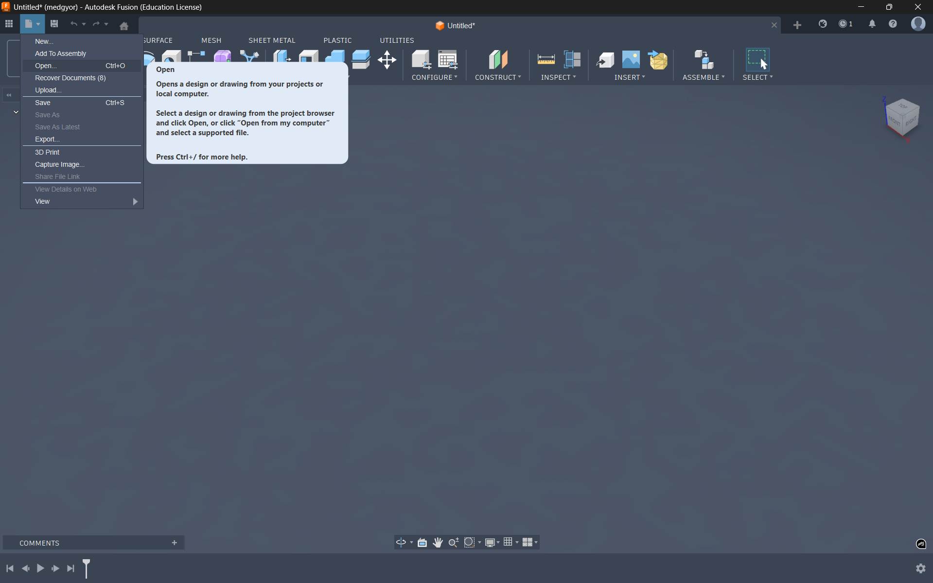
To import file in fusion, open file -> open.
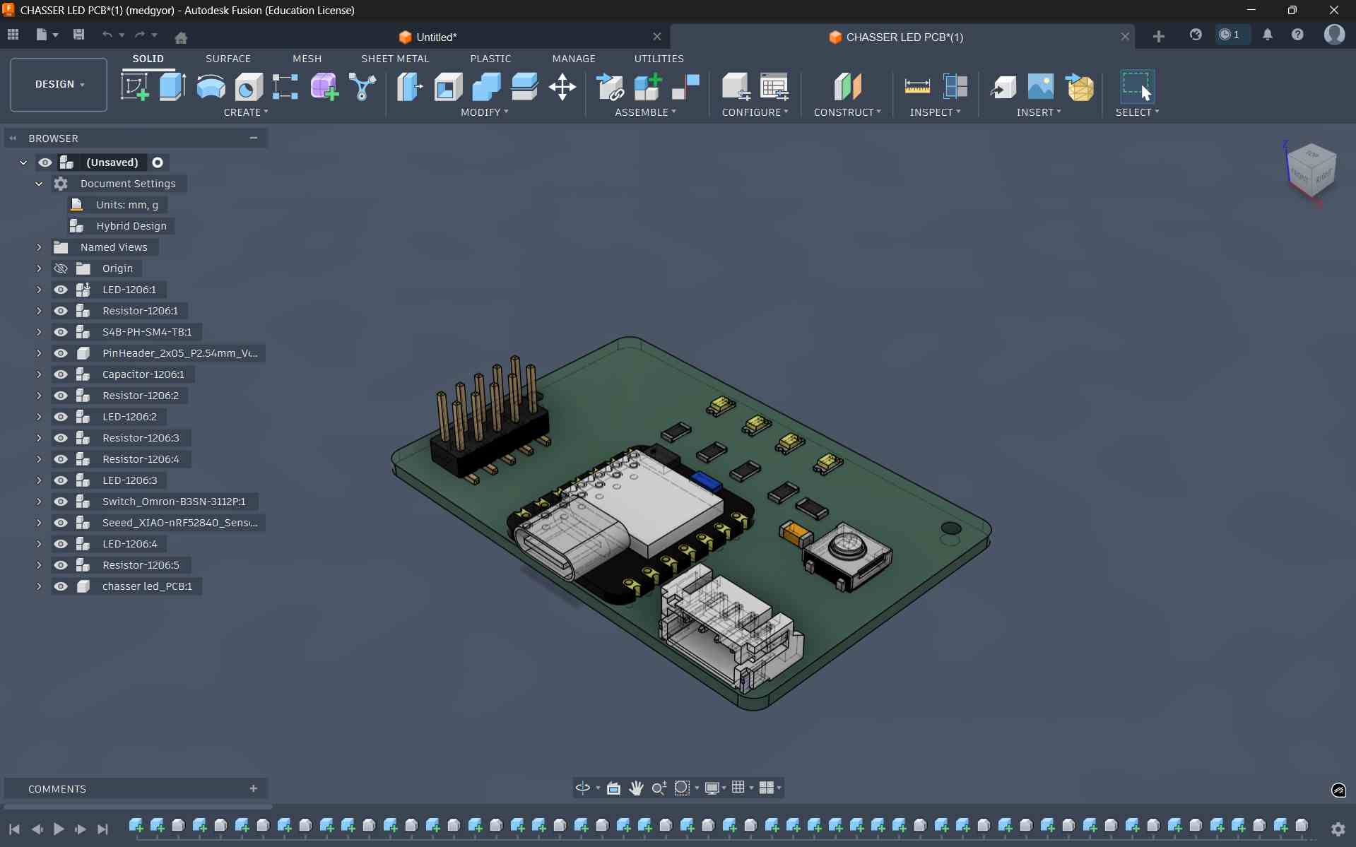
After importing the file, this is how it appears on the screen
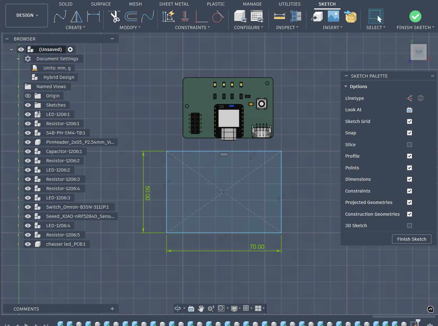
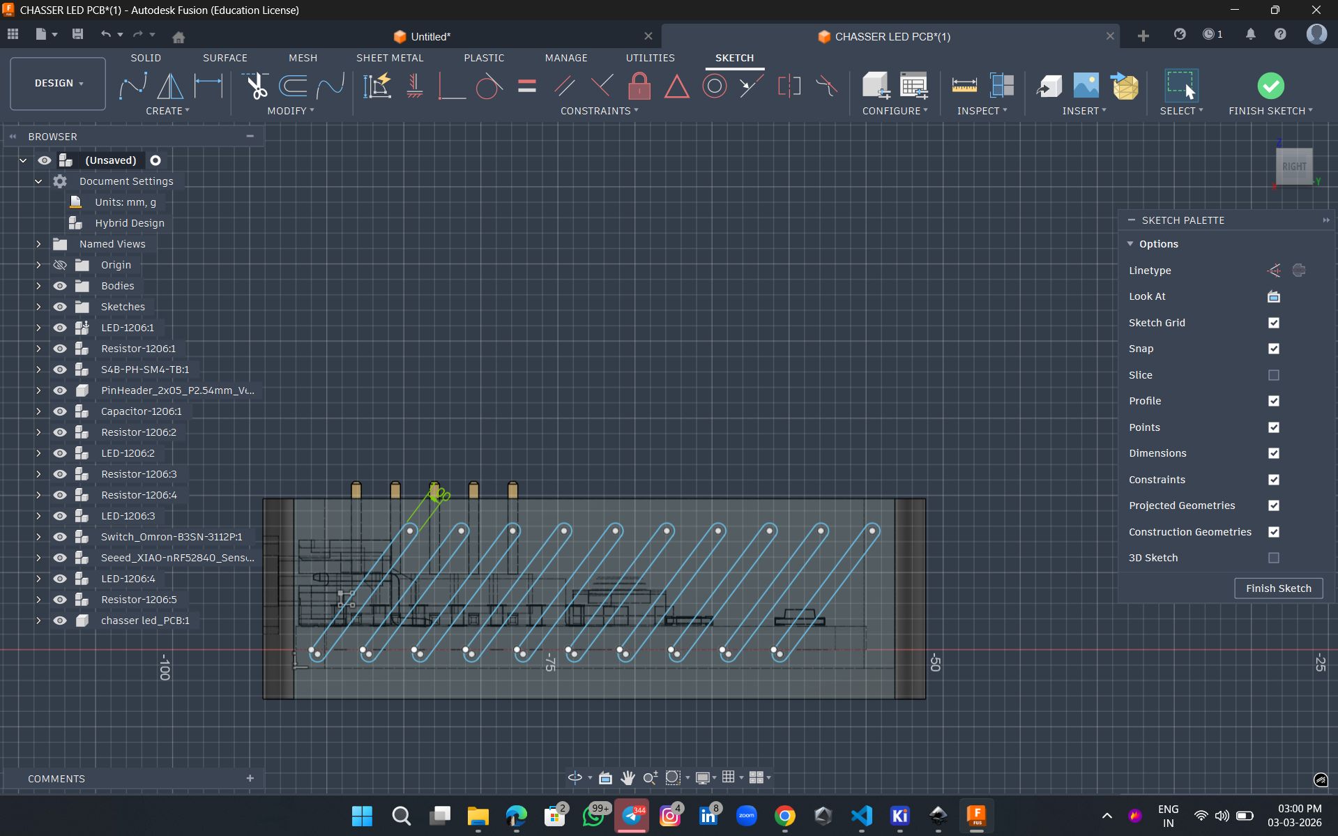
For the enclosure design, I sketched a 50 mm × 70 mm rectangle and extruded it to 15 mm. After that, I applied the shell operation to achieve a uniform wall thickness of 2 mm.
To provide a cable connection, I created a sketch on the top surface of the enclosure and extruded it to form an opening, following the methods learned in Week 02.
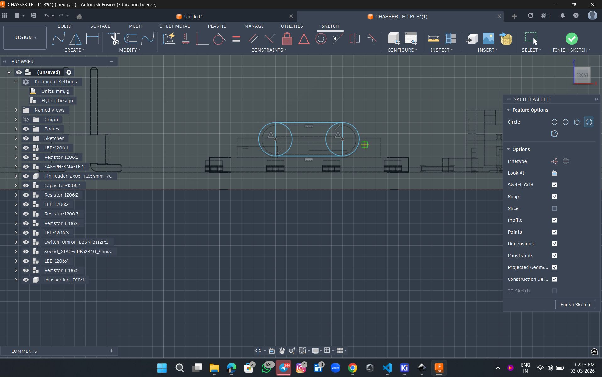
Finally, I added a 2 mm fillet to the corners to improve grip and enhance the overall finish of the enclosure.
To enhance both the grip and aesthetics, I created a surface texture using a patterned design and extruded it to a height of 0.1 mm.
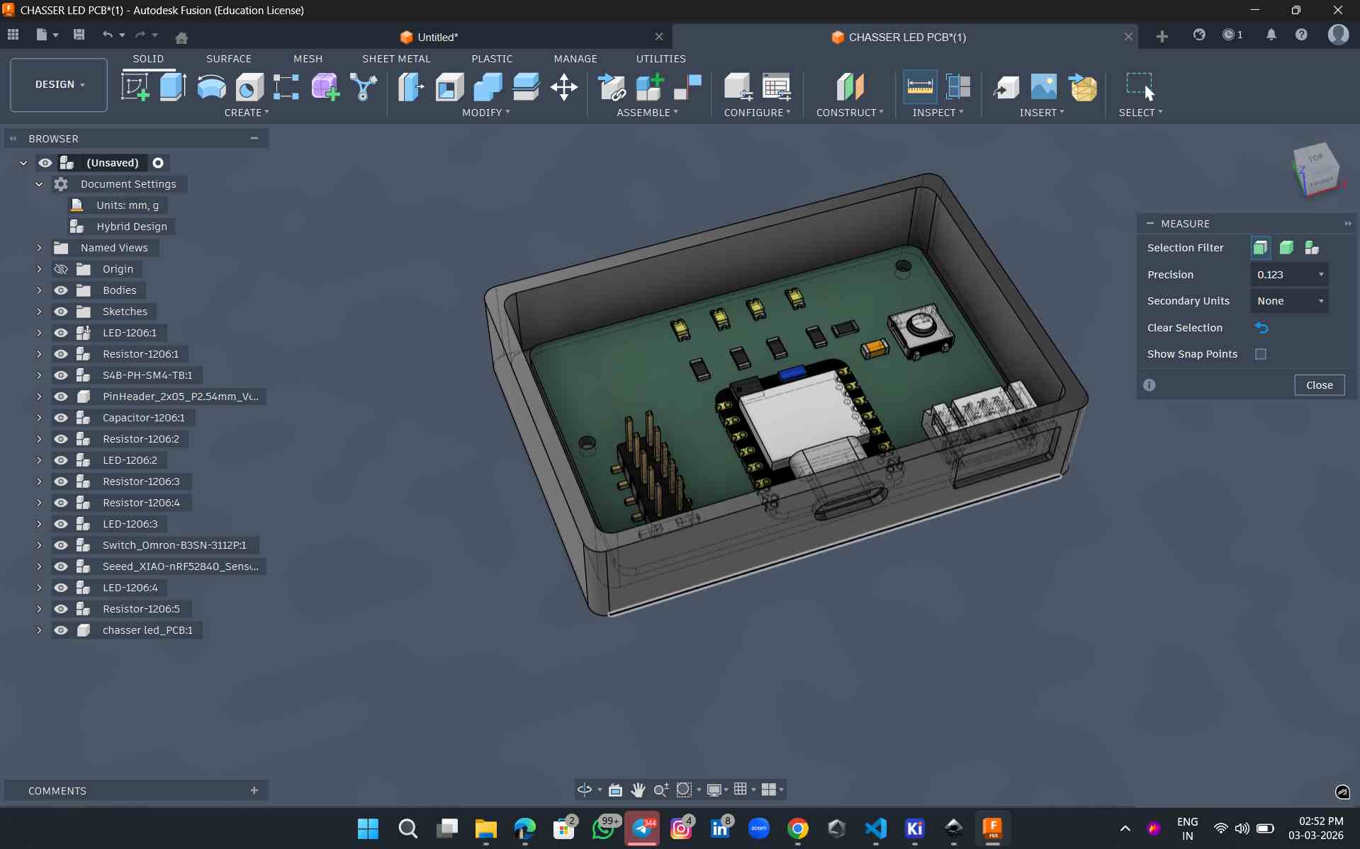
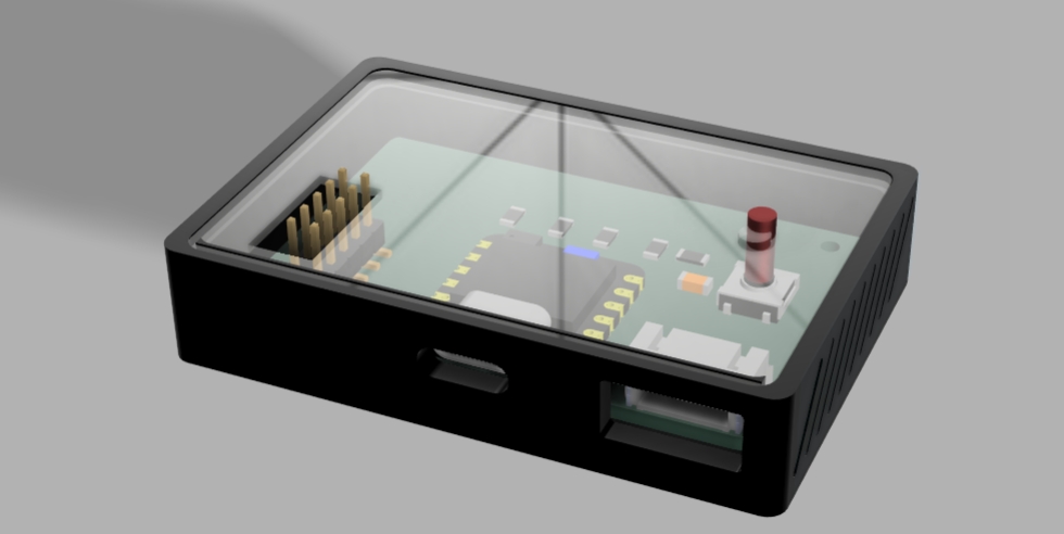
This is the final output after rendering. For the top layer, I am planning to use acrylic, and the remaining body parts will be 3D printed. In the appearance settings, I applied a clear glass material to the top layer to represent acrylic and a standard black finish to the main body
Conclusion
The electronics production process used the Roland Modela MDX-20, including PCB design, milling, soldering, and programming. The circuit was designed in KiCad, and an FR1 PCB was milled using Mods CE. After soldering and testing with a multimeter, the board was programmed in Arduino IDE and verified through LED control functions.