Week 8 – Electronics Production
This week, we will focus on understanding the capabilities of our lab’s PCB milling machine, and based on this understanding I will set the constrains of my PCB. And then, I plan to fabricate a PCB using the milling process, followed by assembling the board by soldering SMD components. Our instructors for this week are Saheen, Sibin, and Revisankar, who will guide us through both the fabrication and assembly processes.
The objective is to understand the design rules of PCB production process, make and test embedded microcontroller system that I designed in Electronic design week.

AI prompt ChatGPT: "Can you please give an animated fun image of myself for this discretion - This week, I will focus on PCB milling machine. And then, I plan to fabricate a PCB using the milling process, followed by assembling the board by soldering SMD components.
Assignment Overview
- Characterize the design rules for your in-house PCB production process.
- submit a PCB design to a board house.
- Make and test an embedded microcontroller system that you designed.
- extra credit: make it with another process
| Day | Activity | Status |
|---|---|---|
| 📘🛠 Thursday | Class - Electronics Production & Group Assignment | Completed |
| 🛠 Friday | Updated my PCB Design and setup for PCB Milling | Completed |
| 🛠 Monday | PCB Milling and Soldering | Completed |
| 📘 Thursday | Individual Assignment Documentation, Group Assignment Documentation | In progress |
| 📘🛠 Wednesday | PCB Testing and Documentation | Completed |
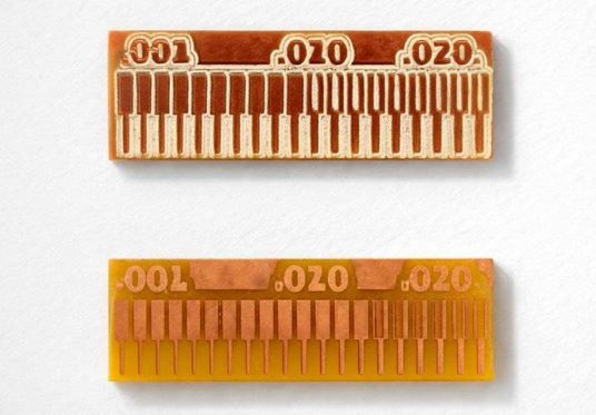
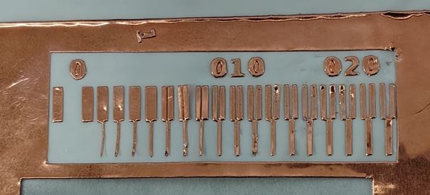
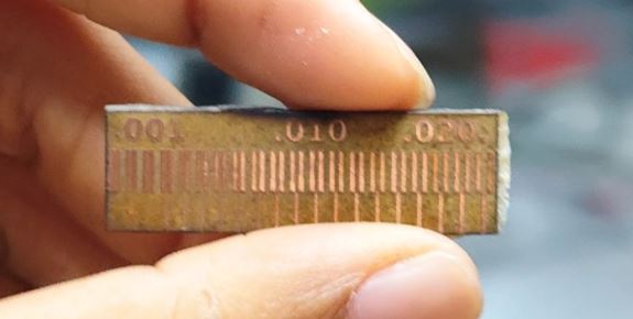
Group Assignment
In this week’s group assignment, we evaluated the minimum trace width and the minimum spacing between tracks that can be reliably achieved using our PCB milling machine Roland Modela MDX 20, Vinyl Cutter Roland CAMM-1 and Leaser cutter X Tool.
PCB Design - Verifying Constrains
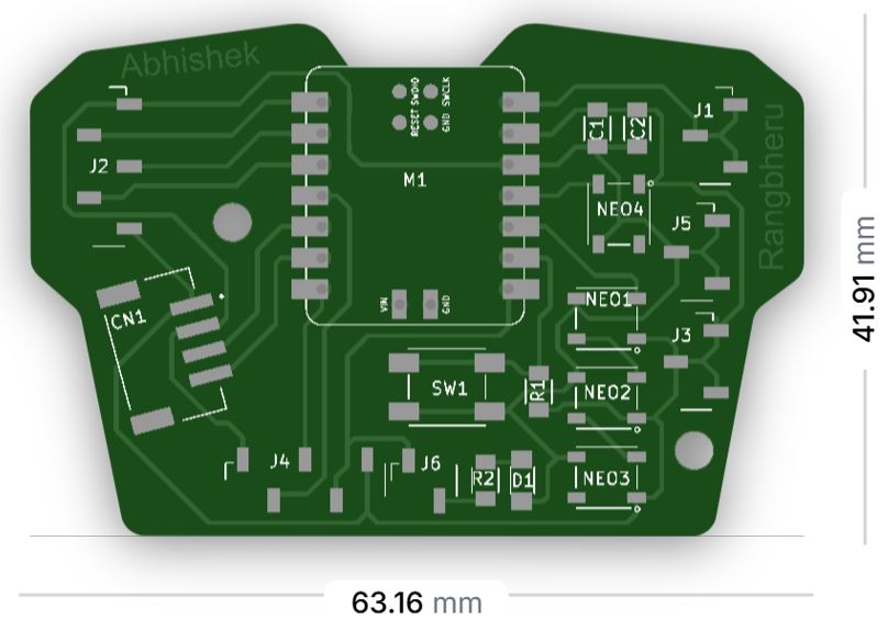
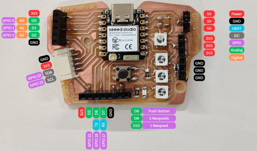
Below is the design from my Electronics Design Week that I’ll be producing this week. I made a few small tweaks to improve the layout and usability. I added a right-angle sliding switch (highlighted in the green box) to easily turn the battery ON and OFF. Since the PCB size was originally 50 mm × 70 mm, I adjusted the component placement, bringing them slightly closer in the Y-direction. For the next iteration, I plan to include a push-button with a latching circuit for power control.
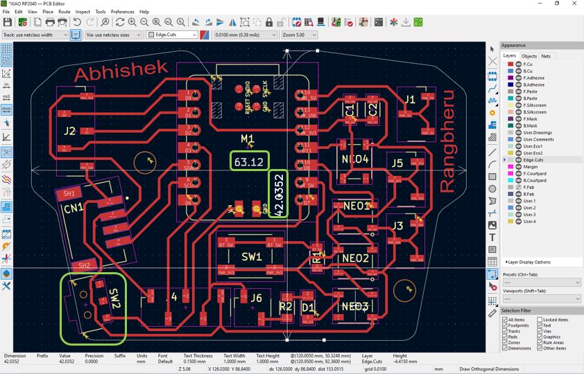
Based on our Group Assignment, we verified the design rule constrains that we gave during Electronics Design Week.
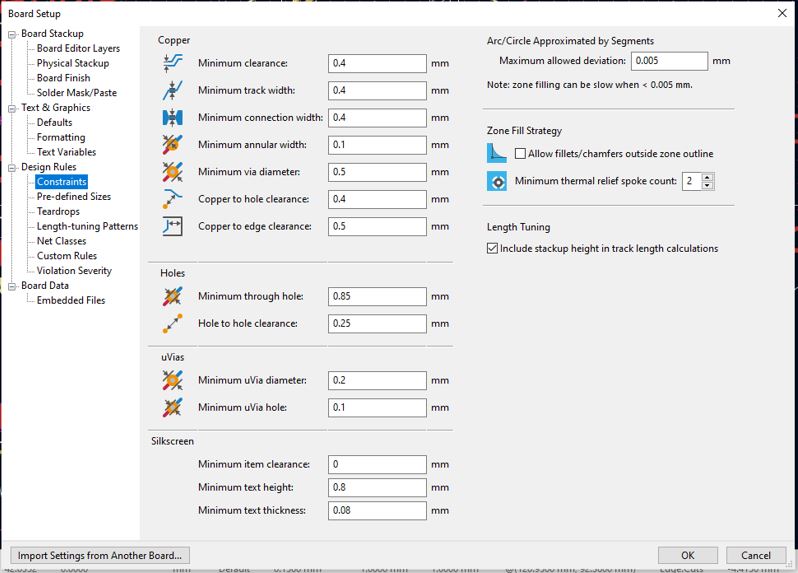
I asked AI to explain above constrains and made a table for my future reference. Prompt : can you please help me to understand each of these constrains in the attached image?
| Constraint Name | What it Means | Why it is Important | Extra Information |
|---|---|---|---|
| Minimum Clearance | Minimum gap between any two copper elements | Prevents short circuits between tracks, pads, and vias | Think of it as a "no touching zone" between electrical paths |
| Minimum Track Width | Smallest width allowed for PCB traces | Too thin traces can burn or break; affects current capacity | For milling, this is limited by the tool diameter (e.g., 0.4 mm safe) |
| Minimum Connection Width | Width of copper connections in zones or pads | Ensures strong and reliable electrical connections | Usually kept same as track width for consistency |
| Minimum Annular Width | Copper ring around a drilled hole (via/pad) | Prevents pads from breaking or lifting off | Acts like a safety ring around the hole |
| Minimum Via Diameter | Total size of the via including copper | Too small vias cannot be drilled properly | For PCB milling, vias are often avoided or kept large |
| Copper to Hole Clearance | Distance between copper and non-plated holes | Prevents unintended electrical contact | Important when using mounting holes |
| Copper to Edge Clearance | Distance between copper and PCB edge | Avoids copper exposure and mechanical damage | Helps prevent shorting with enclosure or casing |
| Minimum uVia Diameter | Total size of microvias used in multilayer PCBs | Ensures manufacturability in advanced PCB fabrication | Not used in PCB milling; mainly for high-density industrial boards |
| Minimum uVia Hole | Drill size of microvias | Defines smallest possible via hole in advanced designs | Can be ignored for Fab Lab or basic PCB workflows |
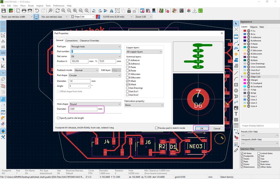
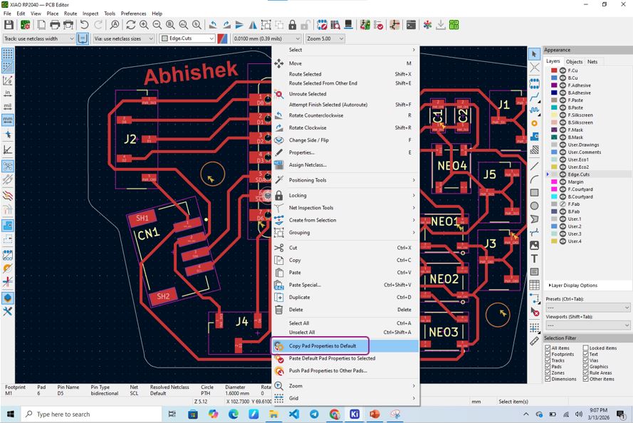
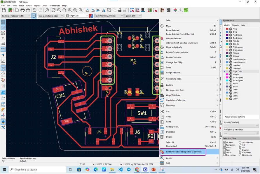
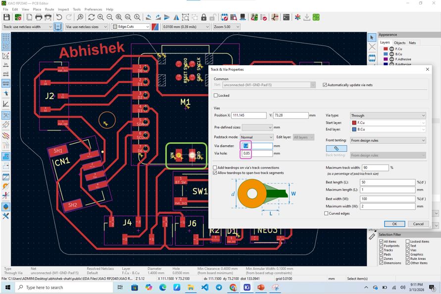
As our drill bit size is 0.8 mm, we need to update the DRC constrains. And increase the hole size of XIAO pad holes to 0.85 mm. first, I update one pad property and then copy that updated pad property then selected remaining XIAO holes and used paste default pad property to selected. Click any of the XIAO hole pad >> Right click >> Properties >> Diameter : 0.85 mm >> click Ok >> again right click same hole pad >> copy pad property to default >> select all the remaining hole pads >> paste default pad property. By doing this all the XIAO pads will be updated with the 0.85 mm dia drills.
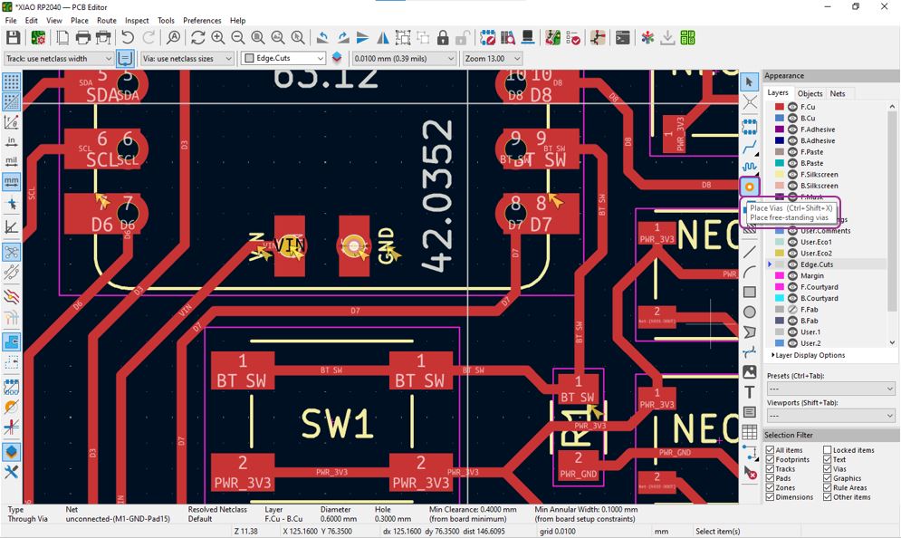
Track and Via hole, as I wanted to use battery my instructor Saheen guided me for adding the via hole becasue the VIN and GND for battery connection are on the back side of XIAO thus after soldering, I will not able to excess it. Thus, we need to a via hole. Select Place Vias >> Place the Vias on the VIN and GND pads >> double click the placed Vias >> update via diameter : 1.4 mm and Via hole : 0.85 mm >> Click Ok.
.
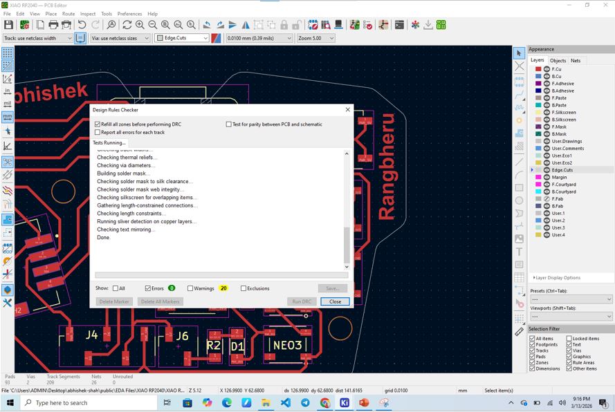
After updating all and before preceding for gerber generation it is very important to perform DRC - Design Rule Check and verify the update the 3D viewer.
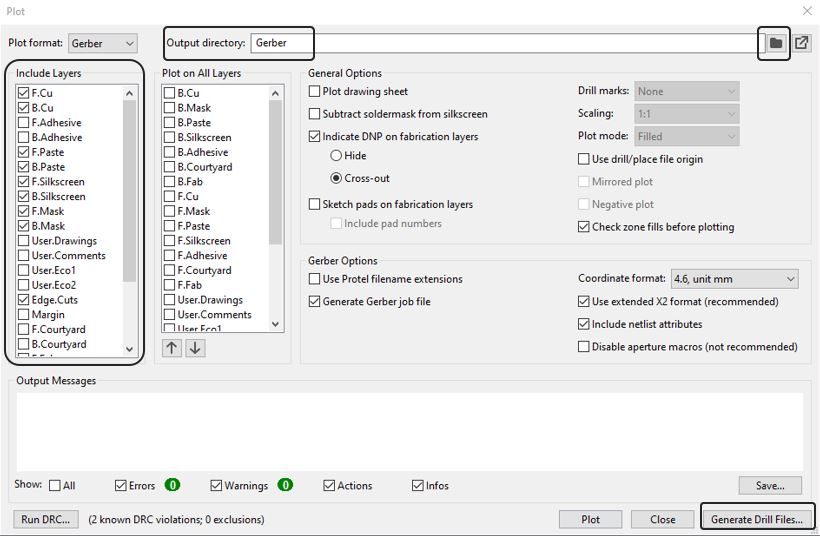
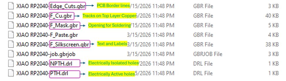
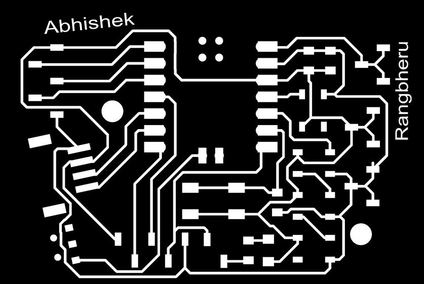
Now, I generated the Gerber files. They are considered as instruction files that machine understands, this is very important when the PCB is sent to the factory for fabrication. The Gerber file contains information about PCB layers for example Copper layers (tracks and pads), Drill information, Edge cut / board outline information etc. The steps to generate gerber files is documented in my week 6 - Electronics Design Week.
For my future reference and understanding, I am adding a video of PCB making process in a factory.
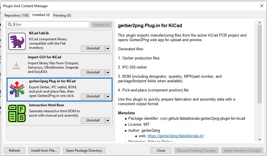
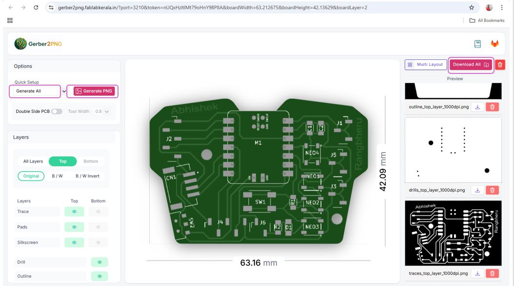
Gerber to PNG generation (FABLAB Kerala Plugins) & Interactive BOM Generation
In our case, PCB MIlling in FABLAB, we usually need PNG/SVG of Top layer, Bottom layer (if applicable), Drills and Border line.
I used Gerber to PNG plugin made by FABLAB Kerala to generate the PNG image of my Traces Top layer, Drill Top Layer and Outline Top layer. More details about Gerber2Png. Later in my documentation these images, I will open in modesCE for PCB milling in the FABLAB
.
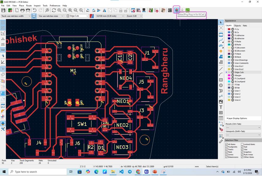
Now, I clicked on Gerber2Png plugin icon >> a new window will open in the browser >> Click Generate PNG >> Download All .


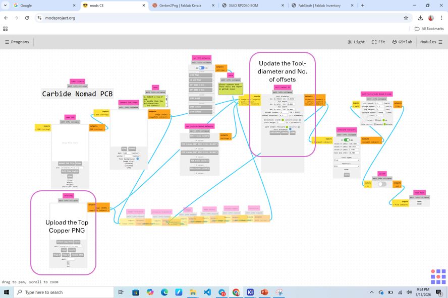
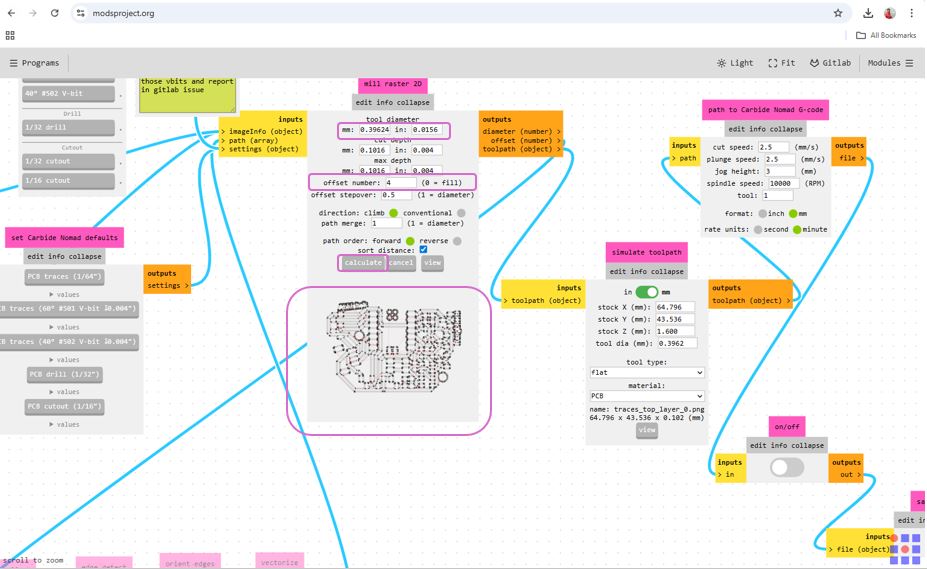
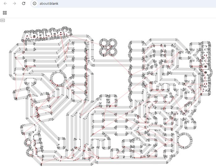
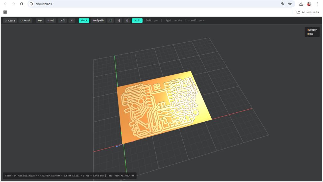
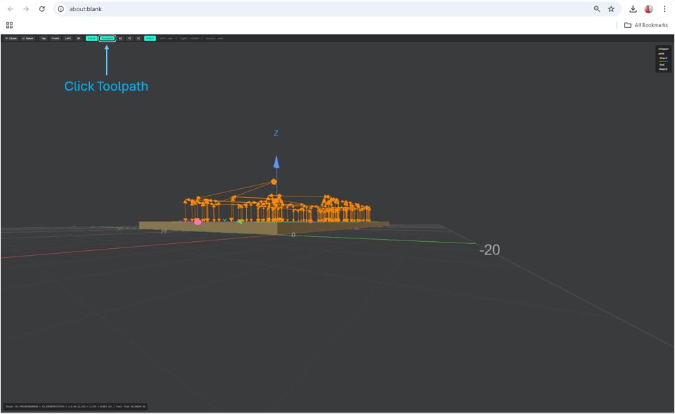
At this stage, using online modesCE, I check the toolpaths in 3D and 3D and get the idea of final PCB outcome. Here I pats are appearing to near then we can go back and rearrange the components and re-draw the paths.
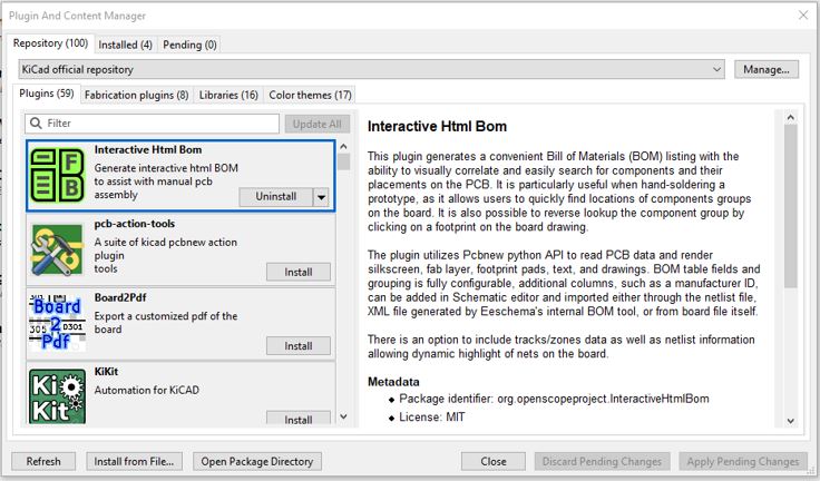
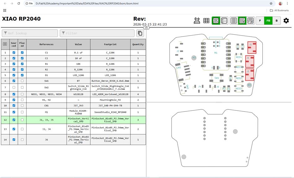
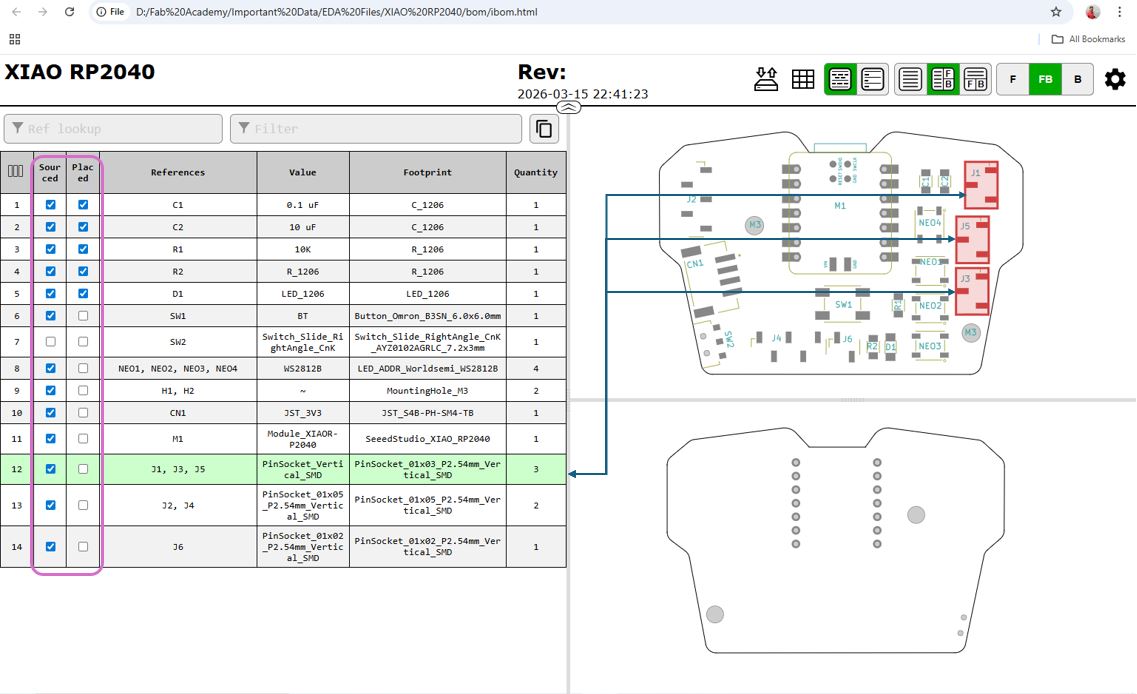
Next, I generated an interactive BOM (Bill of Material) by using from a KiCAD plugin - Interactive HTML BOM. To generate the BOM Click the HTML BOM icon >> set the Directory / BOM Destination >> Generate BOM .
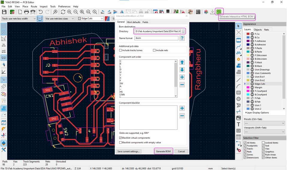
Later after Milling the PCB, this BOM will be very useful in collecting, organizing and soldering the components onto the PCB.
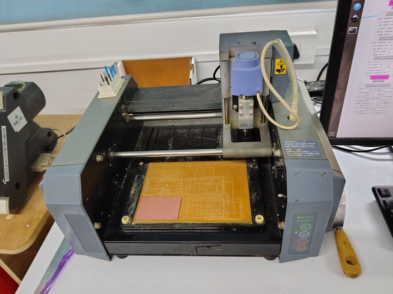
PCB Milling
We have Roland Modela MDX-20 milling machine in our lab. It is a is a 3-axis desktop milling machine.
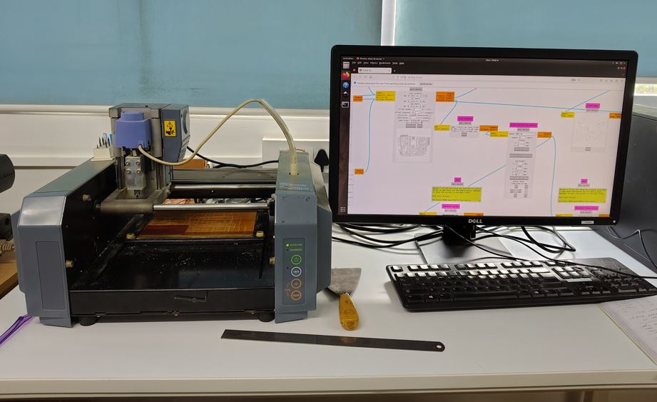
To mill my PCB I need to perform three major operations - Traces Top layer, Drill Top Layer, and Outline Top layer.
Milling the Traces Top layer
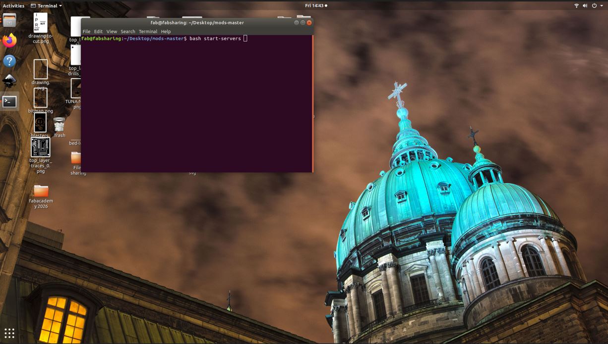
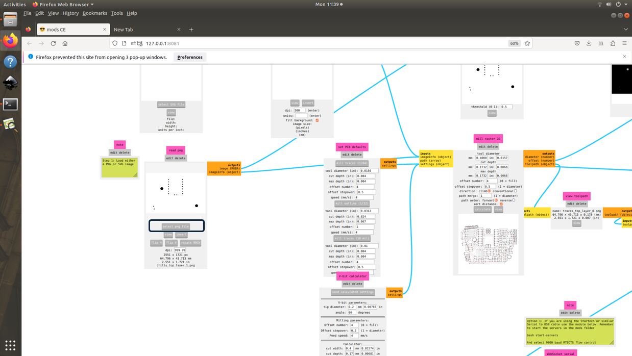
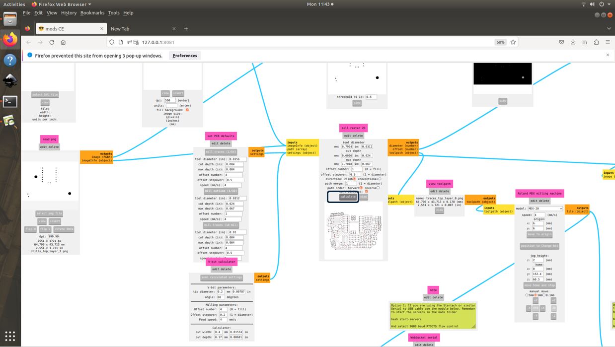
The first thing that I did is I opened the offline modes in the PC and opened the Traces Top layer PNG file of that I got from Gerber to PNG plugin.
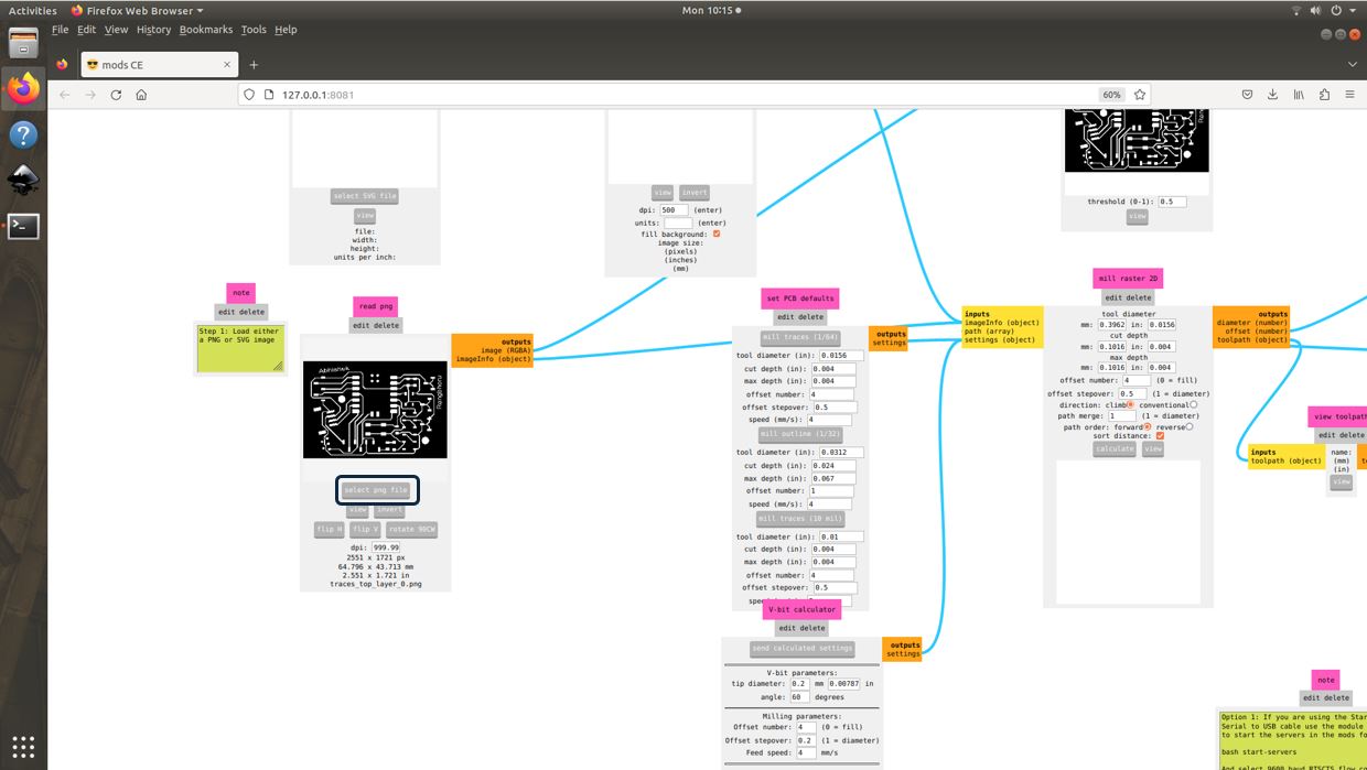
We are going to use V-bit 0.2 mm End mill for milling the Traces. We are using this end mill instead of 1/64 end mill because the 1/64 tip is very fragile and we need practice to use it, thus initially we are using V-bit 0.2 mm End mill.
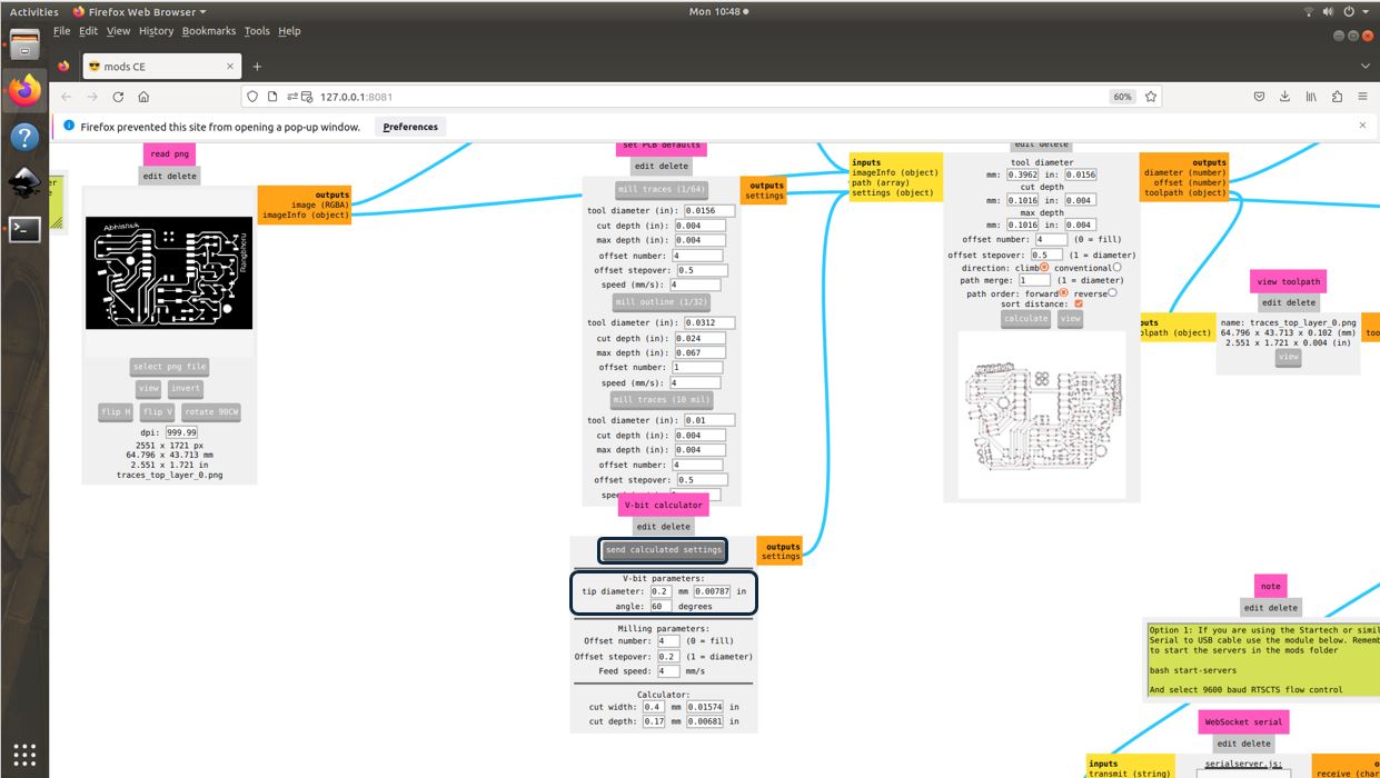
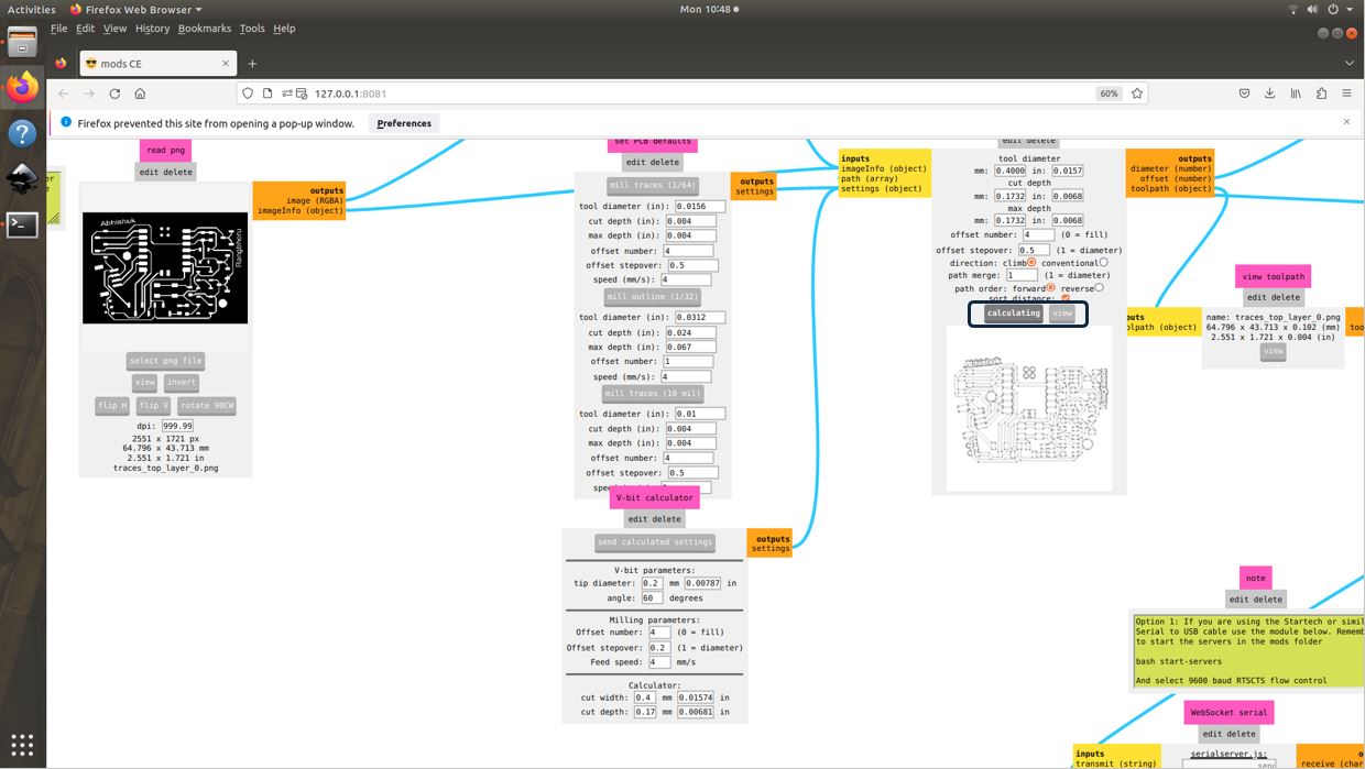
Now I entered Offset numbers, offset stepovers ant then Click Calculate doing this will calcualte the vector toolpath for milling the top layer traces.
Then, I moved the clicked the Position to Change Bit.

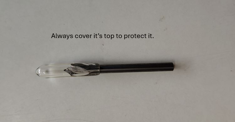
We need to be very careful while changing the tool but always keep your one hand under the tool bit so that it does not fall on the bed and break its tip. And attach the bit key back to the magnet.
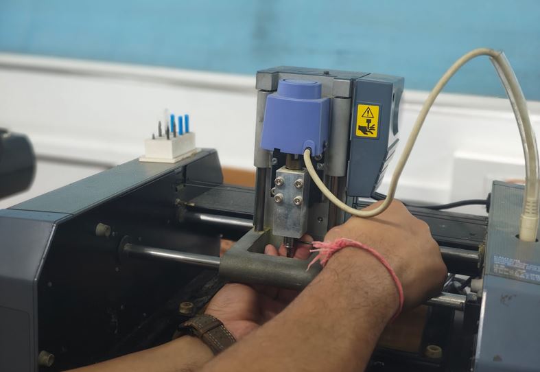
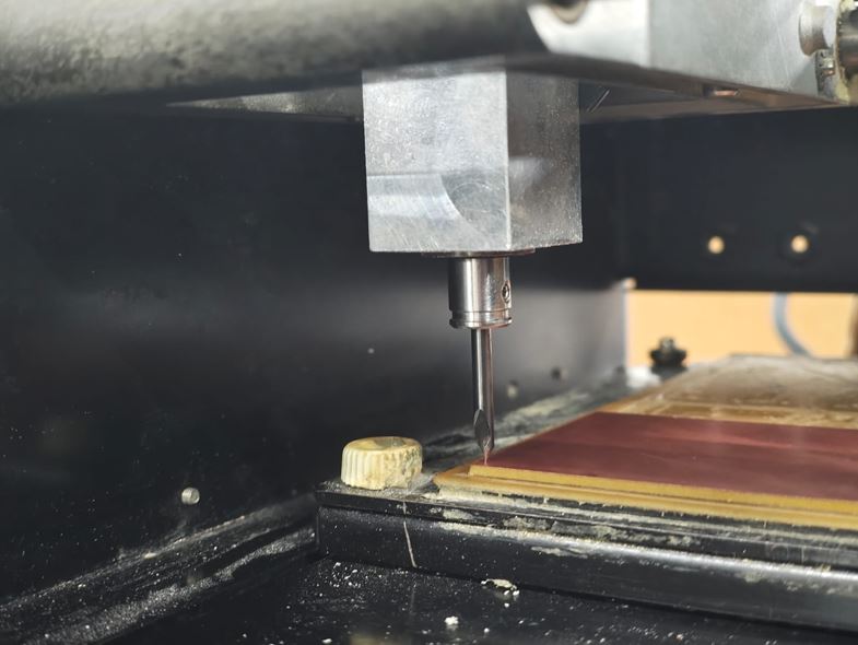
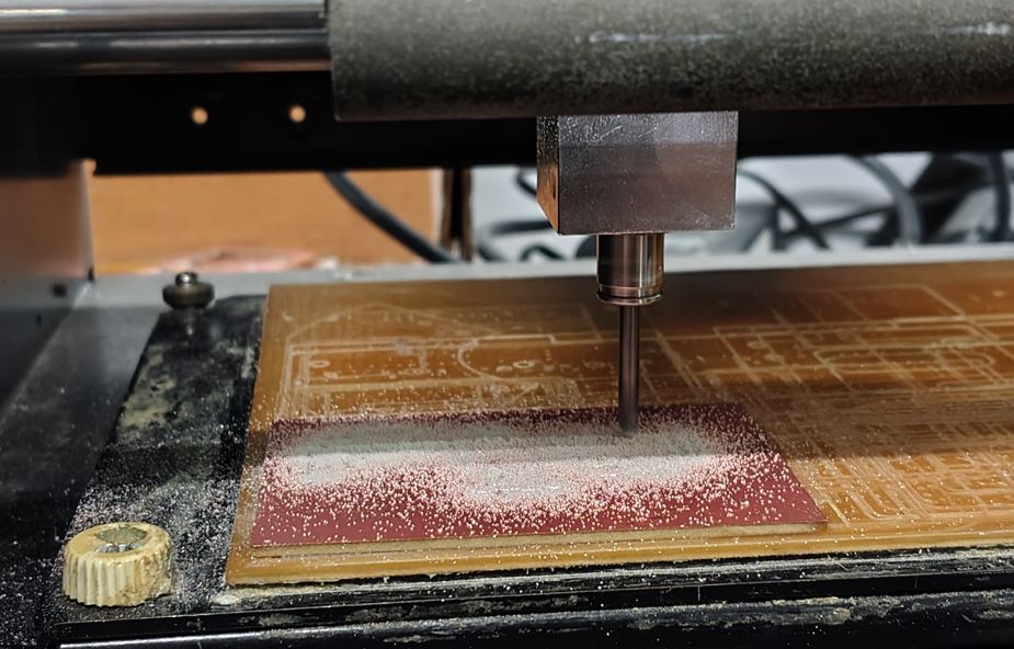
After this, I pressed the view button on the console of the machine so that the bed will come forward and I can stick my copper clad PCB on the bed.
Important always clean the bed using brush and vacuum before sticking the PCB on to the bed.
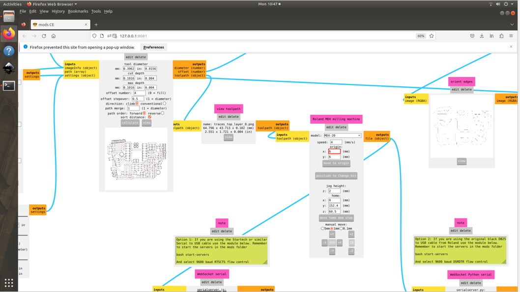
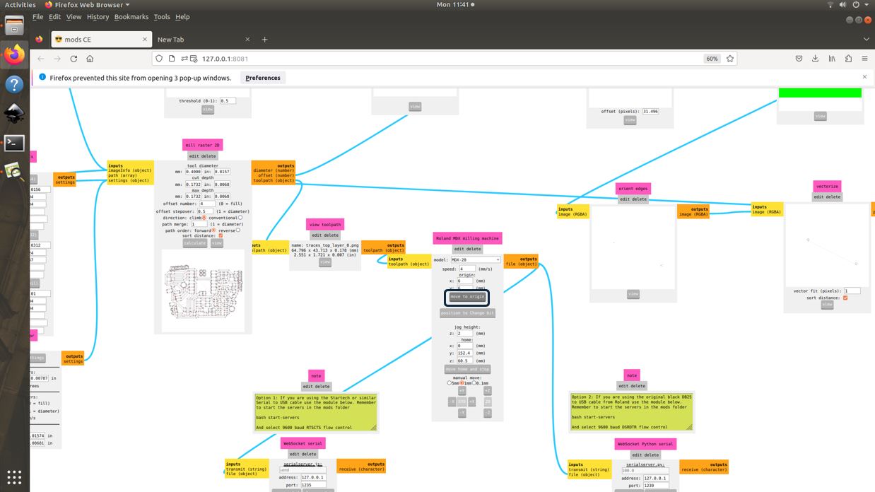
Then, using scale I measure the approximate X and Y distance of the object from the bed origin (0,0). This values I entered in Modes.
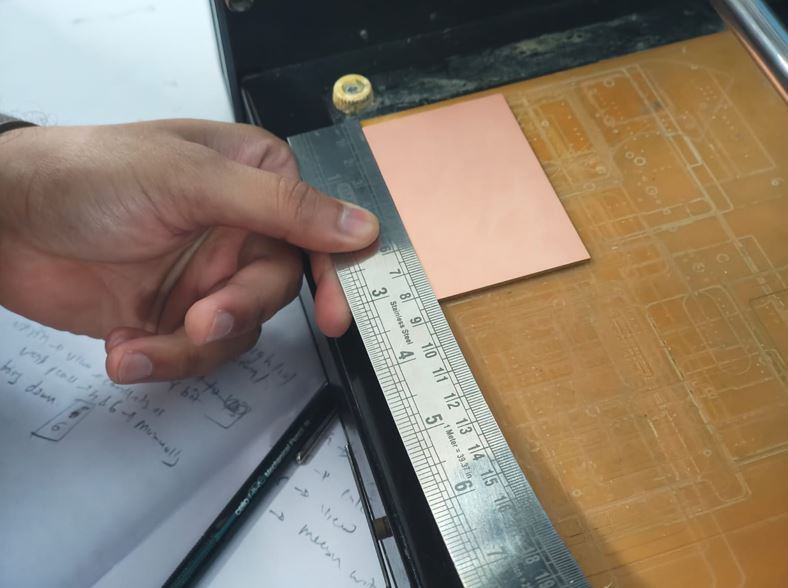
I entered these X = 4 mm and Y = 6 mm values in to modes and press Move to Origin.
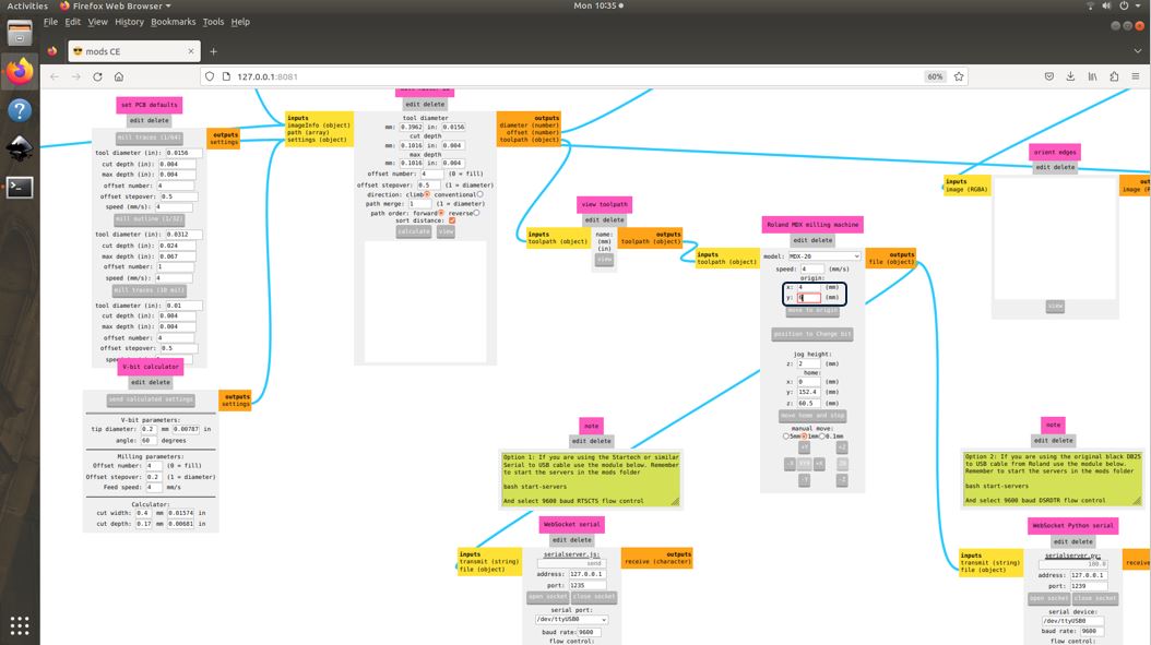
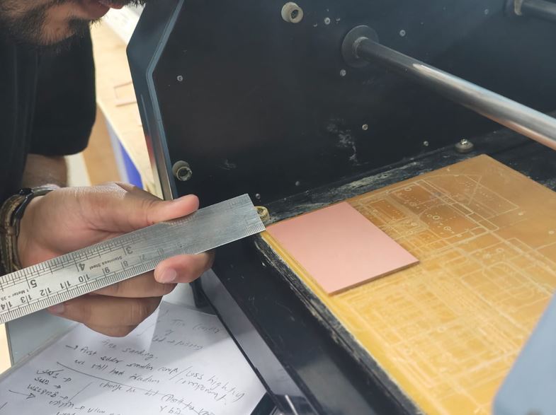
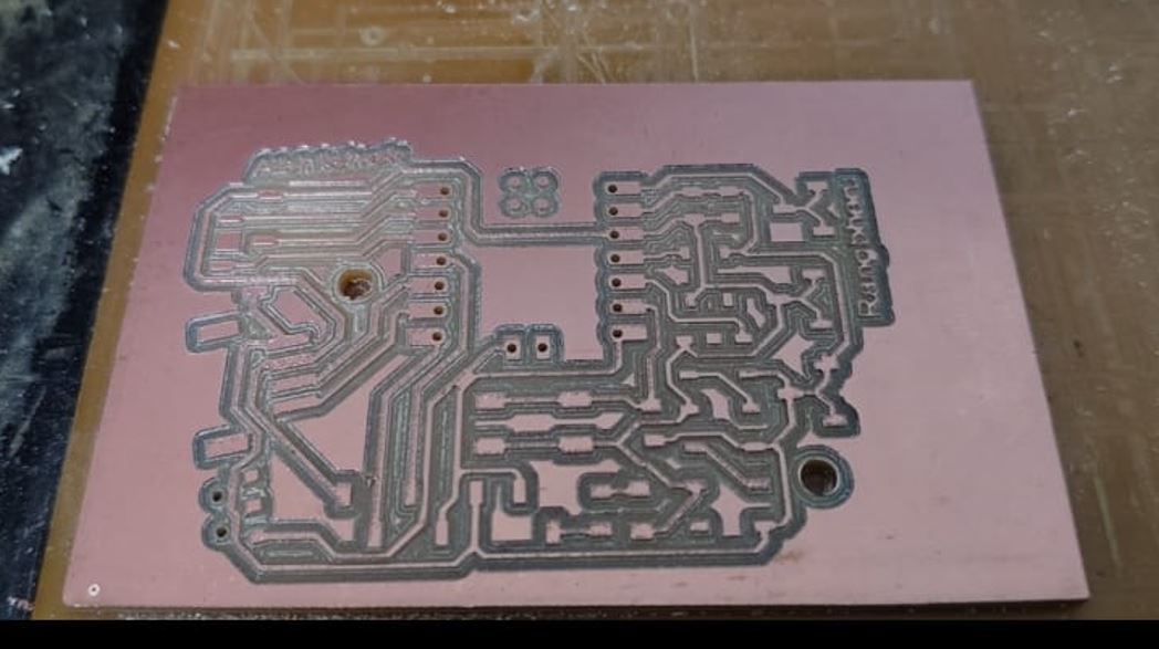
Now in below image, we can see that the End mill bit moved to the entered location, but its x coordinate is exactly on the top of the edge of the PCB, thus I increased X distance from 4 mm to 6 mm, so that the milling start point / workpiece origin is set at x = 6 mm and y = 6 mm. It is very important to remember the origin point.
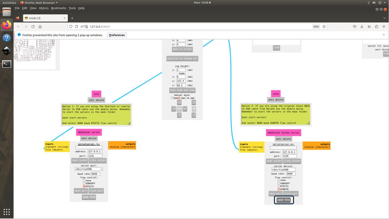
We can calculate and see the trace and tool path by clicking on the view button and finally click send the milling process will be started.
Milling the Drill Top Layer
Now I moved the bit to position to change bit because to perform drill operation on top layer, I need to use 1/32 (about 0.8 mm) drill bit.
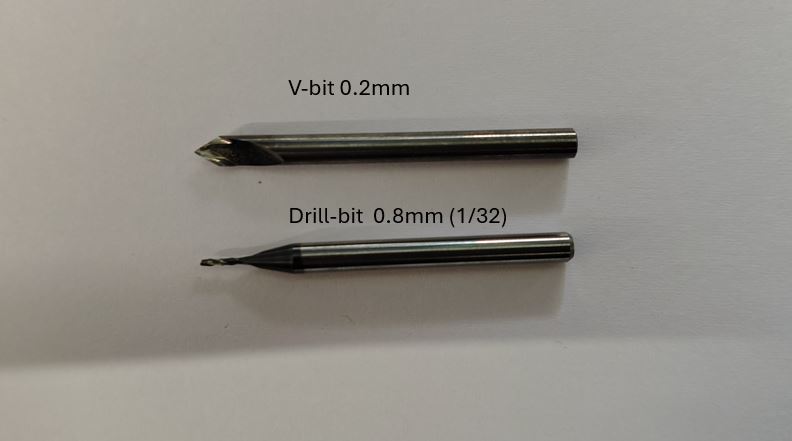
Now I uploaded the PNG of Drill Top Layer and selected the Drill Bit 1/32 in the modes and then calculated the toolpath move the bit to origin and send the path to the Machine to start the Drilling process.
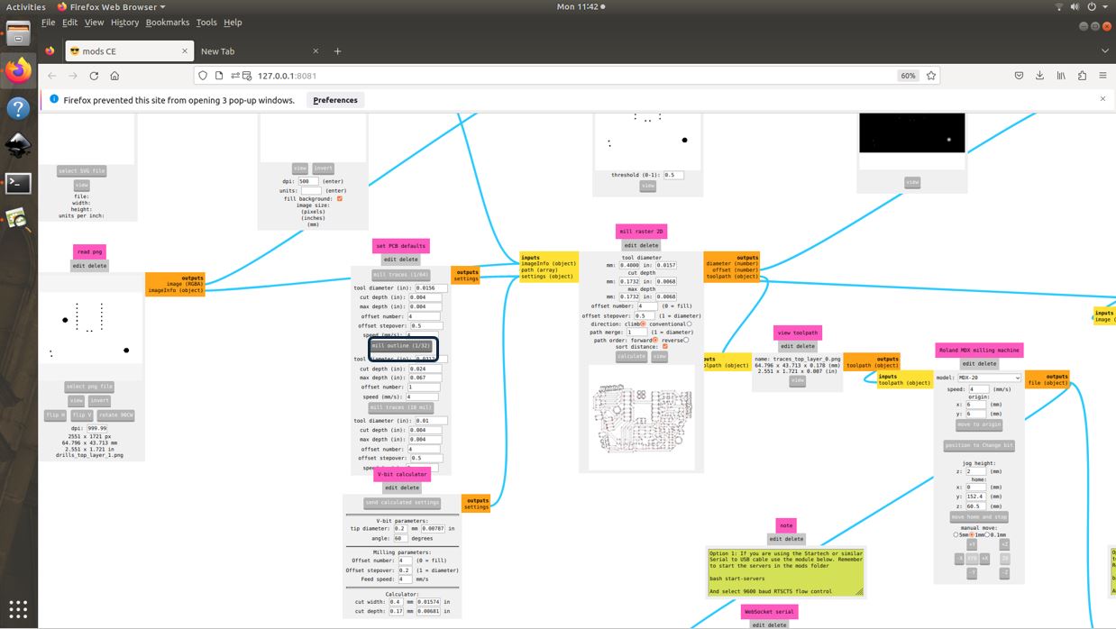
I sent the file to Machine and it started the drill operation.
Milling the Outline Top layer
This operation will be perform my drill bit do I do not need to change the bit, I uploaded the PNG of Outline Top layer and keep the Drill Bit 1/32 as it is in the modes and then calculated the toolpath move the bit to origin and send the path to the Machine to start the Outline cutting process.
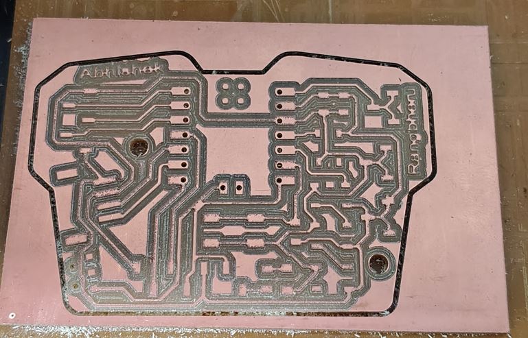
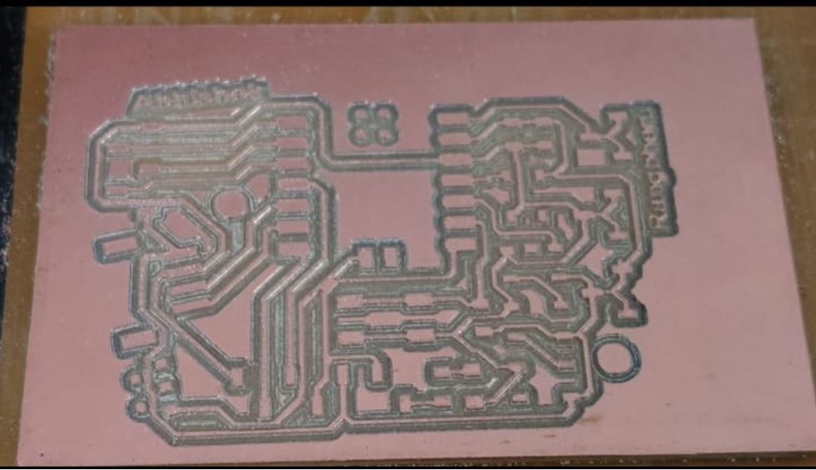
Then I used the scraper tool to take the PCB out from the bed.
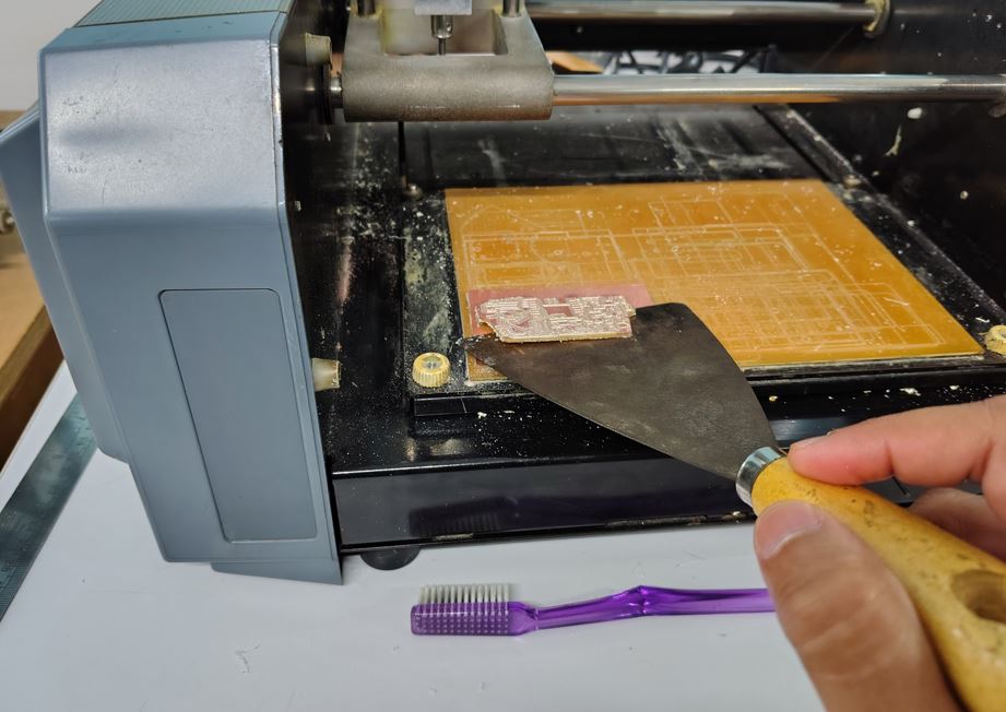
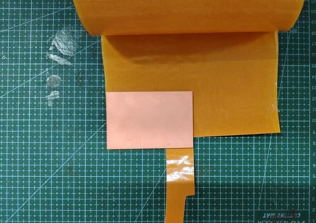
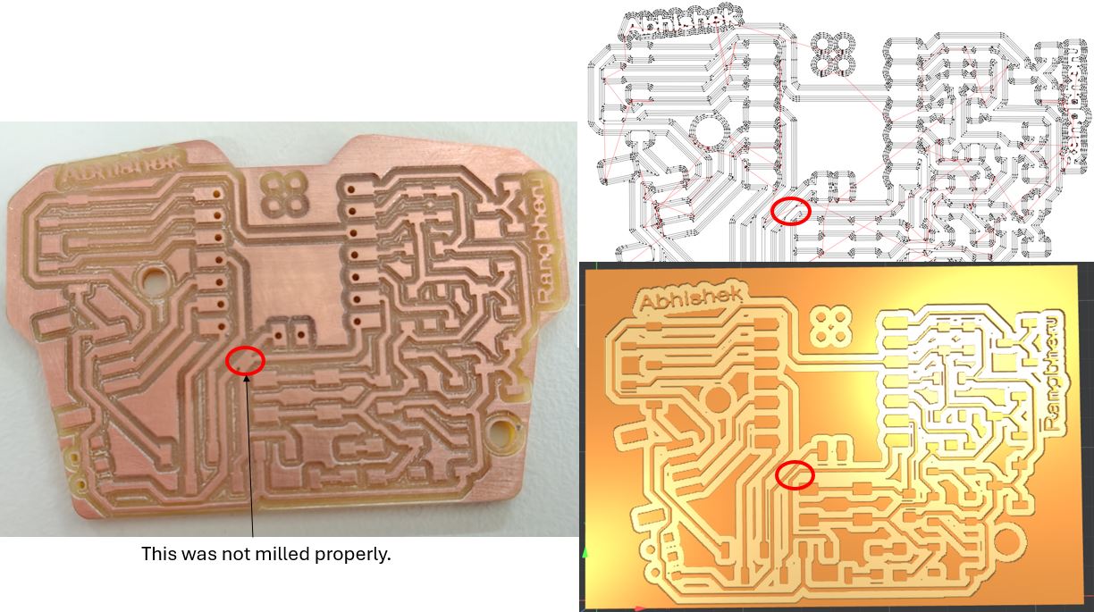
I used the cutter knife to remove the copper and separate the traces. They were not connected in 2D vector file and 3D File, however the actual PCB was having joint traces.
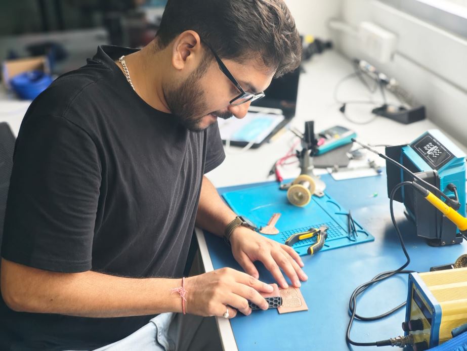
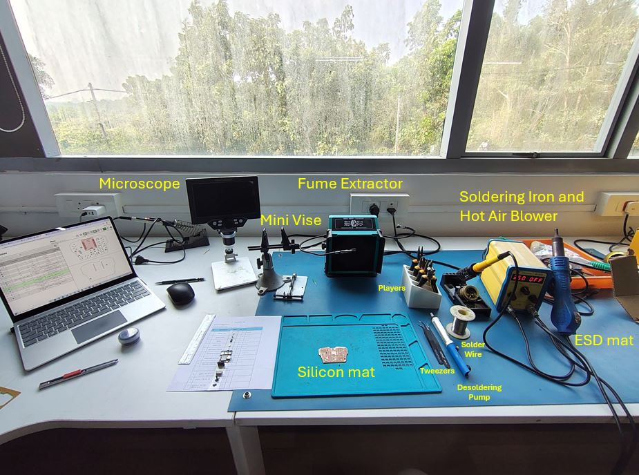
Component Soldering / Assembling
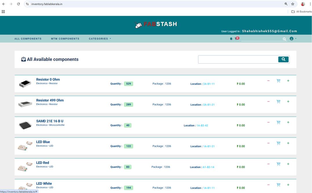
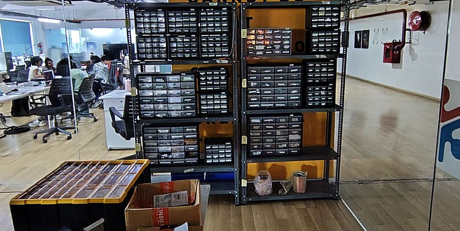
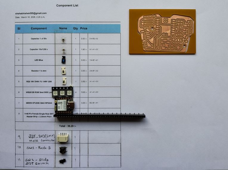
Using the FABSTACH, viewed and add the components from our FABLAB inventory. I printed the component list and used the double side transparent tap to stick the components on it.
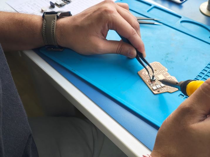
Here, while soldering the interactive HTML BOM is very useful to locate the component placement, and orientation mark it placed after soldering. The hovering feature over list can help locate the components.
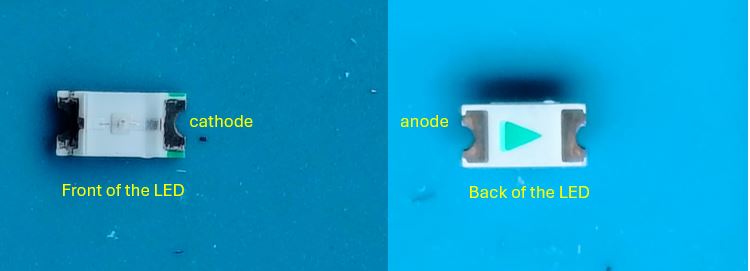
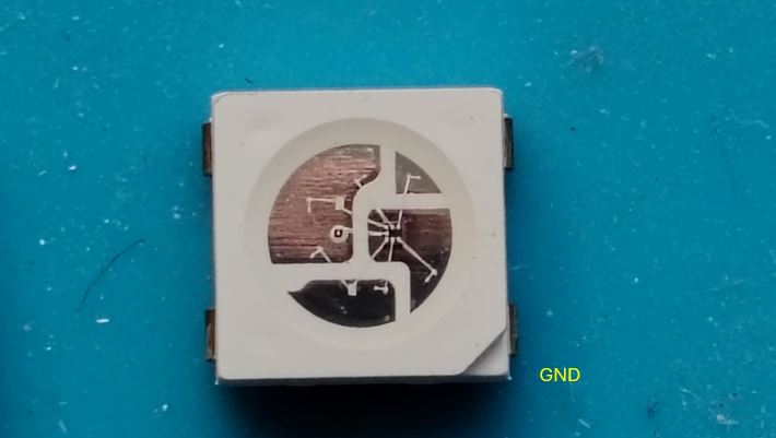
Understanding the direction of polar components such LED is important. In below image the direction of green aero shows the anode or the green lines on the top shows the cathode of the LED.
While soldering SMB components, always heat the pad first then touch the solder wire to the pad not to the soldering iron. Then place the component using tweezers and heat the pad/component leg so that they will get connected. Now the component is placed properly aligned with other remaining pads. I soldered the remaining pads with the component legs.
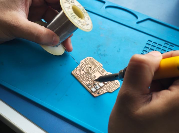
Another important thing is to solder small and tiny component first and solder the big and the tall component in the last. Following this I soldered all the components of my board.
Inspection and Testing
The first thing that, I did was to clean the PCB with the pcb cleaning isopropyl alcohol.
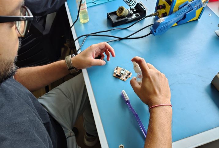
Then, I used the multimeter to Test the continuity for any short circuit or open connection, It is good to refer the schematics and Gerber file while doing continuity test. I also checked the continuity from each XIAO EXP32C6 Pin to the Female Socket header using jumper wire.
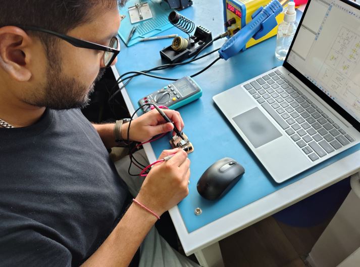
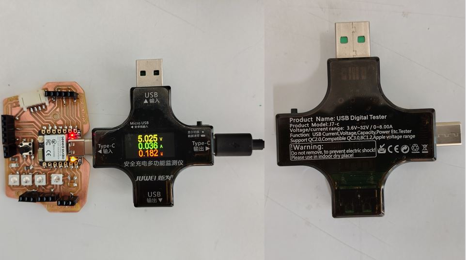
Last, I tested with USB Digital Tester (Model : J7-C) to check the Power on current consumption.
Next, I tried to program and tired to Blink LED.
          const int BlueLED = D7;         // the Pin number of Blue LED pin

          void setup() {
            // initialize digital pin BlueLED as an output.
            pinMode(BlueLED, OUTPUT);
          }

          // the loop function runs over and over again forever
          void loop() {
            digitalWrite(BlueLED, LOW);      // change state of the LED to LOW level
            delay(100);                      // wait for a 0.1 second
            digitalWrite(BlueLED, HIGH);     // change state of the LED to HIGH level
            delay(100);                      // wait for a 0.1 second
            digitalWrite(BlueLED, LOW);      // change state of the LED to LOW level
            delay(100);                      // wait for a 0.1 second
            digitalWrite(BlueLED, HIGH);     // change state of the LED to HIGH level
            delay(700);                      // wait for a 0.7 second
          }
Last, I tried to program the Push_Button and tired to Blink LED based on Push button Input.
          const int BlueLED = D7;         // the Pin number of Blue LED pin
          const int PushButton = D8;      // the number of PushB Button pin,
          int ButtonStatus = LOW;         // Variable for reading the pushbutton status
          int i;                          // counter for for loop

          void setup() {
            // initialize digital pin BlueLED as an output.
            pinMode(BlueLED, OUTPUT);
            pinMode(PushButton, INPUT);
          }

          // the loop function runs over and over again forever
          void loop() {
            ButtonStatus = digitalRead(PushButton);   //read the digital status of Push Button

            if (ButtonStatus == HIGH)                  //if Push Button Status in HIGH then flash LED
            {
              for (i = 0; i<10; i++)
              {
                digitalWrite(BlueLED, LOW);      // change state of the LED to LOW level
                delay(100);                      // wait for a 0.1 second
                digitalWrite(BlueLED, HIGH);     // change state of the LED to HIGH level
                delay(100);                      // wait for a 0.1 second
                digitalWrite(BlueLED, LOW);      // change state of the LED to LOW level
                delay(100);                      // wait for a 0.1 second
                digitalWrite(BlueLED, HIGH);     // change state of the LED to HIGH level
                delay(700);                      // wait for a 0.7 second
              }
            }
            else
            {
              digitalWrite(BlueLED, HIGH);        // change state of the LED to HIGH level
            }
          }
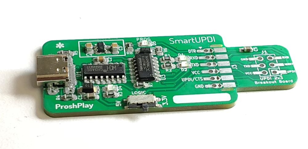
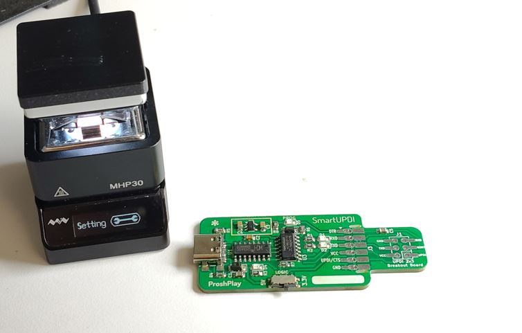
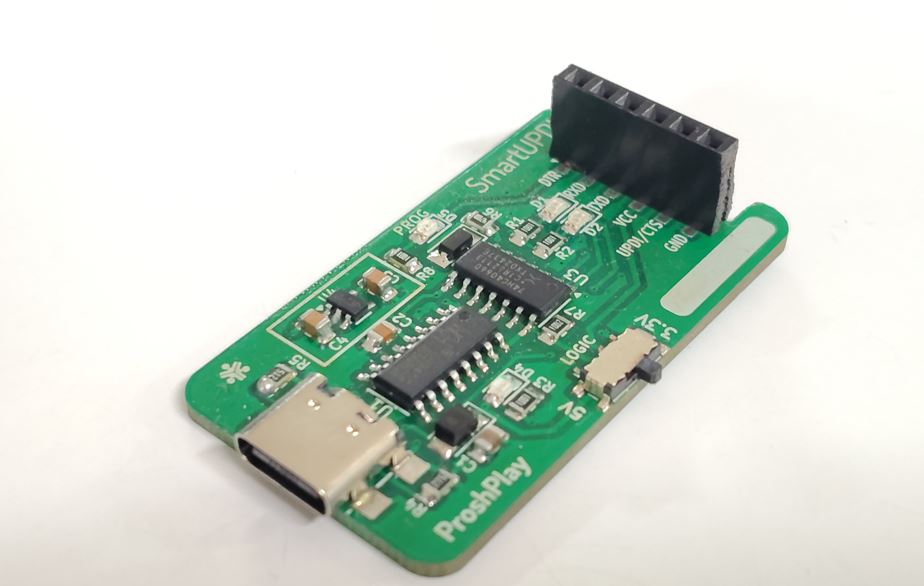
SmartUPDI - Hot Plate Soldering
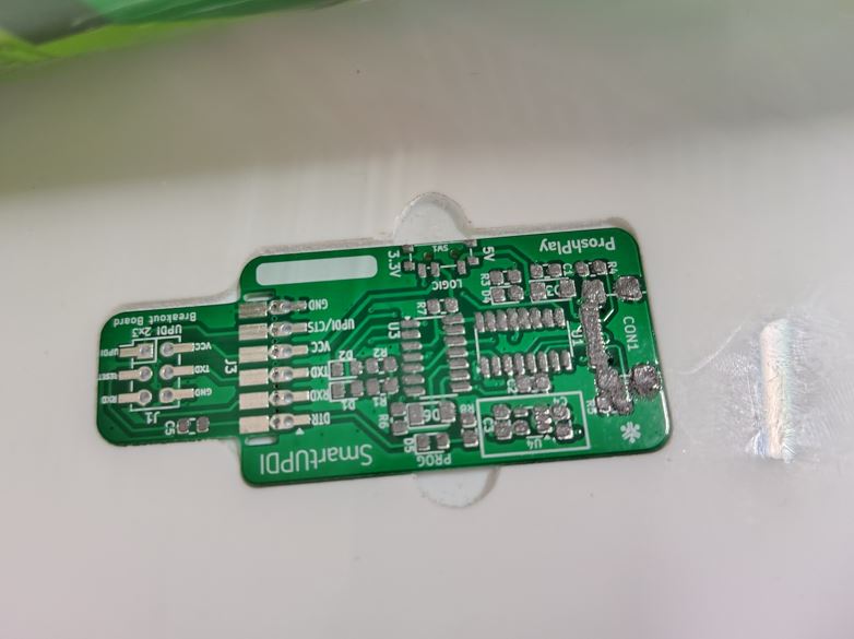
As a group, we sent a Smart-UPDI Programer to vender to get printed circuit board. After receiving it a few weeks later we used a new process to solder it using Hot Plate Preheater.
First, we need to 3D printed cavity bed to place he PCB and then laser cut a foil (in our case we cut the mountain due's circler sheet). Laser cut with the top layer of soldering pads.
Second, Place the PCB on the 3D printed bed and match the sheet's cuts with the PCB pads and then apply soldering paste. Apply optimal past more paste will bump/bounce the SMD components while heating.
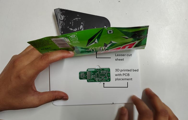
Third, I placed the SMD components on the PCB. It will stick with the soldering paste.
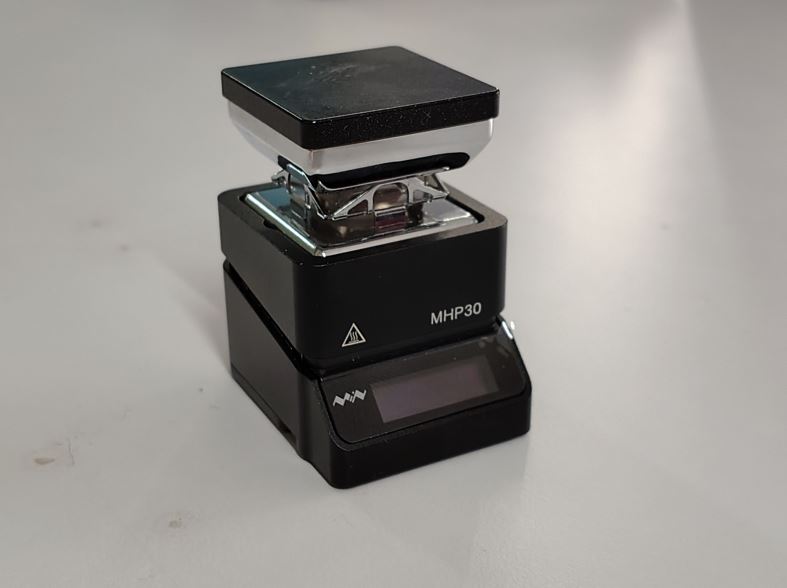
Forth, we turned on Miniware MHP30 Hot Plate Preheater and set the temp around 180 °C to 200 °C and thenm placed the PCB on the heating bed and slowly move the PCB so that all the area of PCB gets heated and soldering paste gets melted and comonents get soldered.
What Went Wrong
We can see in the below video at 0.01s the resister came flying and at 0.07s the capacitor stand-up!
My instructor Mr. Saheen stepped in and corrected the placement of the resistor and capacitor.
What I Learned
Make sure we apply optimal thin layer of soldering paste the excess paste will result as above.
  // ATtiny1624 LED Blink
  // LED connected to PA5 — Active High (LED ON when pin is HIGH)

  #define LED_PIN  PIN_PA5    // define PA5 as the LED pin
                              // PIN_PA5 is the Arduino-style name for PA5 on ATtiny1624

  void setup() {
    pinMode(LED_PIN, OUTPUT);     // set PA5 as output — allows us to drive current through LED
    digitalWrite(LED_PIN, LOW);   // start with LED off — ensure known state at power up
  }

  void loop() {
    digitalWrite(LED_PIN, HIGH);  // set PA5 HIGH — LED turns ON (Active High)
    delay(500);                   // wait 500ms — LED stays ON for 0.5 seconds

    digitalWrite(LED_PIN, LOW);   // set PA5 LOW — LED turns OFF
    delay(500);                   // wait 500ms — LED stays OFF for 0.5 seconds
                                  // loop repeats forever — continuous blink
  }


  //**Before uploading, make sure these settings are correct in Arduino IDE:**

  //Go to `Tools` and verify:
  //- Board: `ATtiny1624`
  //- Programmer: whatever you are using (UPDI programmer — e.g. `SerialUPDI` or `jtag2updi`)
  //- Clock: `Internal 20MHz` (or whatever you have fused)

  //**Also make sure** you have the **megaTinyCore** board package installed — that is what provides `PIN_PA5` and ATtiny1624 support. In Arduino IDE go to `File → Preferences → Additional Board Manager URLs` and add:
Downloads and references
Key Learnings This Week
- Order of component soldering --> Low - High / Smallest to biggest
- Remove small islands.
- Sand just before soldering and clean with IP.
- Use 0.3mm solder wire best.
Reflection
I shall document everyday because if I don't do it then Tuesdays and Wednesdays becomes very stressful. and I cannot do extra things to bring my week's work to satisfactory ending. This week was the week when I shall 3D printed my case however I was not able to do so!!