INTRODUCTION
Another special week for me on my Fab Academy journey. If you've been following along, you know that I'm studying abroad in both Peru and Japan for the duration of the program, with 3 months in each. While living abroad is super amazing and I'm having the best time, I'm also living abroad without my dear and amazing wife. This week, my wife and her family are coming all the way from Canada to come visit me (and some of our family in Hokkaido) for 2 weeks!

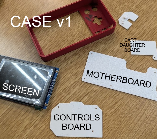
Although the list of goals just below looks short, this week was a lot of heavy lifting - and I had to pull the trigger on some major decisions for the development of my final project, the PAK. Follow along just below...
[x] Define and apply system integration to your final project
STARTING SPIRAL 3
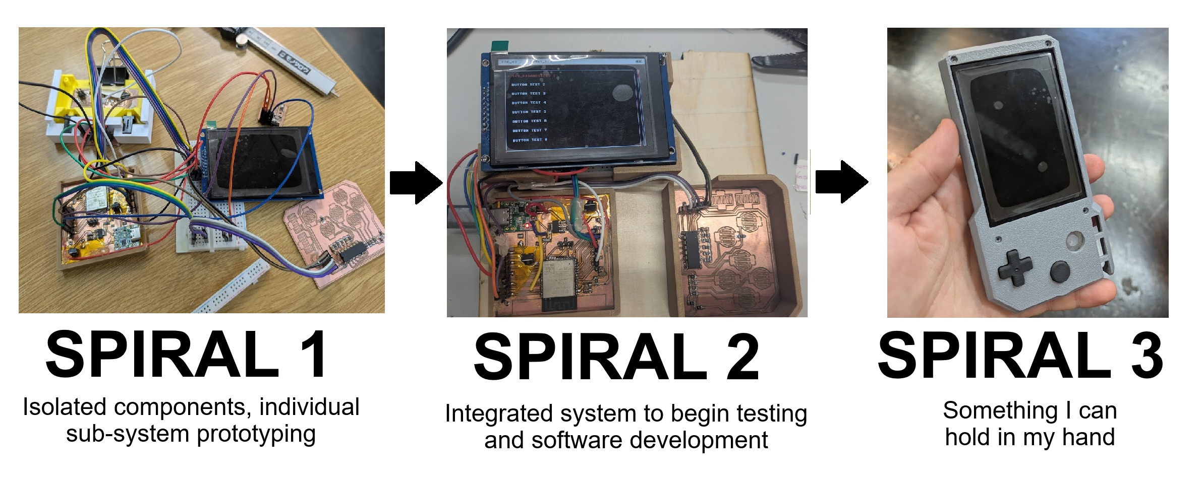
I decided that this week would be where I use all I learned about the proof of concept DEV KIT that I've been working on over the last few weeks here in Yokohama and start production on what could (fingers crossed) be called the final version of the PAK (at least in terms of project presentation). I spent some time this week reformatting my final project page to better reflect the spirals and stages of my final project so far, including adding a LOT of documentation on the things I learned this week and in the previous weeks from tinkering with the DEV KIT. Early in the week, I made an ordinal list of priorities to continue development on the PAK:
- Finalize motherboard PCB and ship out to JLCPCB
- Finalize control board PCB and ship out to JLCPCB
- Model the next iteration of the cartridge PCB
- Cast the membrane for the buttons and the buttons themselves
- Model the two halves of the case and determine mounting points
Once the PCBs from JLCPCB arrive, we could then focus on assembling the first draft of the PAK and collect data on how we can improve. I made a new document in Obsidian to keep track of all my thoughts and observations throughout the week.
PCBs
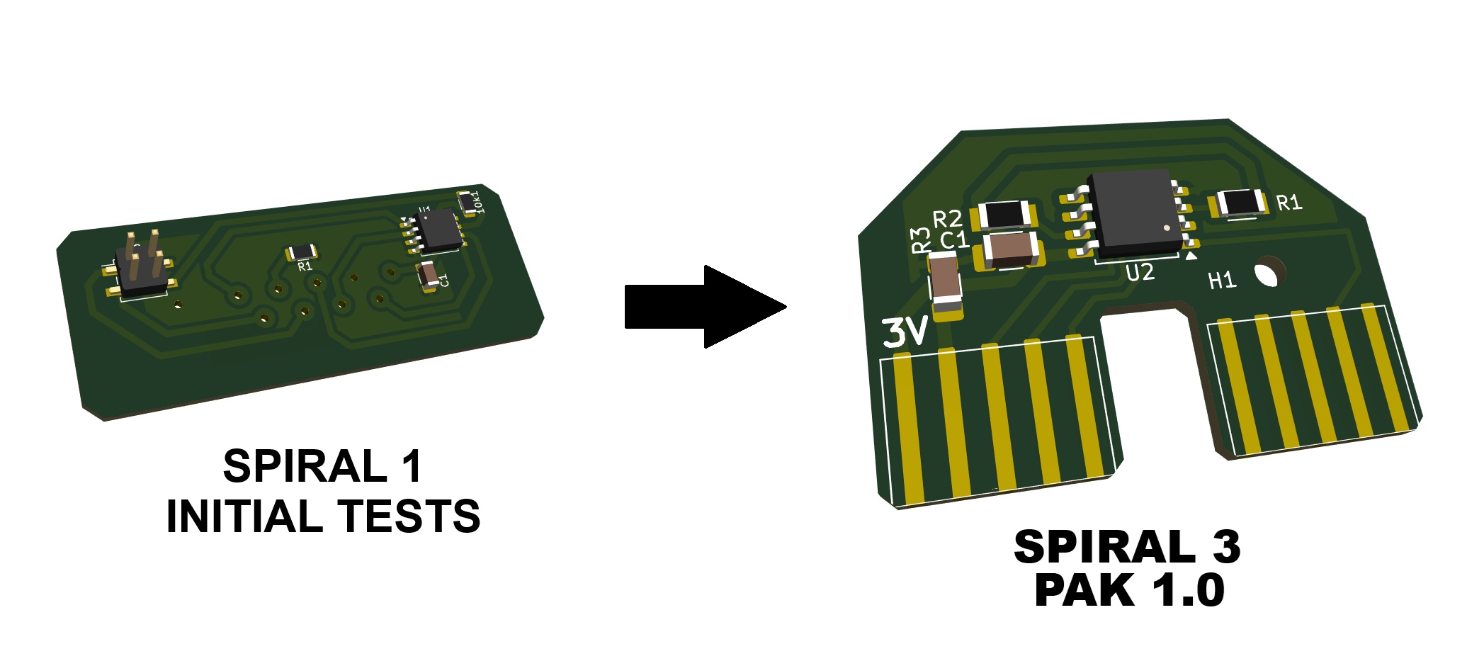
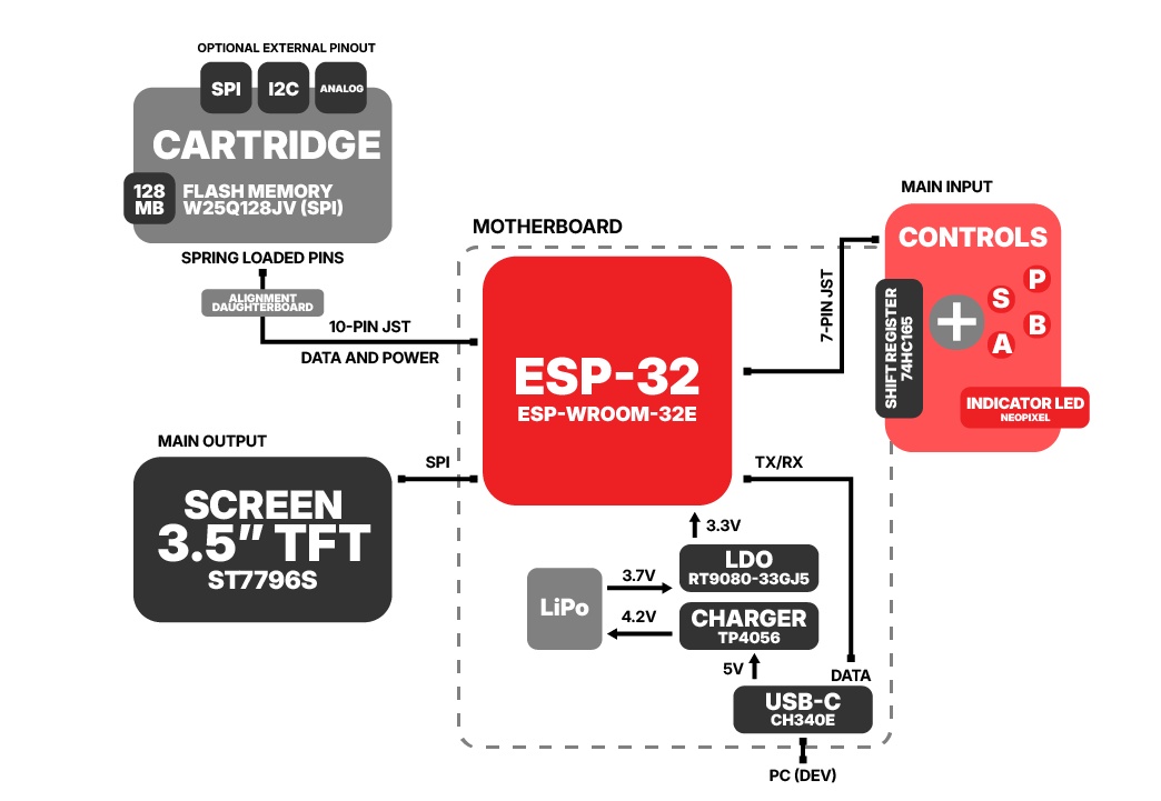
I've been agonizing over the idea of shipping out a PCB to a board house due to some unneeded perfectionism. A board could take anywhere up to a week (or even more) to arrive in the mail and my initial cost estimates put a shipment in at around $40-50. These were two constraints I had been nervous about committing to, but it cost me a lot of time over the last few weeks. This week I finally bit the bullet and got two very important boards, the main motherboard and the control board, shipped off to JLCPCB (which ended up being so much cheaper than PCBWay). I had prototyped these two boards already in house on FR1 copper boards, but there are two reasons why I needed to get these done in a board house: They were both double-sided boards and they had a lot of complex routing and custom footprints that needed the best precision. I learned that making complex in house is rewarding but incredibly risky. For my final project, I knew these boards would need that extra level of detail to make everything come together.
You can read about the exact changes to these boards over on my final project page. Here I've got a summary of the changes and what I decided to prioritize.
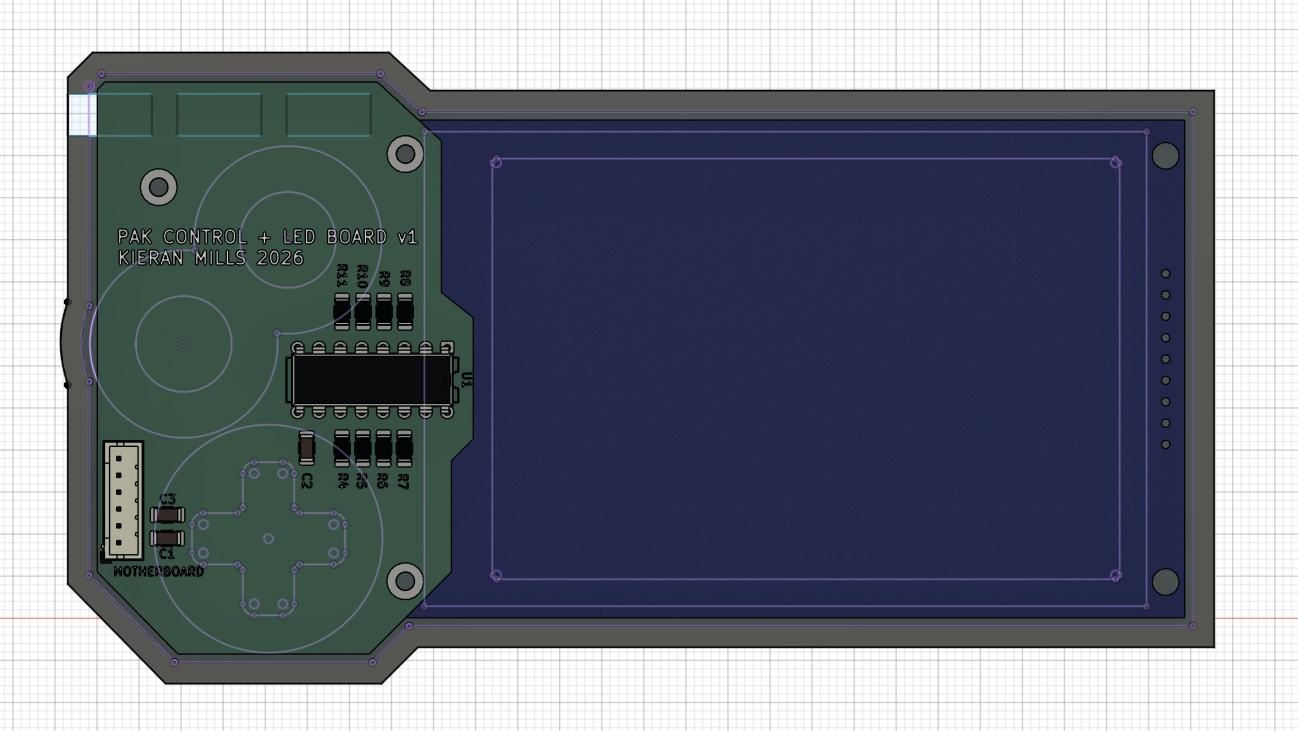
➔ Motherboard
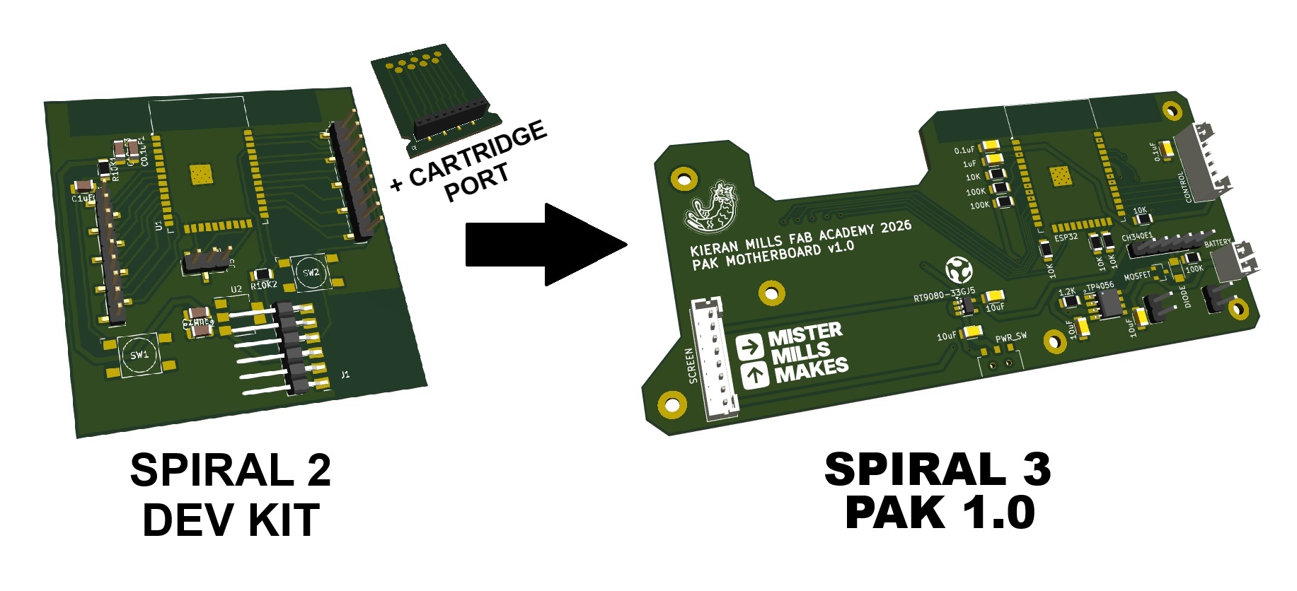
The idea behind this revision is to get as much of the final system hardware on this board as possible, while still prioritizing modularity for the components that need to be aligned within the final case. Also gone are the dupont headers that were so prone to breaking (also far too chunky and big for the final version) - replaced now with JST PH ports for easy but also low profile insertion. I did make a mistake here and ordered vertical JSTs which will cost me some Z height on the final design as a result, but my boards are actually small enough that I could place them in staggered formation - as I've placed the other headers on the bottom sides of the other boards! The extra width, as you've maybe noticed, is to finally accommodate the cartridge slot board - which has been an accessory board up until this point.
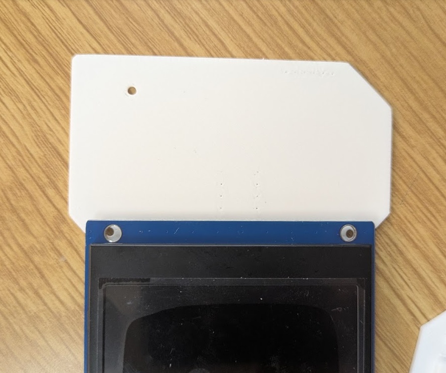
➔ Controls Board
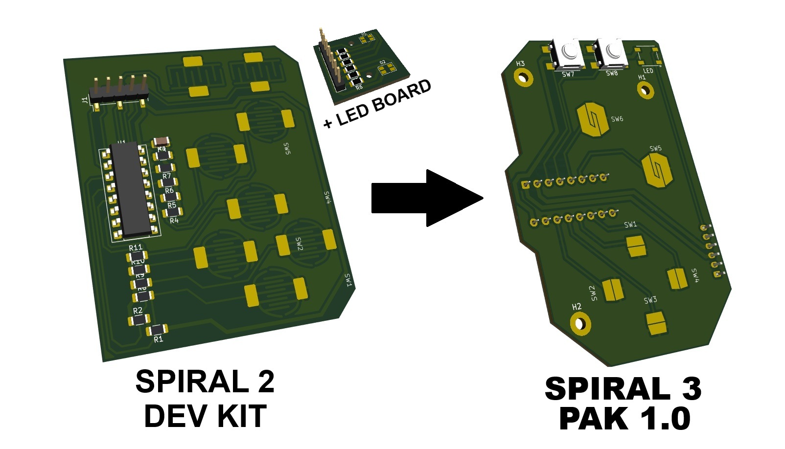
Not actually a lot of changes to this board other than the incorporation of the new (smaller) membrane pads that should be better thanks to JCLPCB's design constraints being more forgiving than our Genmitsu. Also included on this board is the
➔ Cartridge Board
Most notable of the upgrades this week is I've finally modelled a new cartridge board to utilize the new Bourns connectors I've sourced from DigiKey in place of the pogo pins I was experimenting back in the first spiral. I have been putting off redesigning this board until the parts arrived. I opted to add a notch and alignment key in this design to assist with the physical strain that the cartridge may undergo being inserted and removed over and over again. This board as well as the daughter board for the motherboard cartridge slot are milled in house as they don't require a lot of fancy tricks!
Lining Things Up in CAD
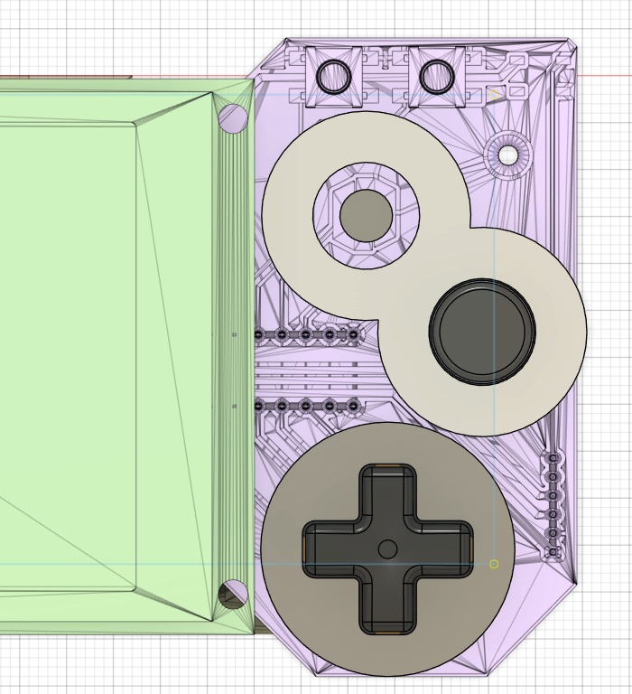
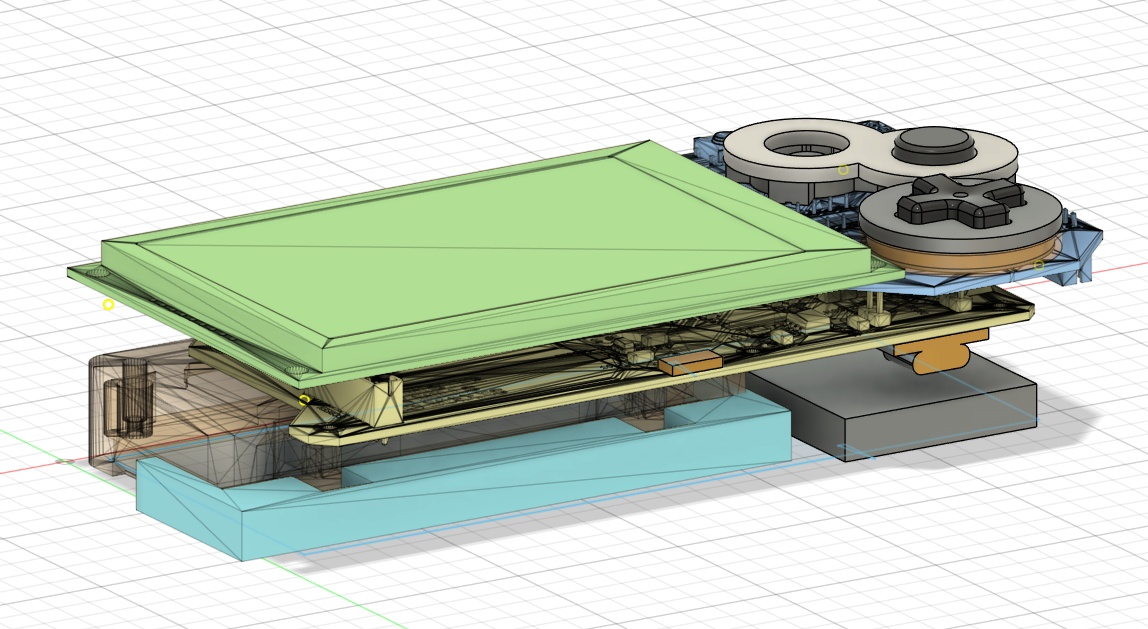
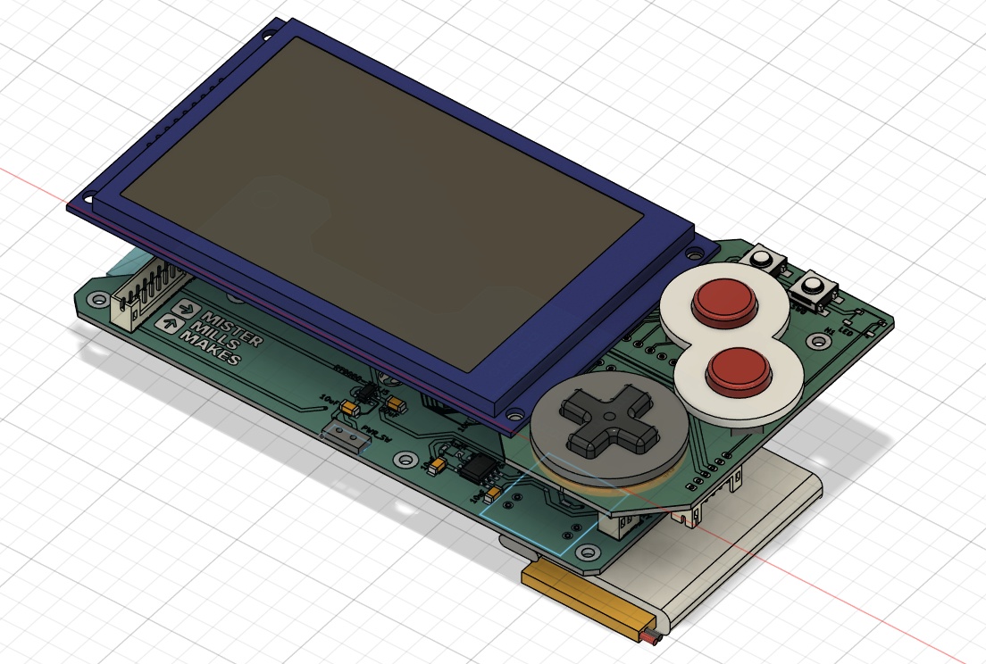
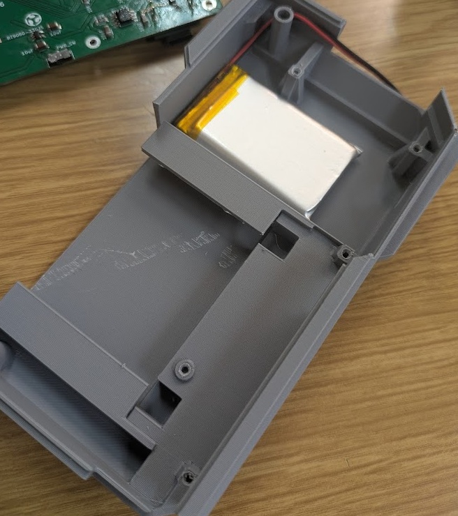
Now that we had the major design constraints finalized in the form of the PCBs, we could start laying things out in CAD and prepare the other components to fit nicely. I started by importing all of the components I had information about into a single Fusion file. This included the TFT screen (I previously modelled this back in Week 3), the motherboard, the control board (not pictured here finished, but the dimensions are included), the battery, the face buttons, and the cartridge mechanism system.
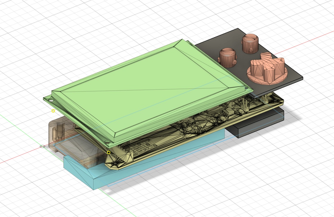
The result was quite messy but honestly, seeing the PAK in this configuration made things SO much easier to just start making decisions. I feel like making this virtual prototype cleared up so much of my choice paralysis because I could see what was going to work and what wouldn't by just moving things around.
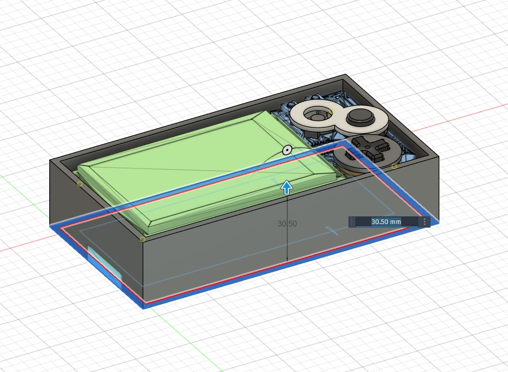
➔ 3D Printing PCBs
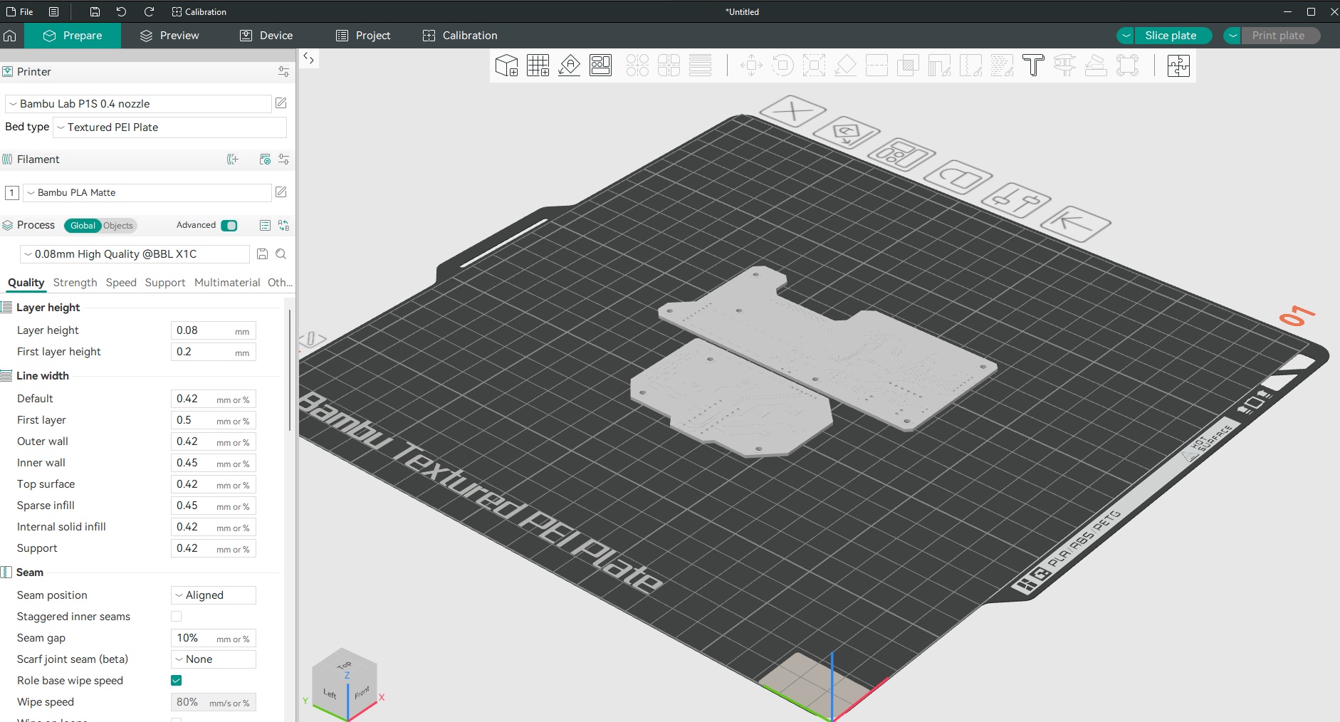
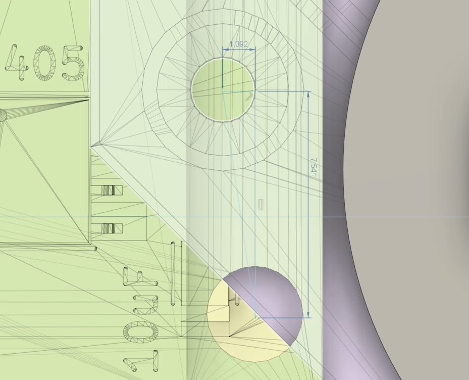
No, I'm not talking about making PCBs using the copper foil trick. I actually think it's a good idea for anyone making a complex multi-board enclosure device to print out your board footprints and just start playing with them in your hands to see how things feel.
This was especially helpful for me since my PCBs were still in transit from JLCPCB. I could get really important information about the final design, like if my screw holes line up (this one is a bit off) without needing the real boards in my hands.
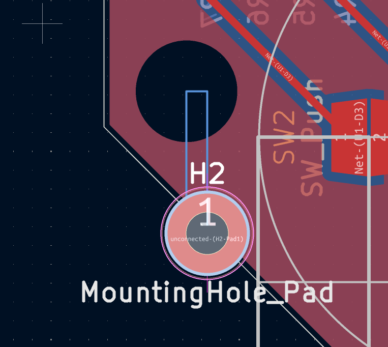
➔ Bosses
Most importantly, I was able to start thinking about where my fixtures would line up with the PCBs and TFT screen. I mention in my final project page that the design of the case is actually the lowest priority since I can rapidly prototype, so my strategy here was just to place as many mounting holes where space permitted and then hopefully I'd have enough places to secure everything. I know that doesn't sound super scientific, but it lets me get making and I can always iterate again later - and since my designs are parametric I can update locations of the plastic bosses easily!
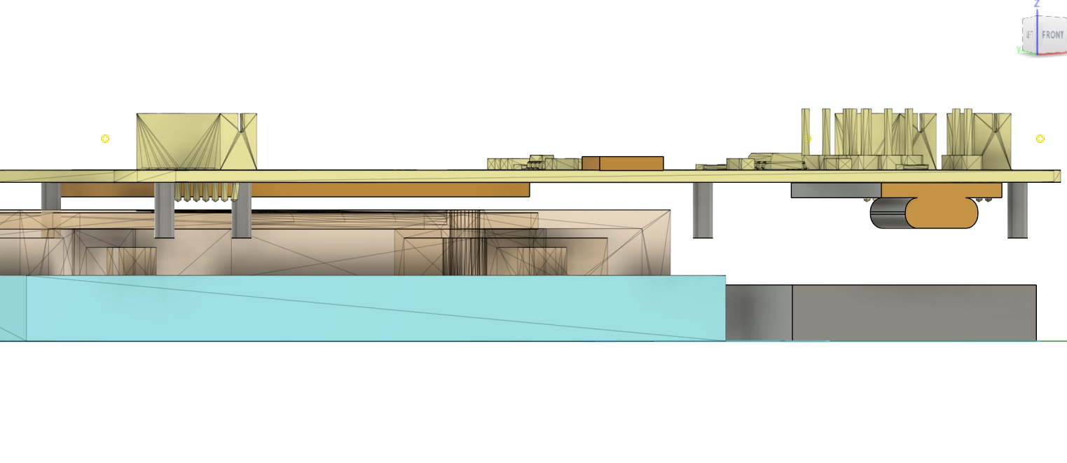
➔ Case
With a bit of a better draft layout, I could start developing a rough skeleton around the parts. It's always been the idea to have two halves of the case that come apart in the middle - for easy repairability and customizability of the top face plate.
Up until this point, I had been exporting STLs from KiCAD and importing them as meshes into Fusion, which always gave me this super ugly tesselated model in one colour. I didn't realize that the .STEP files you could export would have all of the colour data included AND the surface geometry editable!
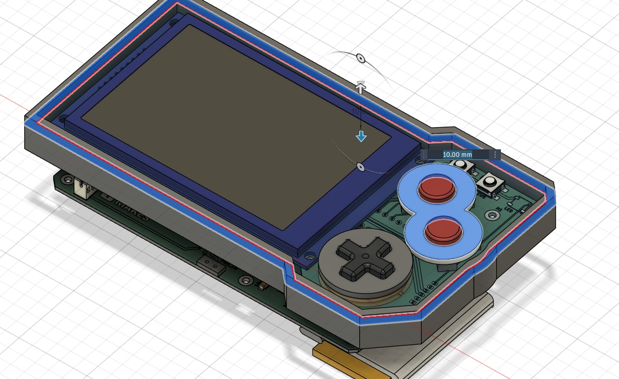
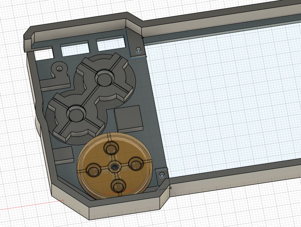
and the result - things actually fit so great! I slotted in some of the prototype buttons I was working on at the same time. Obviously colours not final but this is a great step towards a final version!
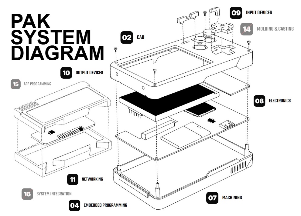
System Integration
Normally I don't directly answer the questions in my documentation that are provided on the assessment page for Nueval, but I felt it to be a bit more fitting given the content this week requires us to think ahead.
-
Have I made a plan for system integration for your final project?
Yes, I feel confident that I've broken down the remaining sub-systems into achievable chunks that I can complete each day. Notably, having a complete set of near final footprints that I can continue to rapidly iterate on is incredibly helpful for making progress -
Have I documented your plan with CAD and/or sketches for system integration?
Yes, I'm continuing to CAD the final case design with the completed footprints of the PCBs and other components, which is helping me very quickly get integrated designs that fit nicely -
Have I implemented methods of packaging?
The final packaging is split up into a top half and bottom half that can be iterated on separately, but I do need to design the mechanism that brings these two halves together. I would also like to experiment with other surface finishes for the top half to allow for "user customization" in the final version -
Have I designed your final project to look like a finished product?
This is one of the top priorities. Very excited to create something that could be "consumer-ready". Careful attention to surface finish and user interactivity (i.e. slide switch, USB port, etc.) are carefully considered. -
Have I documented system integration of your final project?
You're reading it :)
Again, you can follow along on the individual sub-system breakdown for the project on my final project page, but here we'll discuss some items to consider for the remaining time left in Fab Academy as it relates to system integration. Below is a living document of sorts to list the progress and my thoughts about what needs to be prioritized next in the coming weeks.
➔ Alignment
It's really important that everything in the final version of the device aligns nicely, and there aren't any bodged or forced connections. Things I've identified as potential issues:
- Cartridge click and alignment after the redesign
- JST connector height
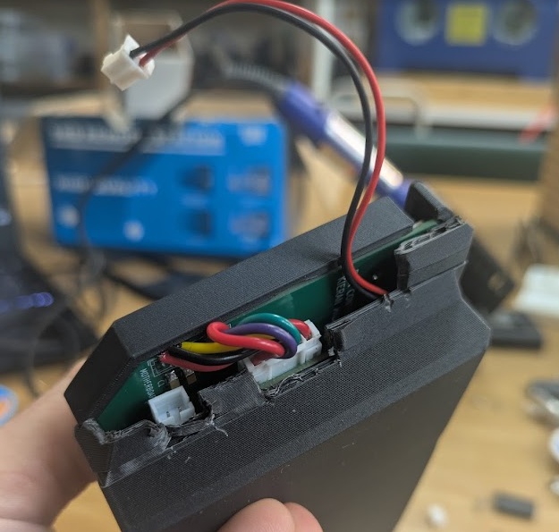
- Location and space occupied by the wires connecting each sub-board
- Screw bosses (I've only got M2x10mm and 6mm at the moment)
- Alignment of buttons with their membranes
- Alignment of the cartridge slot + daughter board + cartridge itself
➔ Stress Testing
In order to confidently survive the drop test, I need to think about ways of strengthening the PAK and ensuring the parts are secured. Some of the ideas I have either already implemented or plan to implement are:
- Screw/bosses wherever a hole permits
- Internal "raised" plastic to support boards
- Back stop for cartridge board and USB-C port board to handle the pushing and pulling force
- Wall thickness - we want to ensure we're not going too thin in places and also not overprinting in places we can afford to make thinner
➔ Aesthetics + Feel
The look of the device is of course secondary to the function, but it has been a major goal of mine for this program to design with intent and create something truly pretty, so I'm thinking about the following as I continue to integrate the remaining sub-systems:
- The colour of the materials used (plastic case, buttons)
- Bevels and chamfers - don't go overboard but I would love to get closer to that gunpla look
- The open flat space created by the chin of the TFT screen near the control board