Week 8 : Electronics Production
Group Assignment
- characterize the design rules for your in house PCB production process
- submit a PCB design to a board house
Individual assignment:
- make and test an embedded microcontroller system that you designed
- extra credit: make it with another process
Learning Outcomes
- Design a functional embedded system from schematic to PCB layout.
- Generate manufacturing files and prepare a design for professional fabrication.
- Test and debug a custom PCB to ensure it meets the intended requirements.
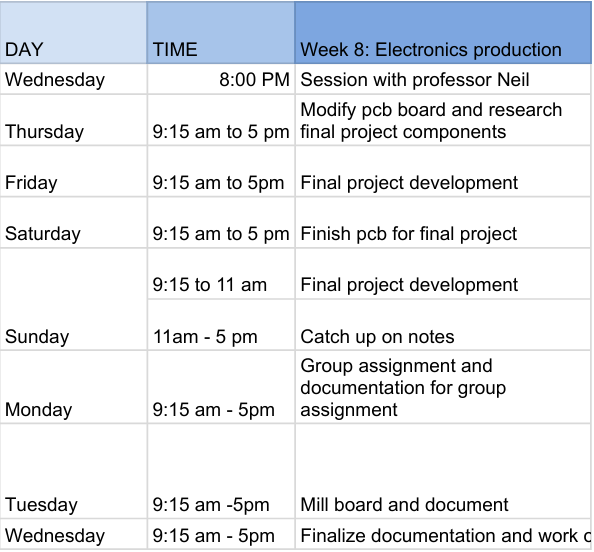
For this week, this is my schedule:
Group Assignment:
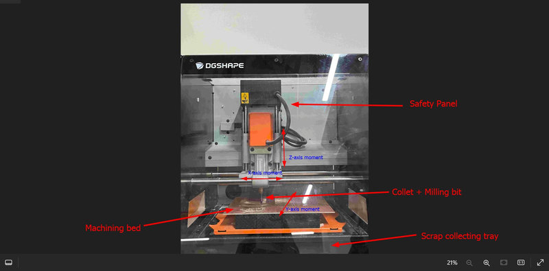
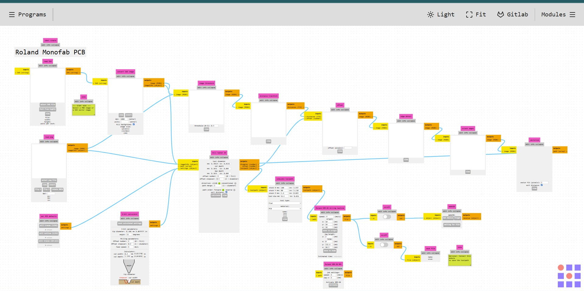
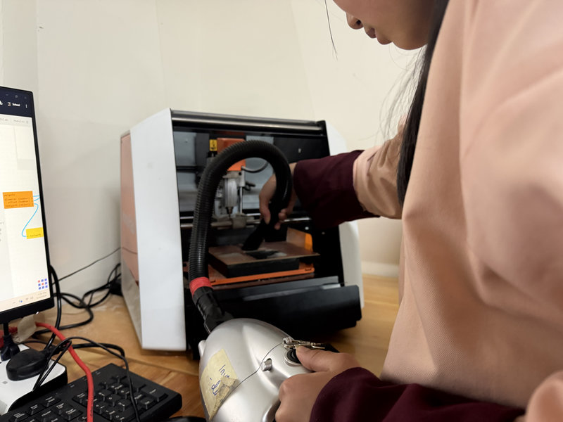
The Monofab SRM 20 Milling Machine
The Roland DGSHAPE MonoFab SRM-20 is a compact desktop CNC milling machine.It operates on 3 axes (X, Y, and Z) which allows it to mill precise shapes and patterns onto different surfaces.

This machine is one of the most widely used pieces of equipment in Fab Labs around the world, and it is the one we use in our lab for all of our PCB milling. The SRM-20 is capable of working with a wide range of materials including wood, foam, acrylic, and soft metals. However, for our Fab Academy assignments we primarily use it with copper clad PCB boards for producing our actual circuit boards.Despite being a relatively small and affordable machine, it consistently produces accurate and clean results.
I got this labelled image of the SRM-20 from Azhim Damzang's Week 4 page.
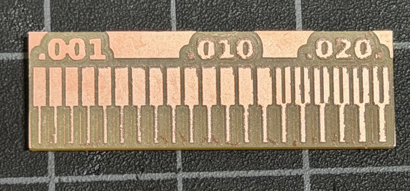
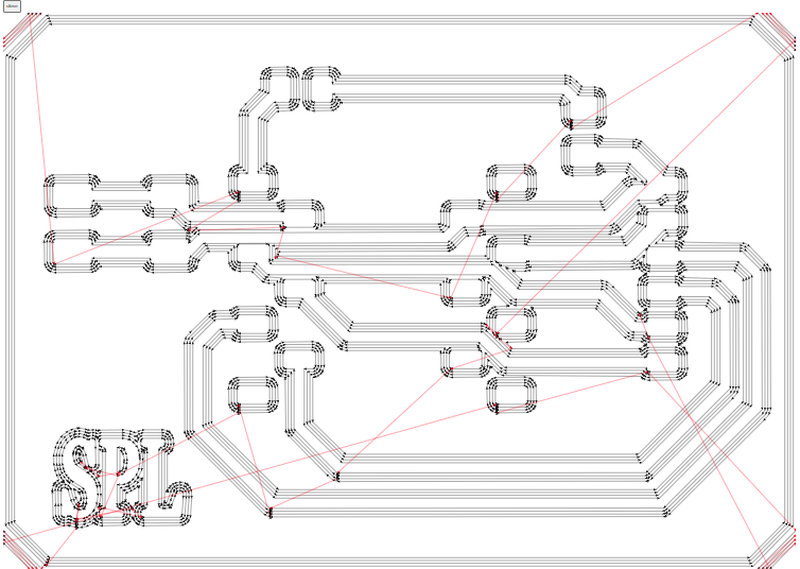
For our group assignment, we began by downloading the PNG test images directly from the Fab Academy website. These images are specifically designed to test different trace widths and spacings to help us figure out the minimum dimensions we can reliably mill on our PCB milling machine.


We used a 1/64 inch milling bit to mill the traces onto the copper board.
After carefully examining the milled results up close, we made an important observation that the traces and their spacing only came out clean and clearly defined starting from the 0.020 inch setting. Anything smaller than that was either too thin or not properly separated from the neighboring traces. The reason for this comes down to the bit size itself — since the 1/64 inch bit has a diameter of 0.015 inches, it can only cleanly cut spaces that are larger than that diameter. This means that 0.020 inches is the smallest reliable trace width and spacing we can work with, since it is the first size in the test array that exceeds the bit's own diameter.
You can access our group assignment here.
Individual assignment
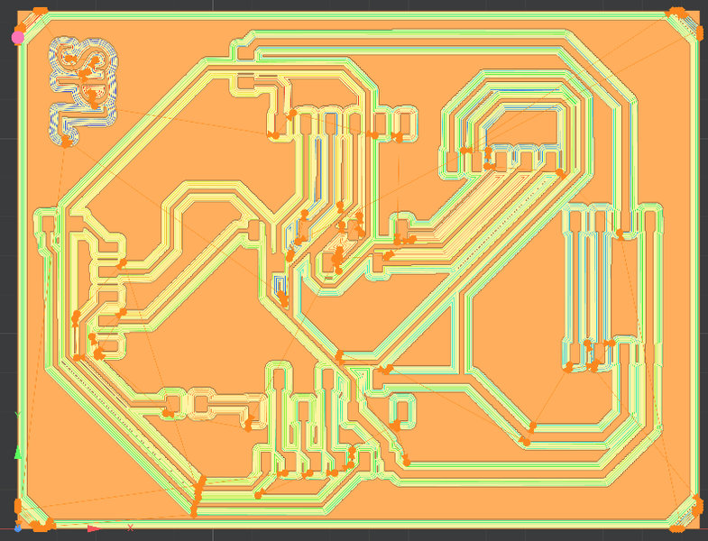
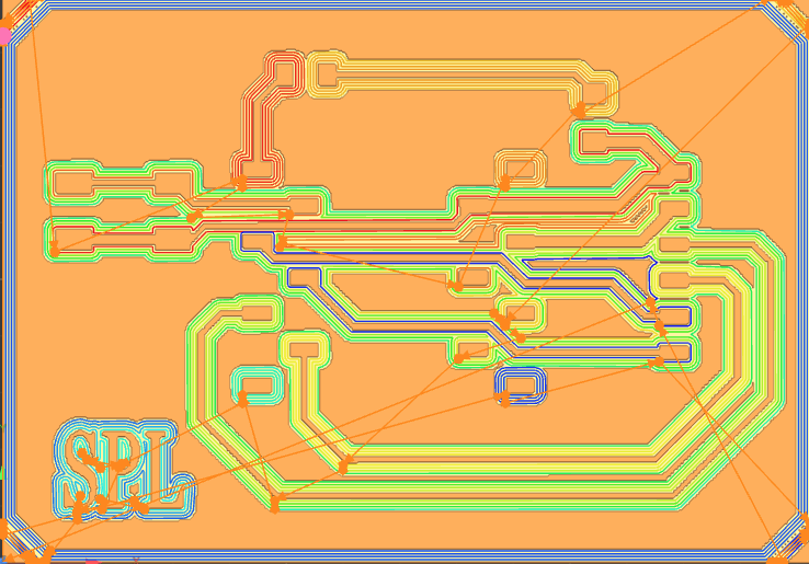
For this week’s assignment, which involved creating and testing a self-designed embedded microcontroller system, I chose to test the board I had developed for my final project during the electronics design week. However, I needed to make some additional modifications, as a few of the components required changes.
.jpg)
The modified PCB:
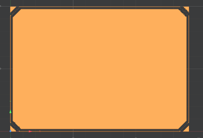
Adding Edge Cuts
Edge cuts are the lines that define the outer shape and boundary of a PCB, showing where the board will be cut during fabrication.To add an edge cut layer to your PCB, change the active layer from F.Cu to Edge.Cuts
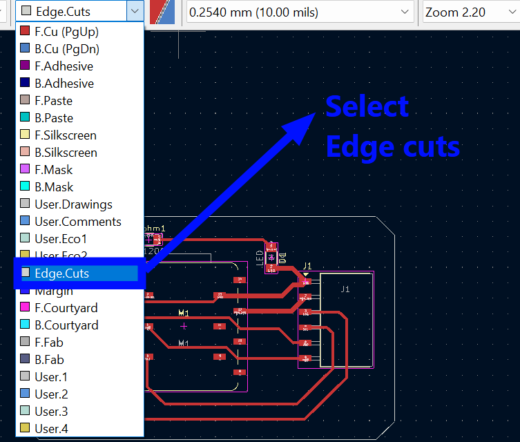
To draw the edge cuts, you can use lines to create a custom shape, or select the rectangle tool from the tools section to draw a defined border.I chose the rectangle for my pcb and make sure it's 0.6mm

To smooth the sharp corners of the board, I also chamfered the edges by right clicking on the border, selecting Shape Modifications>Chamfer Line, and setting the radius to 3 mm.
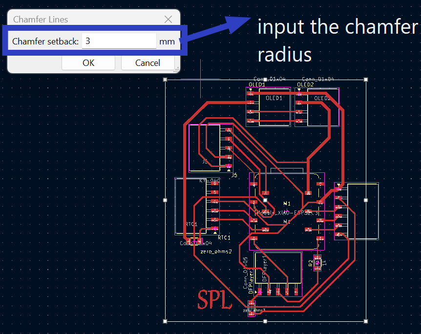
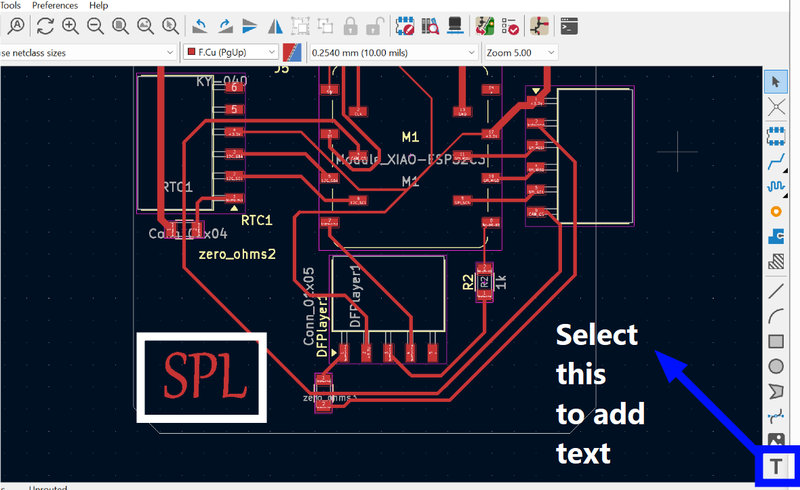
I added my initials on the baord using the Text tool in Kicad. Just press the 'T' icon on the left tool panel near the image tool.
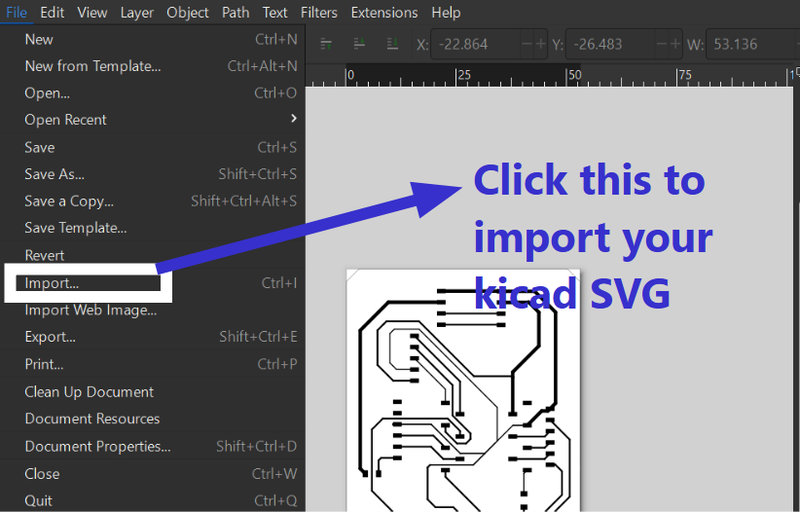
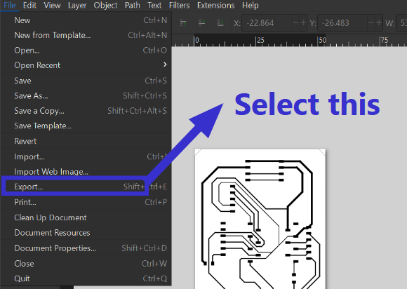
Exporting PCB from kicad
To export your design from KiCad as an SVG file, go to **File>Plot** and then configure the following settings:
.jpg)
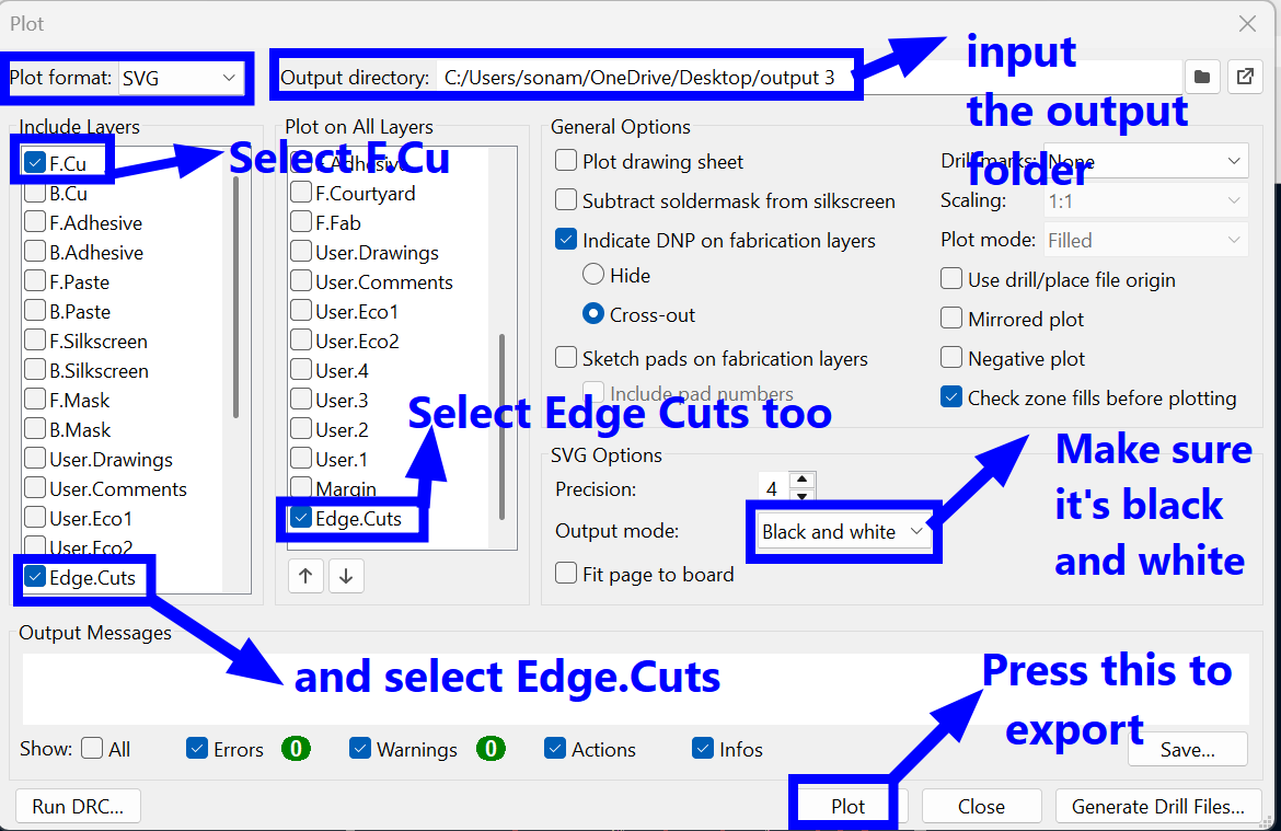
Plot format: Select SVG from the dropdown menu.
Output directory: Click the folder icon to choose where your files will be saved.
Include Layers:
- For the Traces:Select F.Cu.
- For the Outline:Select Edge.Cuts.
SVG Options:
- Output mode: Change this to Black and white. This is important for the milling software to recognize the paths correctly.
- Precision: 4 is standard.
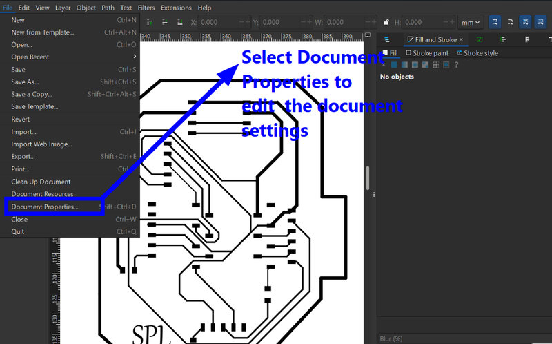
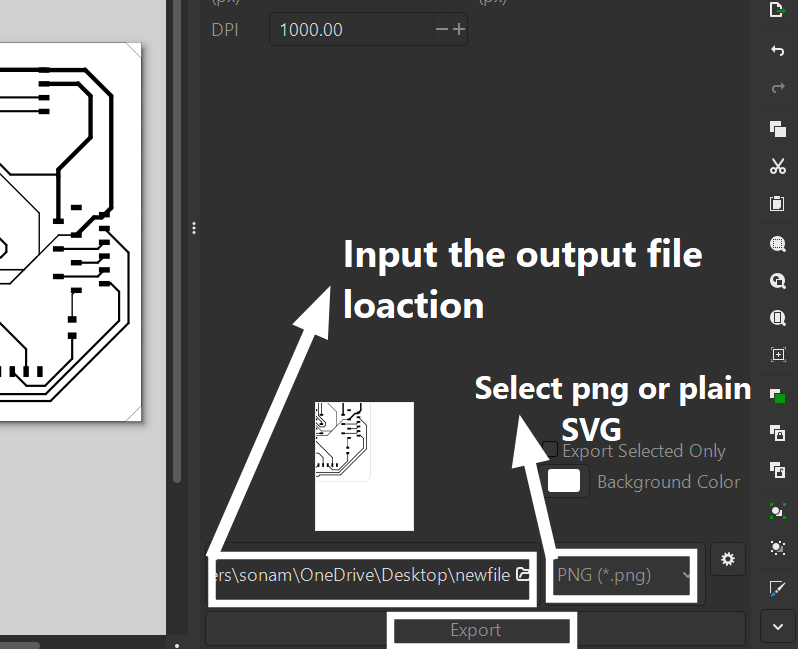
- Before bringing your PCB files into MODS, they must first be converted into the proper format. Start by opening Inkscape and importing your exported PCB file through File > Import, then select your file.
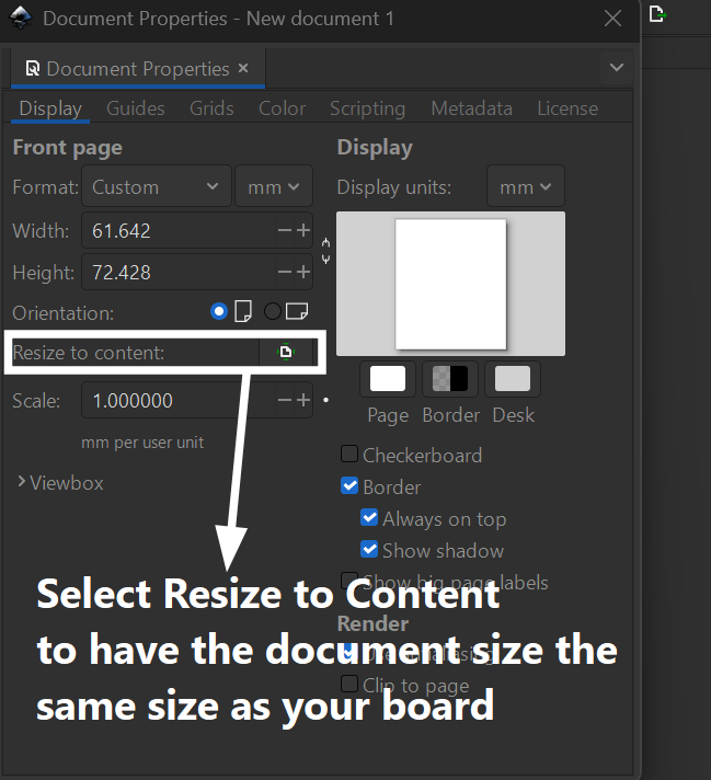
- The imported image might appear smaller than expected on the canvas. To adjust this, go to File > Document Properties and choose Resize to Content (or press Ctrl+Shift+R) so the canvas fits the image. Avoid scaling the actual design, as its dimensions are already correct from the PCB export.
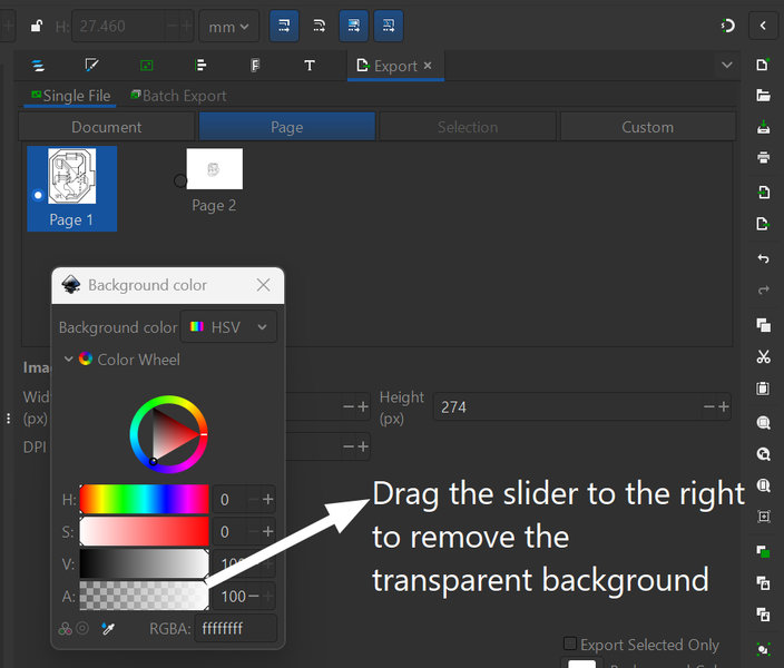
- Ensure the background is not transparent.Set it to white in the Document Properties, so the image displays correctly in MODS.
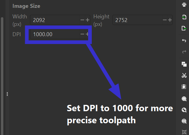
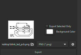
- Once everything appears correct, go to File > Export and select PNG as the format. Set the DPI to 1000 to achieve high resolution output, which helps MODS generate precise toolpaths.
Generating RML file
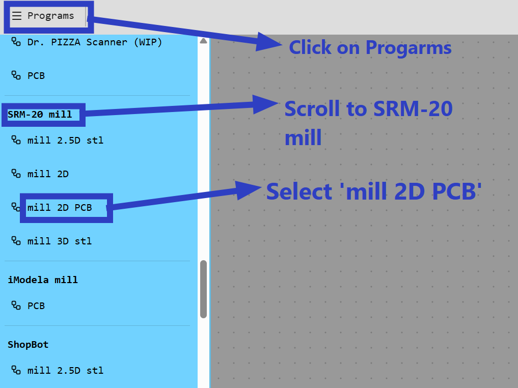
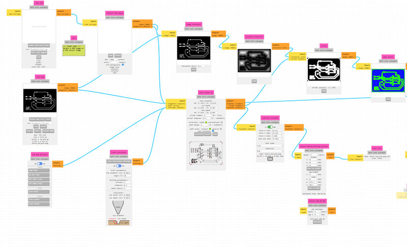
MODS CE is an online tool used to generate toolpaths for CNC machines from PCB designs. It allows you to import high-resolution images of your PCB layers, such as the copper layer and board outline, and then creates precise instructions that a CNC machine can follow to mill the board. MODS CE supports adjusting settings like cutting depth, tool size, and feed rates, making it easier to produce accurate PCBs from digital designs.Open Mods CE in your browser by visiting the link mods.programs.org.
- Click on Programs, and from the list that appears, select Roland SRM-20 PCB > Mill 2D PCB. This loads a workflow specifically configured for milling PCBs with the SRM-20 machine.
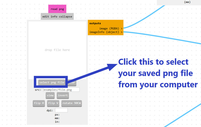
- Once the program opens, you'll see several connected modules on the screen. Click Select PNG (or SVG if your file is in that format) to upload your board image. Make sure the file is properly exported from your PCB design software, as the resolution and quality directly impact the accuracy of the toolpaths.
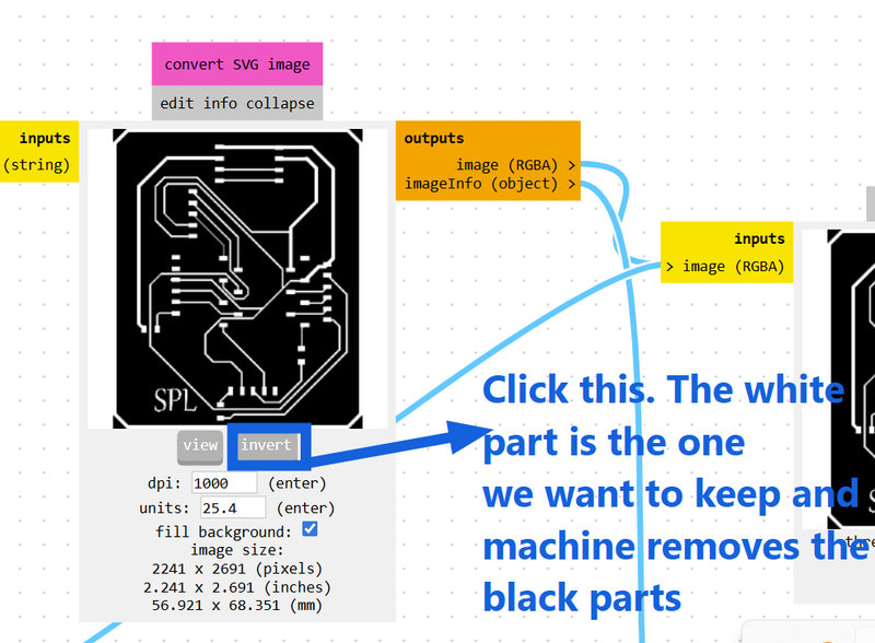
- After importing, invert the image. MODS interprets black as areas to preserve and white as areas to mill away, so inverting ensures that the copper traces are preserved while the surrounding material is removed.
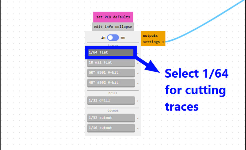
- Next, choose Mill Traces (1/64) since a 1/64 inch endmill is being used for milling the copper paths.
- Set all axes (X, Y, and Z) to 0 to define the origin point for the milling job. This step is crucial even if the axes were zeroed in VPanel, the machine relies on MODS for the reference point of the job. If the origin isn't correctly set here, the spindle may start milling in the wrong location, potentially cutting in mid air instead of on the board. Always doublecheck that all axes in MODS are properly zeroed before proceeding, as the coordinates in MODS must match the physical position of the machine to ensure precise milling.
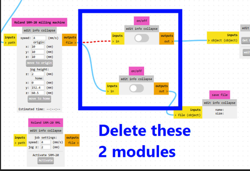
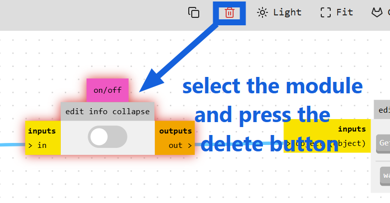
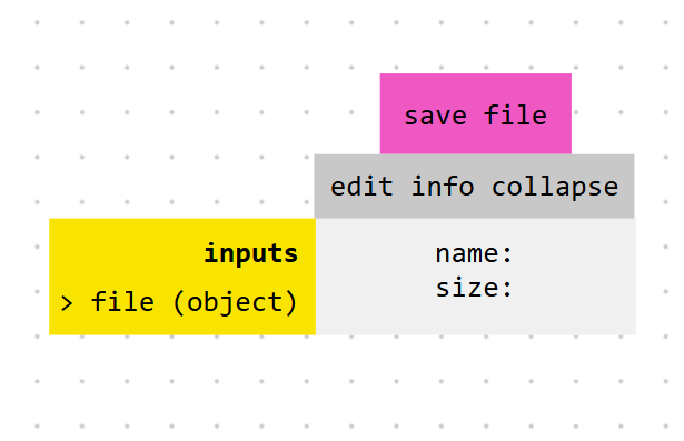
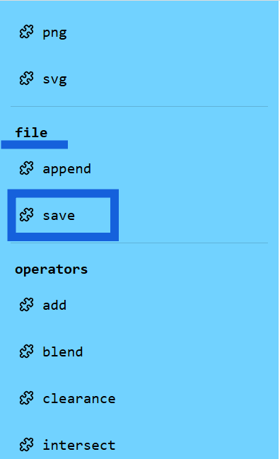
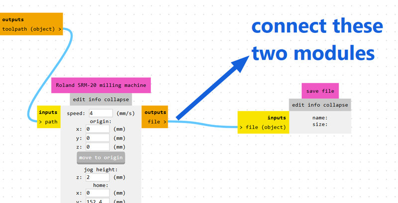
- You may see two unnecessary toggle modules on the canvas. Remove them by selecting each and clicking Delete from the top panel. Then, go to Modules → Add Module → Files → Save and connect this new module to the Roland SRM-20 output node. This ensures that when you click Calculate, the RML file is properly generated and saved to your computer.
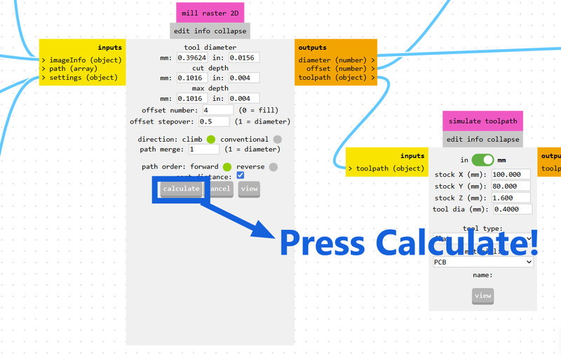
- Click Calculate to MODS generate the toolpaths and export your RML file. Then the file is ready to be sent to the SRM-20 for milling.
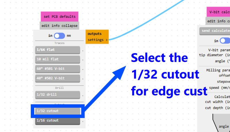
- For Edge Cuts, the workflow is the same, except you should select Mill Outline (1/32) in the tool selection step. A larger 1/32 inch endmill is used here because cutting the full board outline requires a stronger tool compared to the 1/64 inch endmill used for traces.
 - Copy - Copy - Copy_result.jpg)
This workplace should appear:
This is the toolpath of my board:
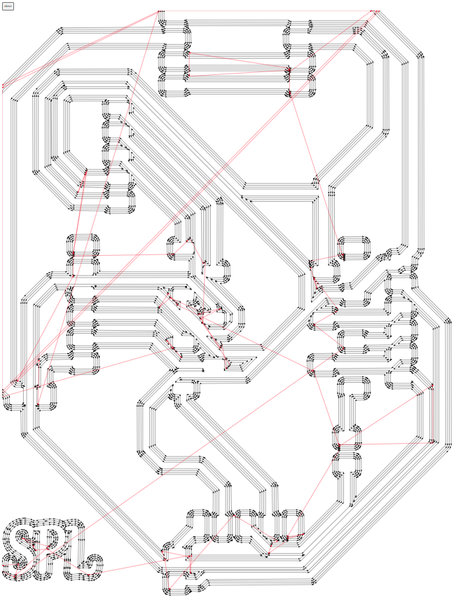
We can also simulate the PCB milling process using MODS CE. The following image shows the toolpath generated for my board.:
.jpg)
Milling Files
Prepare the Milling Bed
- Tape a sacrificial board securely onto the milling bed.
- Use double-sided tape to firmly attach the material you want to mill onto the sacrificial board.
- Ensure the material is properly secured to prevent movement during milling.
Set Up the Sacrificial Board
- Make sure the sacrificial board is flat and aligned correctly.
- A well aligned base ensures even and accurate cuts.
- This prevents uneven surfaces or errors in the final PCB.
Select and Install the Bit
- Choose the correct bit size for your milling operation.
- Secure the bit in the spindle using an Allen wrench.
- For milling traces, use a 1/64-inch bit.
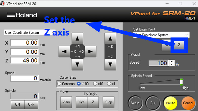
Set Up the Machine in VPanel
- Open VPanel on the computer connected to the SRM-20.
- Ensure the machine is powered on and connected through USB.
- Place the copper board on the sacrificial board and secure it with double-sided tape.
- Use VPanel controls to manually move the spindle to the desired X and Y starting position.
- Click Set X Y to zero the X and Y axes.
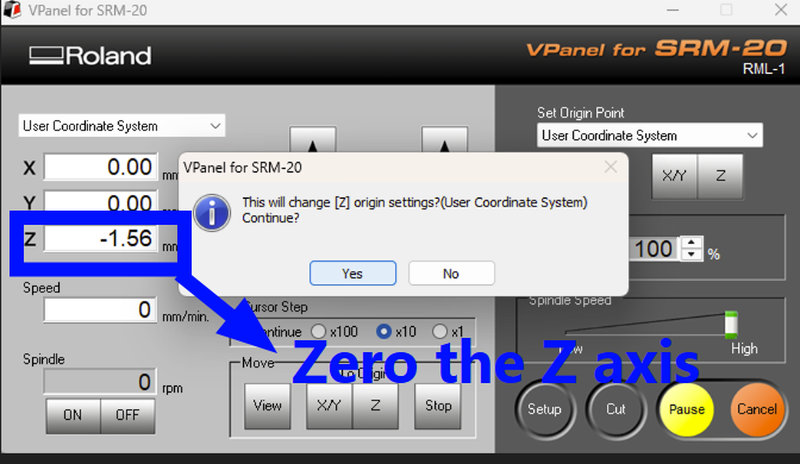
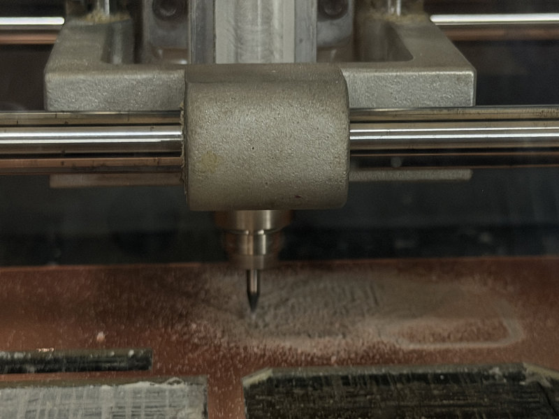
- Carefully lower the spindle along the Z axis until the endmill just touches the copper surface.
- Click Set Z to zero the Z axis.
- Verify that all three axes are zeroed,this sets the origin for the milling process.
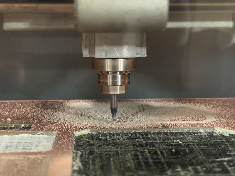
Start the Milling Process
- Ensure your RML file has been calculated and saved from MODS.
- In VPanel, click Cut and select the RML file for the traces (F.Cu layer).
- Click Output to send the file to the machine.
- Allow the SRM-20 to complete milling without touching or moving the machine.
- After traces are done, repeat the process with the Edge Cuts RML file to cut out the board outline.
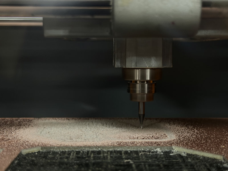
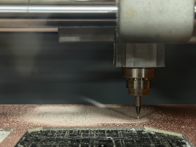
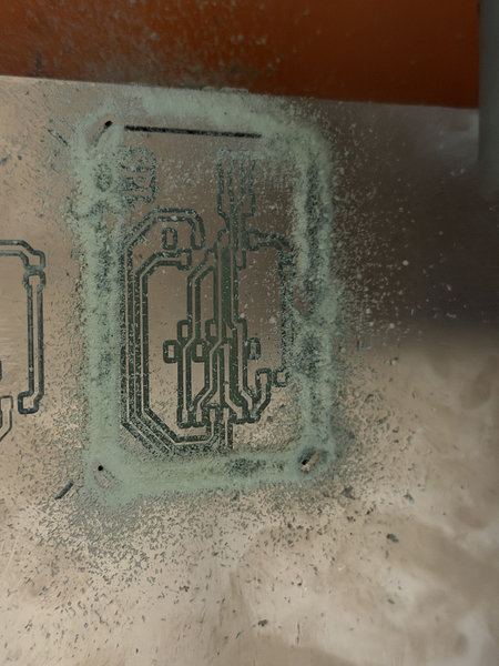
The results:
After finishing both milling steps, gently take the PCB off the sacrificial board and remove any leftover copper dust.
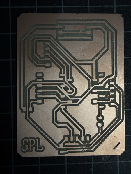
Oops! I just discovered a short circuit on my PCB that I hadn’t noticed earlier 🤦♀️
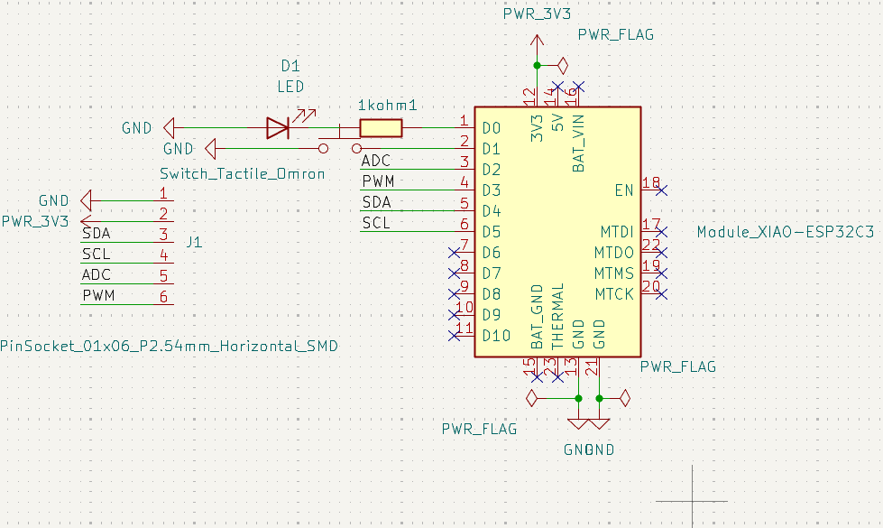
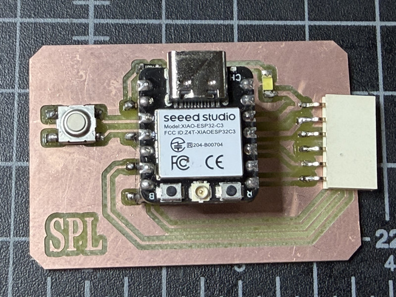
I decided to create another PCB, keeping it simpler this time, while I work on finalizing my main project board later. I designed a basic Xiao ESP32 C3 blink circuit with a button and included connector pin sockets to allow additional components for testing.
This is the schematic of the PCB designed in KiCad. I used the Xiao ESP32-C3 module and assigned it a generic socket footprint, as I did not plan to solder it directly onto the board. I also used an Omron tactile switch.
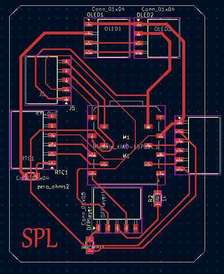
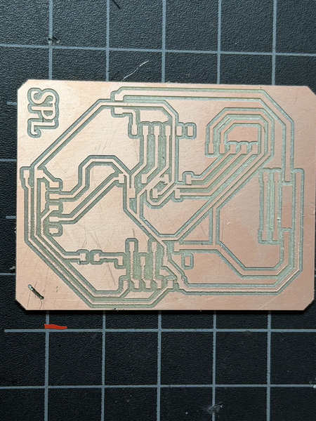
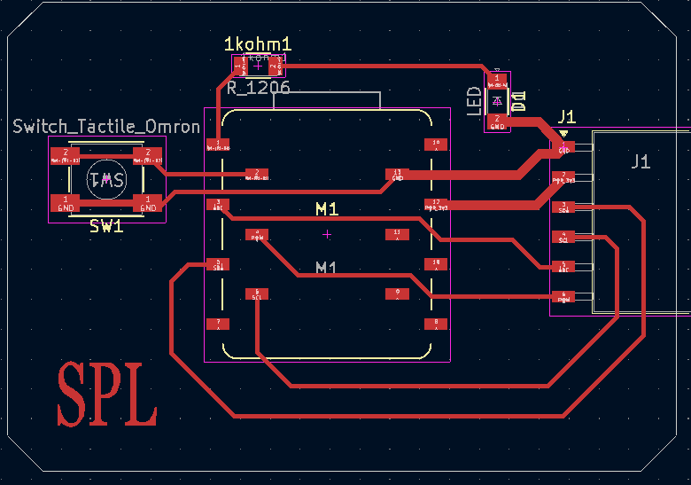
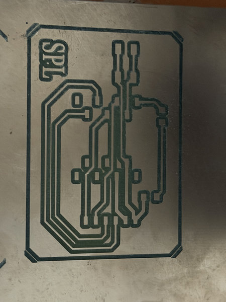
This is the PCB of the blink board, I made in Kicad. Routing was a million times easier than the pcb of my final project baord 😃
I then repeated the entire process, from editing the files in Inkscape to generating the RML file, and reset all the origin points again in VPanel.
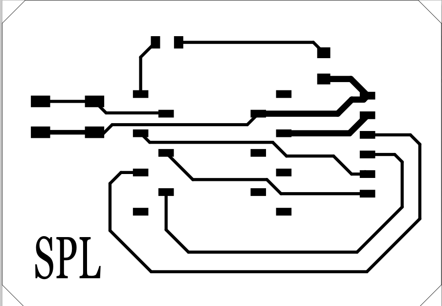
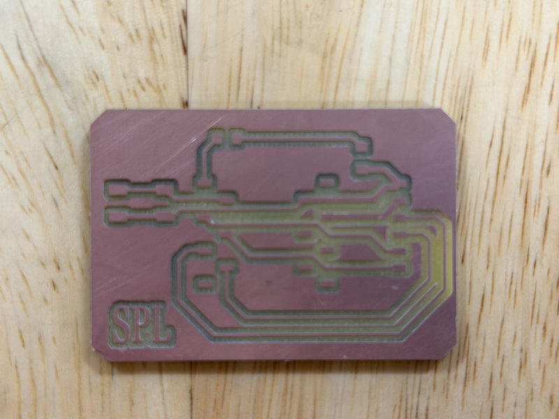
This was the toolpath of the new board and this time, no short circuits!
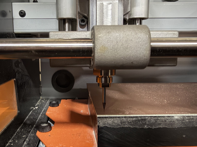
Setting the Z axis again:
Milling process:
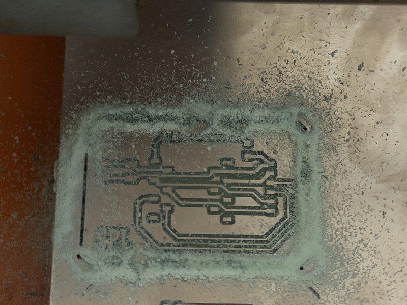
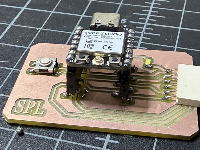
These are the results:
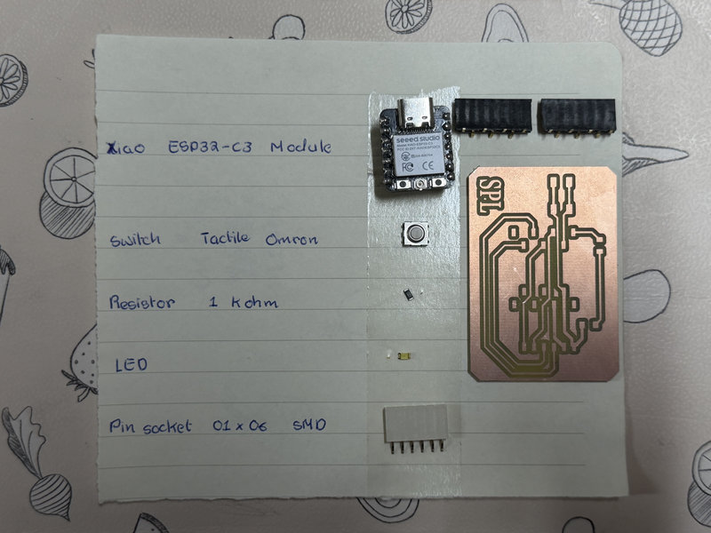
Now, to actually build the board, these are the components I will need:
Soldering the Components
Step 1: Prepare the PCB
Clean the PCB board and ensure it is free from dust or debris. Place it securely on a heat-resistant surface.
Step 2: Heat the Soldering Iron
Let the soldering iron heat up to the appropriate temperature, roughly between 300°C – 343°C.
Step 3: Tin the Tip
Before soldering, melt a small amount of solder onto the iron tip. This is called tinning and it helps with heat transfer and prevents oxidation.
Step 4: Solder the Components
Place the component on its respective pad on the PCB. Heat the solder pad and component lead simultaneously with the soldering iron, then apply solder to form a clean joint. Start with the smallest components first (resistor, LED) and finish with the XIAO ESP32-C3 last.
Step 5: Inspect the Joints
A good solder joint should look shiny and smooth with a small cone shape. If the joint looks dull or grainy, reheat it as it may be a cold joint. If solder is bridging two pads together, use solder wick to remove the excess.
Step 6: Clean the Tip
Keep the soldering iron tip clean and free of oxidation throughout the process by wiping it on a wet sponge or brass wool ball regularly.
Test the Connections
After soldering all the components, you need to make sure everything is connected properly before powering up your board.
First, make sure your PCB is not connected to any power source. Set your multimeter to continuity mode,this is usually the setting with a small speaker or sound wave symbol. In this mode, the multimeter will beep if it detects a good connection between two points.

Take the two probes of the multimeter and place one on each point you want to test,for example, one probe on a component pad and the other on the trace it should be connected to. If the multimeter beeps, the connection is good. If it stays silent, there is a break or bad solder joint somewhere that needs to be fixed.
This test helps you catch any problems like broken traces, missing solder joints, or accidental short circuits between pads before you power up the board, saving you from damaging your components.
It took me some time to solder the components, mainly because I was a beginner. Practicing on plain boards felt easier than soldering directly onto the actual PCB. My hands were shaking a lot, and some of the pads ended up with uneven solder joints, but overall, it was a really fun.
This is my soldering video:
The results:
Programming the board:
Uploading Code in Arduino IDE
Step 1: Install the ESP32 Library
- Open Arduino IDE and go to File → Preferences
- In the "Additional Board Manager URLs" field, paste this link:
https://raw.githubusercontent.com/espressif/arduino-esp32/gh-pages/package_esp32_index.json - Click OK to save
Step 2: Download the ESP32 Package
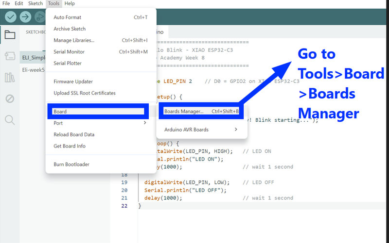
- Go to Tools>Board>Board Manager
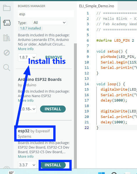
- In the search bar, type esp32
- Find esp32 by Espressif Systems and click Install
- Wait for it to finish downloading. This took me several minutes
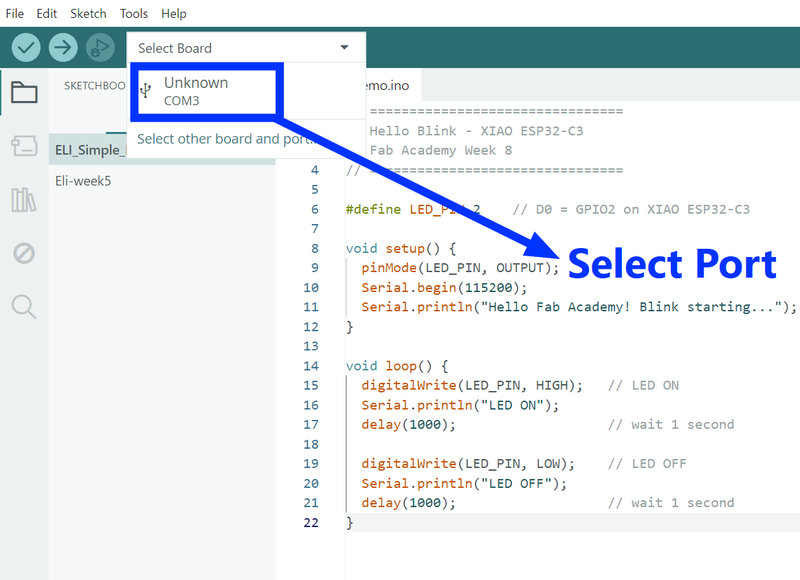
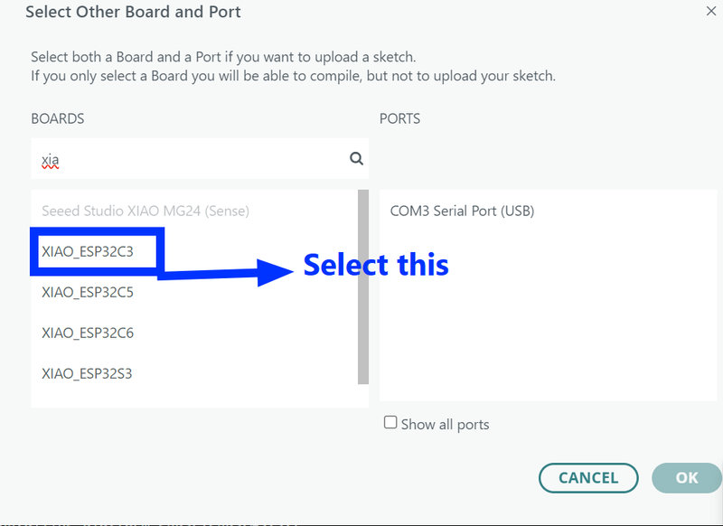
Step 3: Connect Your Board
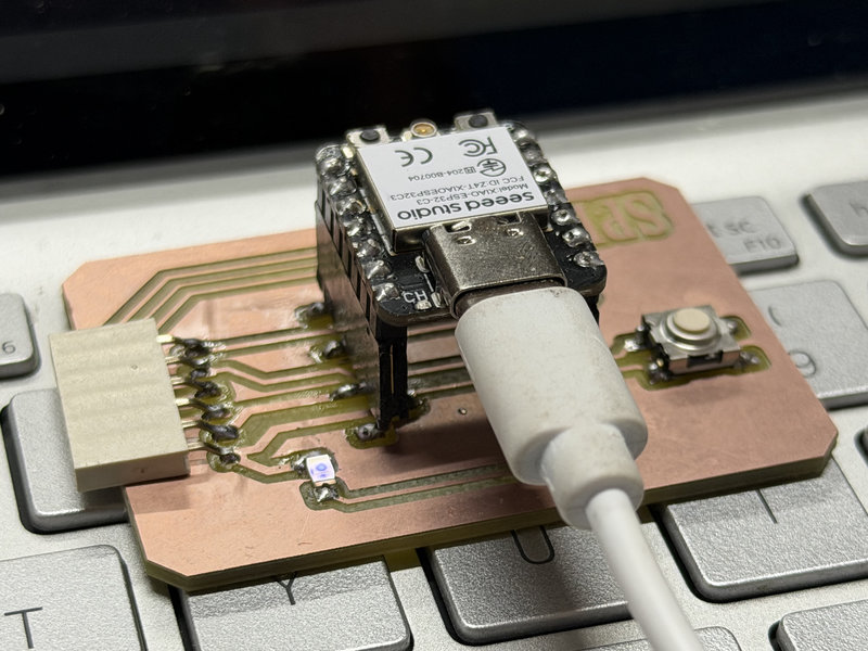
- Plug your XIAO ESP32 C3 into your computer via USB C.
- Go to Tools Port or Select Board/strong>
- Select the COM port that appears for your board and search up Xiao Esp32 C3 in the search bar. Then select the board.
Step 4: Enter Boot Mode
- Hold down the BOOT (B) button on the XIAO
- While holding it, press and release the RESET (R) button
- Then release the BOOT button
- The board is now ready to receive the code
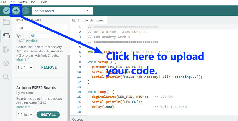
Step 5: Upload the Code
- Write or paste your code in the Arduino IDE editor
I used Claude AI to help me generate a simple blink code for my board.

This was the simple code it generated:
#define LED_PIN 2    // D0 = GPIO2 on XIAO ESP32-C3

void setup() {
  pinMode(LED_PIN, OUTPUT);
  Serial.begin(115200);
  Serial.println("Hello Fab Academy! Blink starting...");
}

void loop() {
  digitalWrite(LED_PIN, HIGH);   // LED ON
  Serial.println("LED ON");
  delay(1000);                   // wait 1 second

  digitalWrite(LED_PIN, LOW);    // LED OFF
  Serial.println("LED OFF");
  delay(1000);                   // wait 1 second
}
The LED turns on and off repeatedly every second, creating a blinking pattern.
Reflection:
The best part of this week for me was soldering the components. It was much more harder than I expected, especially since practicing on plain PCB boards felt easier than working on the actual board. My hands were really shaky, and I honestly felt like a surgeon while soldering 😆. I made several mistakes throughout the week,from designing the PCB in KiCad to milling it and soldering the components,but I’m glad I had the chance to learn from them and do better next time.