Week 6 : Electronics design
Group Assignment
- Use the test equipment in your lab to observe the operation of an embedded microcontroller
Individual assignment:
- simulate a circuit
- use an EDA tool to design an embedded microcontroller system using parts from the inventory, and check its design rules for fabrication
- extra credit: try another design workflow
- extra credit: design a case
Learning Outcomes
- Understand how to choose and use suitable software for circuit board design.
- Demonstrate the workflow involved in designing and preparing a circuit board for production.
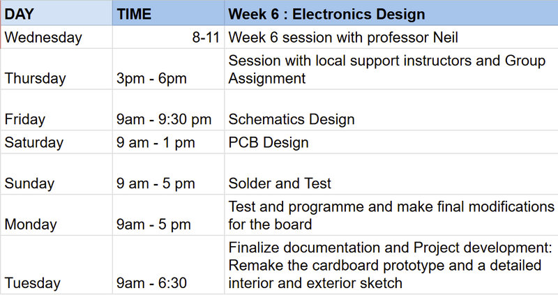
This is the schedule I made for this week to help me manage my time efficiently:
Group Assignment:
This week, our group worked with two key pieces of test equipment in our lab: an oscilloscope and a multimeter. You can access our group assignment here.
.jpg)
Our local instructors, Dawa and Yangtshel, walked us through the basic features of both tools and helped us get hands on with them.
For the oscilloscope, we used the GDS-1202B by GW Instek, a digital storage oscilloscope. To test it, we hooked it up to a sound sensor circuit and watched how the waveform changed in real time based on sound. Louder sounds made taller waves, softer sounds made shorter ones, and high vs. low pitch affected how close together the waves appeared. This helped us observe both digital and analog signals in action.
.jpg)
.jpg)
With the multimeter, we practiced measuring resistance, testing continuity, and measuring voltage. We learned how each measurement requires a different connection setup,for example, resistance is measured with the circuit off, while current requires breaking the circuit and measuring in series.
.jpg)
Overall, the main takeaway was understanding how these tools let you see inside a circuit. The oscilloscope shows you how a signal behaves over time, while the multimeter gives you precise numerical readings of electrical properties. They're both important for debugging and understanding any electronics project.
Individual assignment:
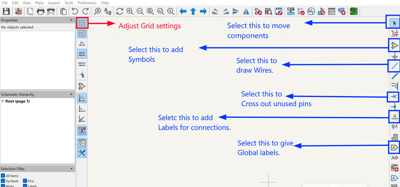
Kicad
The EDA software I'll be using for my board is Kicad
KiCad Tutorial: Make Your First Printed Circuit BoardKiCad is a free, open-source, and user-friendly electronic design automation (EDA) software suite that streamlines PCB design from schematic to layout. It is considered "simple" due to its intuitive, integrated interface, large community support, and lack of paid "premium" limitations. It is perfect for beginners and professionals alike.
Key Components
KiCad consists of a suite of integrated tools, each dedicated to a specific stage of the PCB design process:
- Schematic Editor (Eeschema) – Used for creating electrical schematics. It allows the designer to place components and define the logical connections between them.
- PCB Layout Editor (Pcbnew) – Translates the schematic into a physical board layout. This tool is used for component placement and routing of copper traces.
- Footprint Editor – Enables the creation and modification of footprints, which define the physical copper patterns and land dimensions for mounting components on the board.
- Symbol Editor – Used to create or customize schematic symbols, which represent components logically in the circuit diagram.
- 3D Viewer – Generates a three-dimensional visualization of the PCB. This is useful for verifying mechanical fit and producing realistic renderings of the assembled board.
Schematics
A schematic in KiCad is a digital, 2D diagram that acts as the blueprint for an electronic circuit, showing how components like resistors and ICs connect using symbols and wires. It is the starting point for PCB design, allowing you to define electrical connections, check for errors, and generate a netlist for the layout process
- Symbols are the logical representations of electronic components used within a schematic.
- A footprint defines the physical arrangement of pads on a PCB.
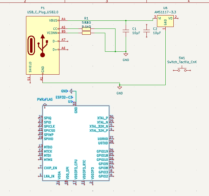
I began creating my schematic by referring to this image as a guide. Since the board is intended for my final project, the main components I needed to design were the pin headers for connecting the project parts, like the image below.

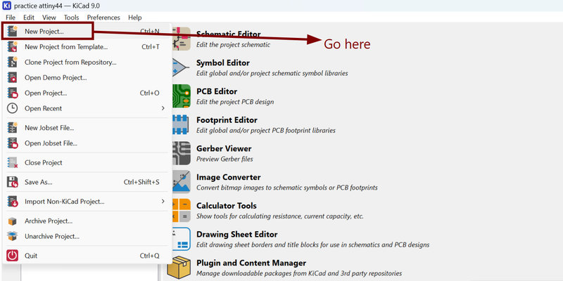
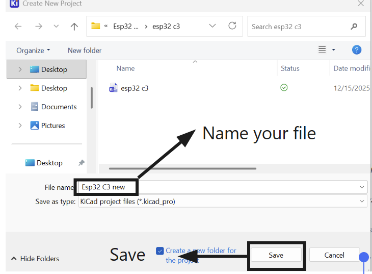
Starting a New project in KiCad:
- Go to 'File' and select 'New Project' from the dropdown.
- Then name your file.
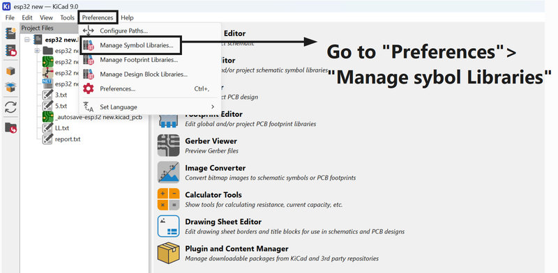
Adding libraries:
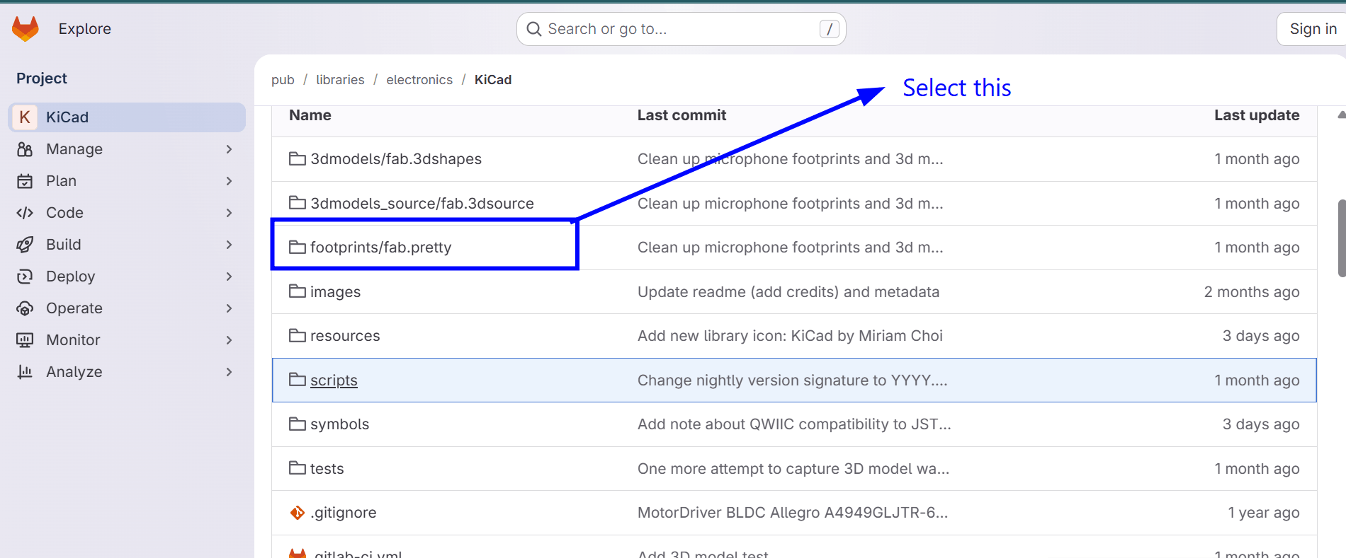
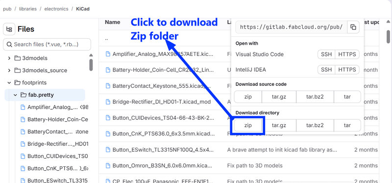
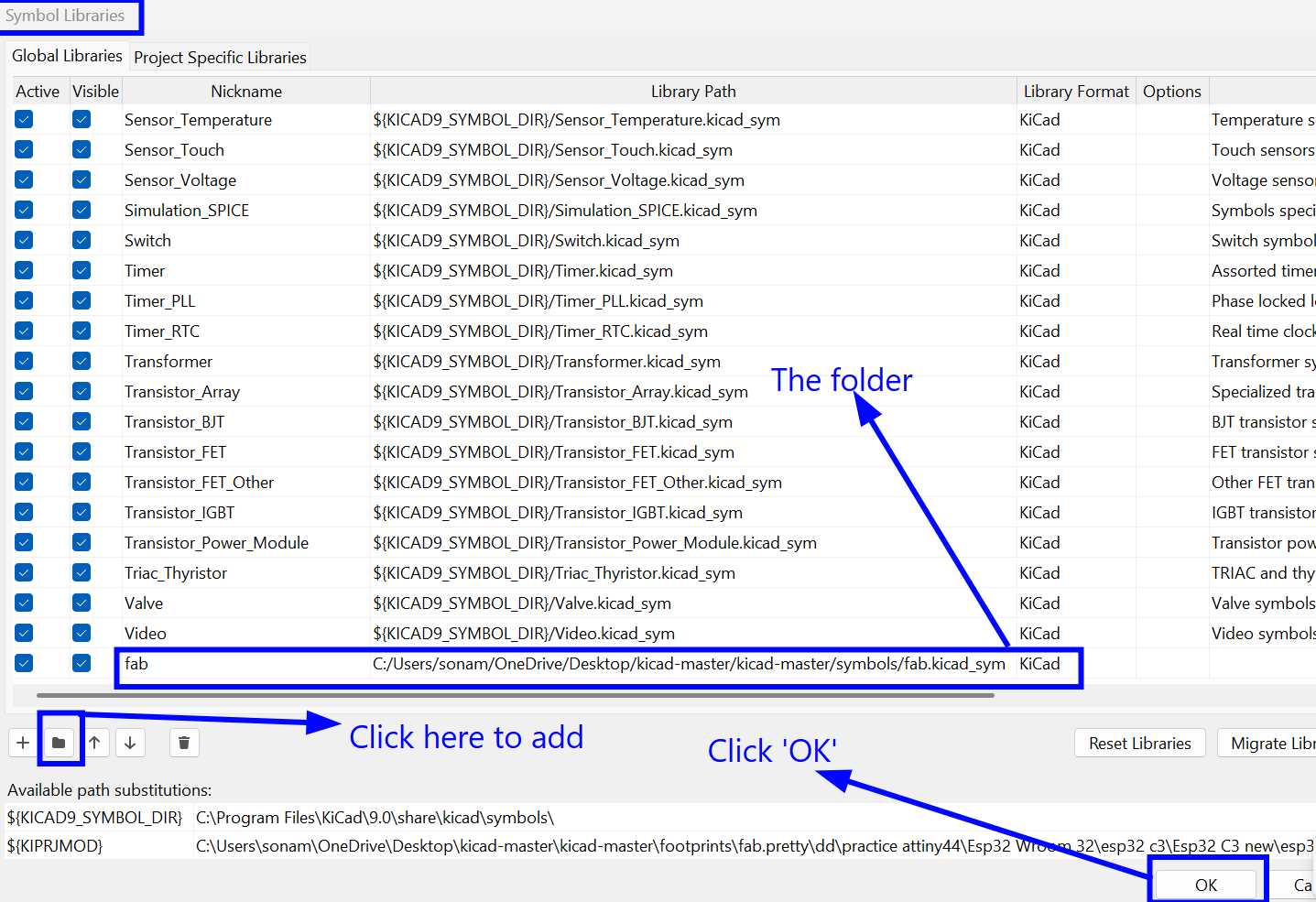
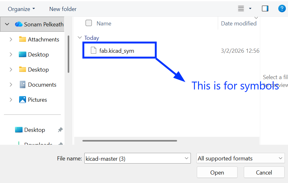
Here is the label for the workplace.
Adding Symbols:
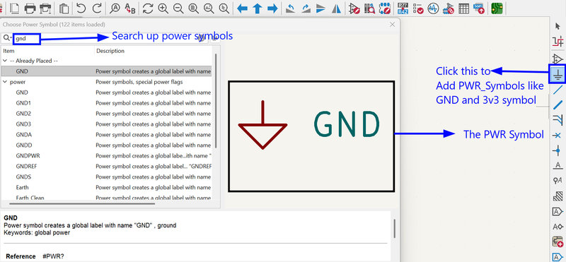
Adding Power Symbols:
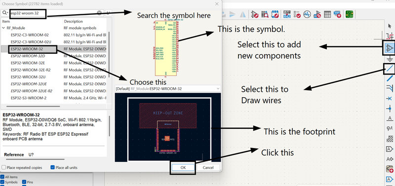
I placed all the required components onto the workspace. The components I used included:
- Conn_01x06
- Conn_01x05
- Conn_01x04 (×2)
- Conn_01x02
- PinSocket_01x05_P2.54mm_Vertical_SMD
- PinSocket_01x02_P2.54mm_Vertical_SMD
- 10kΩ resistor
- 1kΩ resistor
- XIAO ESP32-C3
After placing all the required symbols in the schematic and completing the electrical connections, the next step was to link each component to its physical representation on the PCB.
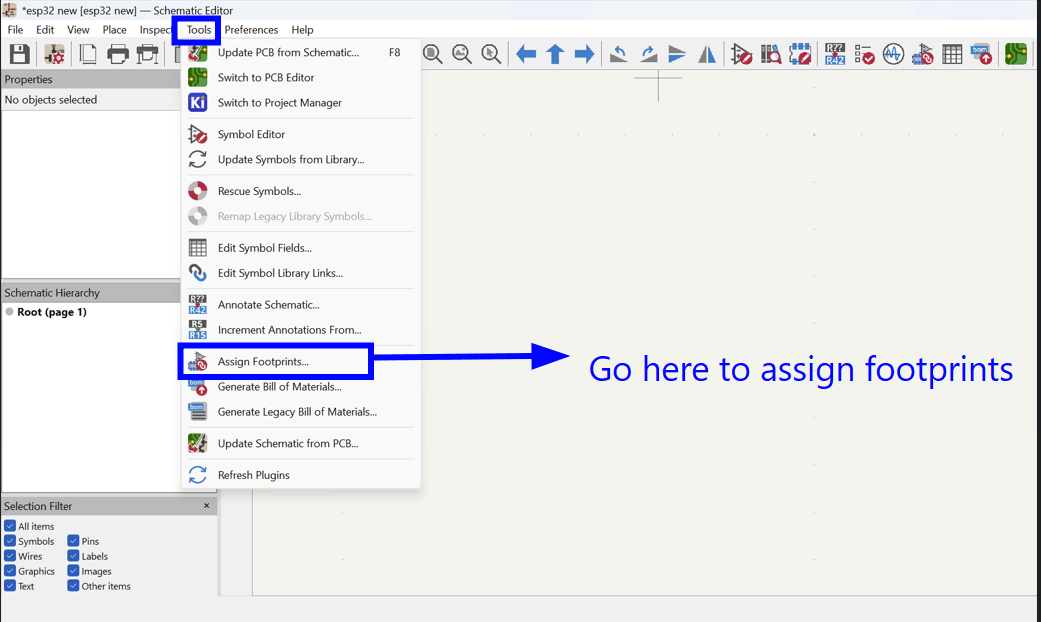
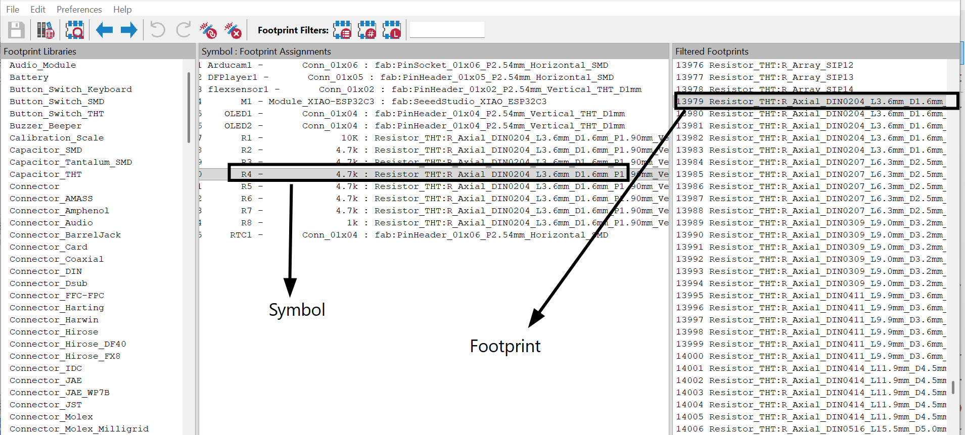
Assigning Footprints:
In KiCad, footprints represent the actual physical layout of a component on the board. They define where the pads are placed, their size and spacing, and how the component will be soldered onto the PCB. In simple terms, while the schematic shows how components connect electrically, the footprint shows how they exist physically on the board.
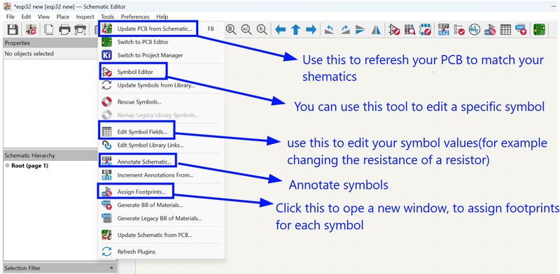
To assign footprints, I opened the Tools menu and selected "Assign Footprints" to match each schematic symbol with the correct PCB layout.
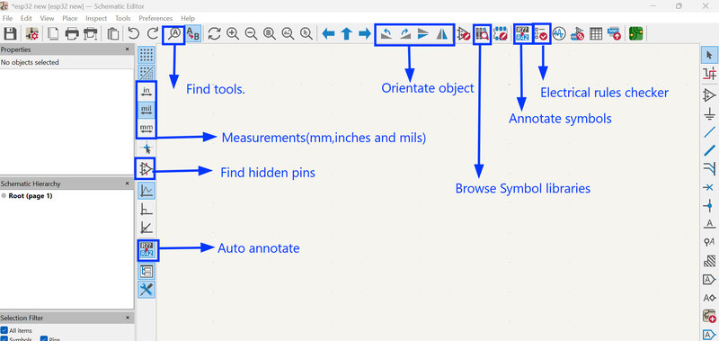
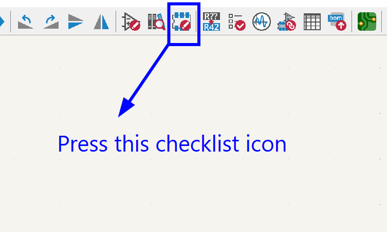
Electrical Rules Checker:
The Electrical Rules Checker (ERC) in KiCad is a tool that automatically scans your schematic for common electrical mistakes or rule violations. It works like a spell check for circuits, identifying issues such as unconnected pins, duplicate net names, incorrect power connections, and other potential errors. Running ERC ensures your design follows proper electrical standards and helps catch problems early, making the transition to PCB layout smoother and reducing the chance of costly mistakes.
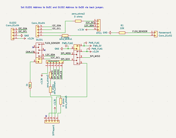
Creating a schematic for my final project took quite some time, especially as a complete beginner in KiCad. I made numerous mistakes and had to run the ERC several times to fix all the errors.One mistake I made was using the XIAO ESP32 C3 bare chip. I was already halfway through designing the necessary voltage regulators and the EN switch when I found out that it would have been fine to use the module instead for my project .The mistake was because of my own carelessness
One silly mistake I made was using THT connector pin headers instead of SMD ones, which meant I had to reassign footprints halfway through designing the PCB.
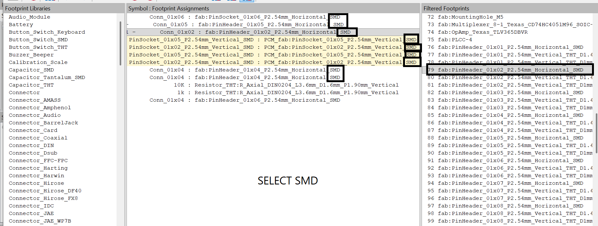
Another mistake I made was choosing the wrong footprint for the ESP32-C3 module. Instead of using the Xiao generic socket SMD footprint, I selected the standard connector pin headers that I had used for the rest of my components. Initially, I used the Xiao ESP32 module without assigning the generic socket footprint, leaving the chip footprint by default, which wasn’t correct since I wasn’t soldering the chip directly to my board.
Later, I made another mistake by selecting the regular connector pin header symbol for the Xiao module, just like I did for the other components.I actually got pretty far with my board before I even realized I had chosen the wrong footprint!
.jpg)
.jpg)
How I Made the Connections
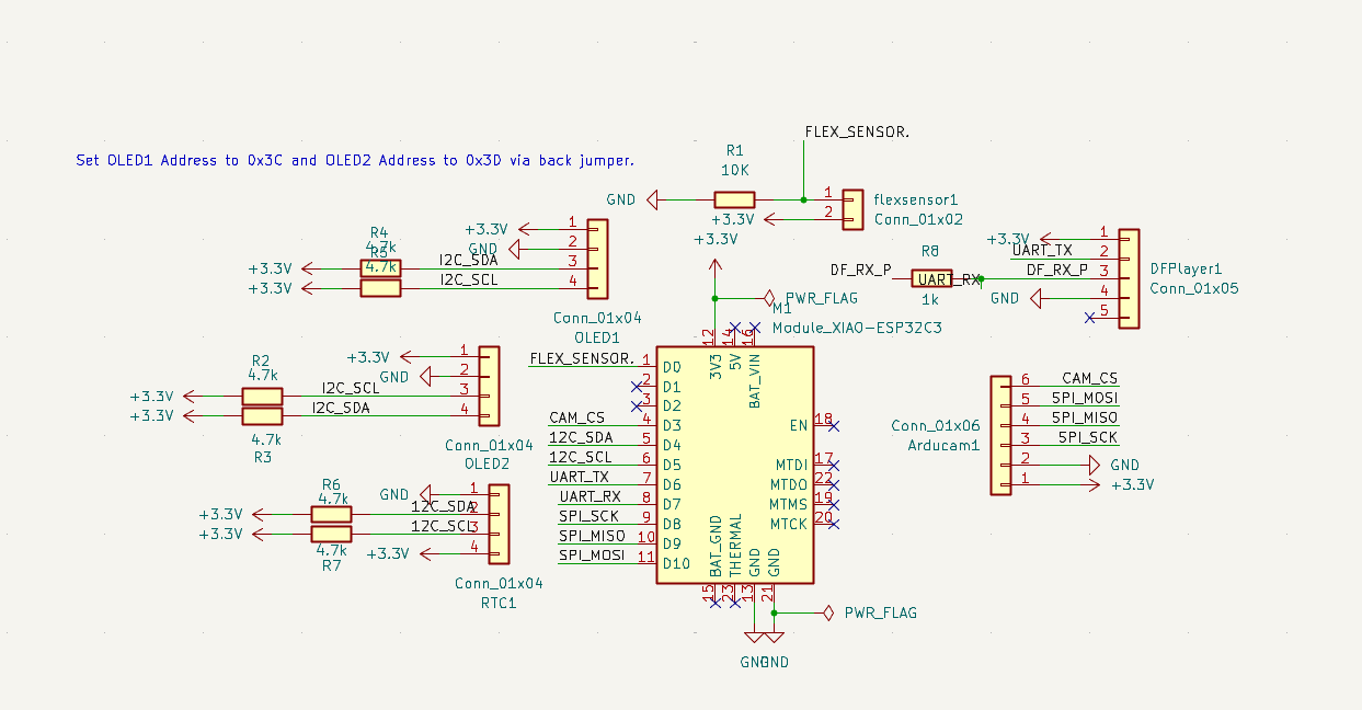
Since I was designing the board for my final project, I had to add pin headers for the specific components I planned to use. I used Conn_01x04, Conn_01x05, and Conn_01x02 symbols depending on how many ESP32-C3 pins each component required.
After placing the appropriate connectors, I labeled them to the corresponding GPIO pins of the ESP32-C3. I also added a resistor for the flex sensor.
The RX and TX connections took quite a bit of time to get right. The RX kept connecting to RX and TX to TX instead of RX to TX. I initially tried using labels to link them, but when I moved to the PCB layout, the RX and TX were not connecting correctly. In the end, I directly connected them using wires in the schematic, and that solved the issue.
.jpg)
After what felt like an eternity of tweaking, and fixing mistakes, I finally finished designing the schematics for my final project board.🥳
.jpg)
I used labels to make all the connections look cleaner and more organized. To add a net label, select the "A" icon or press Ctrl + L.
I learned about two types of labels:
- Global Labels – These are used to create connections across different schematic sheets.
- Net Labels – These are used to name nets or connections within the same sheet. To add a global label, press the icon that looks like a tag with the letter 'A' in it.
Annotate
In KiCad, annotation is the process of giving each component in your schematic a unique identifier or reference designator. These identifiers make it easy to tell components apart and are crucial for keeping your circuit organized and correctly assembled. Annotation ensures that every component has a distinct name or number, which helps prevent mistakes during both the design and assembly of the physical PCB.
To annotate your schematic, go to "Tools" in the top menu and select "Annotate Schematic."
.jpg)
Switching to PCB Editor
From the 'Tools' dropdown, select Update PCB from schematics.
.jpg)
PCB Workplace
.jpg)
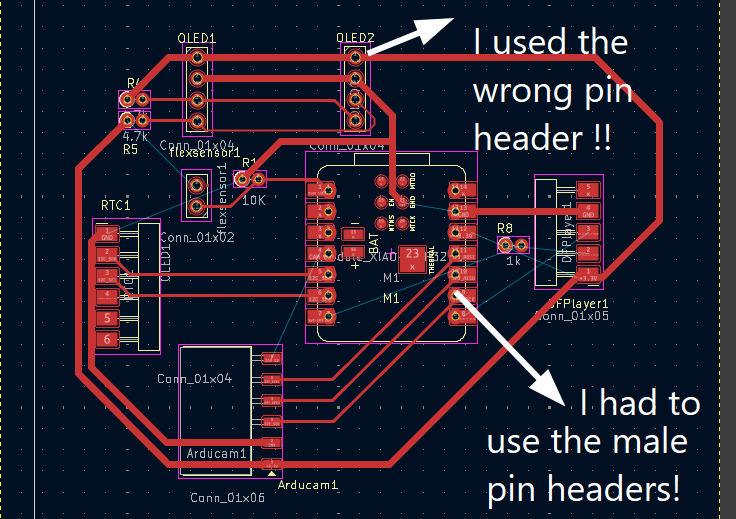
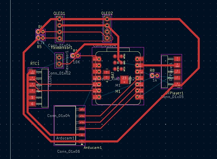
These were all the components I had to route 😣
.png)
First, I arranged all my components to make routing easier. I made sure to avoid positions where the blue guideline lines overlapped too much. I also adjusted the orientation of some components to achieve a cleaner layout with fewer overlapping lines.
.jpg)
Then I started routing, and wow, it took a really long time 😵💫 especially when having to tweak your schematics time and again because of the footprints confusion. If you’re someone who loves puzzles and mazes, you’d probably love this. Me....... not so much 🥲
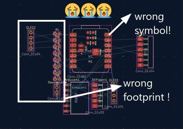
But oops! I forgot that I didn’t need to solder the ESP directly onto my board, so I had to switch to vertical female pin headers. On top of that, I had chosen the wrong footprints for most of the other pin headers,they were supposed to be surface-mounted, not through hole.
.jpg)
Routing is definitely not my thing, but I guess practicing is the only way to make progress! ^_~
.jpg)
.jpg)
.jpg)
.jpg)
.jpg)
God knows how many times I got stuck😵 There was always one pin that just refused to work with me. (┬┬﹏┬┬)
.jpg)
To fix the issue, I added zero ohm resistors, which solved the stubborn connections.
.jpg)
.jpg)
After what felt like a whole ice age passing by, I finally finished my PCB!🎉
.jpg)
Adding the Edgecut Border Line
I added the border line, which defines the shape of my board and will be used by the milling machine to cut it out.
.jpg)
.jpg)
Design Rules Checker
Just like I ran the ERC for my schematic, I also ran the Design Rules Checker for my PCB to make sure there were no design errors and to help me improve the board
_result.jpg)
3D Viewer
Then I clicked on the 3D viewer to check how my board looked like in 3D. The KiCad 3D Viewer is a tool for visualizing your circuit board in 3D to check for component clashes, verify mechanical fit in enclosures, and inspect the final look of the board. It provides a realistic, rotatable model that updates automatically as you make changes in the layout.
.jpg)
.jpg)
.jpg)
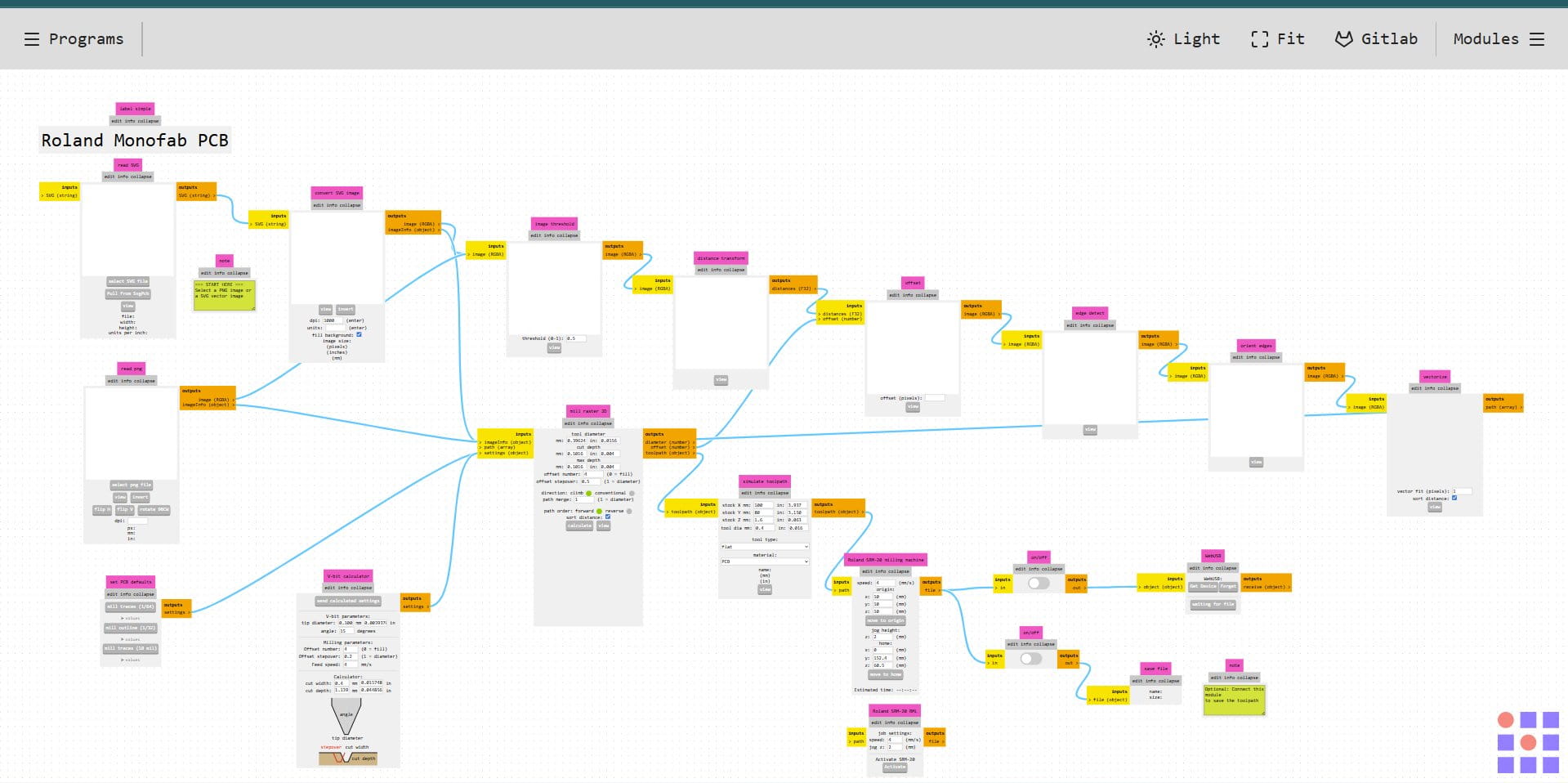
Mods CE
Mods CE is a browser based CAM (Computer-Aided Manufacturing) tool that converts your PCB design files into machine-readable instructions. You load in your exported board image, set parameters like cut depth and tool size, and it generates the toolpaths that tell the milling machine exactly where and how to cut your copper traces and board outline.An RML file is the output file generated by Mods CE, it contains the movement instructions (toolpaths) that tell the milling machine exactly where to move and cut.
I referred to Azhim Tsheltrim’s Week 6 assignment page, which provided me with a lot of helpful guidance. These are the steps I followed to generate the RML file, the process is actually really easy, and it took me like 15 minutes.:/p>
First export your board layer as SVG in Kicad:
.jpg)
.jpg)
Then search up Mods CE in your browser.And then, I did the following procedures:
.jpg)
This workplace should appear:
.jpg)
Steps to Generate the RML File in Mods CE
- Insert your design file (SVG or PNG) into Mods CE.
- Invert the image.This is important because Mods CE reads black areas as parts to keep and white areas as parts to remove. Inverting ensures the traces are preserved while the surrounding copper is milled away.
- Select Mill traces (1/64 inch) since a 1/64 inch endmill is used for cutting the copper layer. This bit has a fine 0.4 mm tip, allowing precise isolation of PCB traces without damage.
- For edge cuts, repeat the same process but select Mill outline (1/32 inch) in Step 3 instead. The 1/32 inch bit (0.8 mm) is larger and stronger, making it suitable for cutting the outer board shape.
- Set all axes (X, Y, and Z) to 0 to define the machine's origin point.
- Remove the two unnecessary on/off modules by clicking on the module and when the module highlights, select delete from the top toolbar.
- Go to Files Save and connect the file to the Outputs folder.
- Click Calculate and your RML file will be generated and is ready to be sent to the milling machine. A preview will be shown below.
.jpg)
.jpg)
.jpg)
.jpg)
.jpg)
.jpg)
This is the preview of my SVG for the F.Cu layer of my board:
.jpg)
.jpg)
I repeated the whole process again to generate an RML file for my board edge cuts layer:
.jpg)
Reflection:
If I had to describe this week in emojis, it would be: 😵💫😵🪦⚰️.Even though this week was relatively harder than the previous ones, and knowing the coming weeks will be even tougher, I learned so many things that I couldn't have without always having everything easy.
Routing was annoying, yes, but also really fun like some game. And, I got to work on my final project board, which is a huge step forward. So, yay to that! 🥂