Week 6
Check List
This week's project requirements:- Use the test equipment in your lab to observe the operation of a microcontroller circuit board
- As a minimum, you should demonstrate the use of a logic analyzer
- Document your work on the group work page
- Reflect on what you learned on your individual page
Individual Assignment:
- Simulate a circuit
- Use an EDA tool to design a development board that uses parts from the inventory
- It should interact and communicate with an embedded microcontroller
- Check its design rules for fabrication
- Document the process
Images/Files:
- Include your original design files
- Properly compress or use a zip folder if needed
- Include hero shots of your results
Extra credit:
- Try another design workflow
- Design a case
Group Assignment:
Resources and Helpful Links
- KiCAD
- Seeed Studio Blog
- Seeed Studio Wiki
- Chat GPT
- WokWi
- Helpful People:
- Thomas Dubick, Dr Taylor, My Father, My Group Partners Camille, Kim, and Dorian
- Thomas Dubick, Dr Taylor, My Father, My Group Partners Camille, Kim, and Dorian
Learning Outcomes
- Select and use software for circuit board design
- Demonstrate workflows used in circuit board design
Group Work
My Contribution to the Group Work
My group tested out two different quality of multimeters, an oscilloscope, and a logic analyzer. As a group, we really worked together to learn and use each of the tools. We each used our background skills and knowledge and shared what we could. For the tools we did not know, like the analyzer, we worked together to learn how to use it. We called for some additional help and as we started to understand what we were doing we shared with each other so we all felt confident with the tools!
I am very grateful for having a group for this assignment, because we reallly did help each other tremendously!
-
My Contributions to this week:
- I used one of the multimeters to test that the LED's we were using were not dead. I read the forward voltage of the led to be 1.8V.
- I helped troubleshoot our breadboard setup by finding that we had a resistor in the wrong pin location.
- I helped my groupmates with additional testing using the multimeters as needed.
- I, along side Dorian, calculated the Ohms Law values for our circuit to compare to our measured values. We both did the calculations so we could compare with each other as a check system.
- I helped with setting up and using the oscilloscope since only myself and Dorian had previous experience with one.
- I brefily explained to my group mates what the purpose of an oscilloscope is and why we would use it. For example we can use it to see the shape of a signal.
- I helped Camille with setting up the Logic Analyzer and worked with my group mates to figure out how to use it.
Before this activity, I understood Ohm's law, how to use a multimeter and the basics of electrical signals. It had been some time since I used and oscilloscope, and I had never used a logic analyzer before. It was really nice to refresh my memory with the oscilliscope and the logic analyzer forced me to think differently about electrical signals and how to analyze them. I found the logic analyzer to be challenging at first, and a little intimidating, with all the wires coming out of it. Without the correct wiring with the probes, and the correct settings, triggers, and channels set up, we were not able to see anything. It was hard to tell where the problem was with so many possible variables to check.
Overall, I learned that the logic analysis is closer to debugging tool than a tool for measuring electricity. Once we got it working I learned that it is a very powerful tool for understanding the behavior of a circuit. It was really cool to see the signals in real time and view the distinction between an on and off state. It was also really interesting to see how adding something like a capacitor can drastically change the shape of the signal.
You can view our documentation on our experience with each tool on our Group page.
Installing the Library and Footprints
Getting Started
The first thing I needed to do to get this week started was to download the library and footprints package for the Xiao ESP32C6 board I was planning to simulate. I wanted to create my dice project from week 4 as a possible board I can build in the near future.
I had never installed a library or footprints into KiCAD before so I turned to chatGPT to get a starting point. You can view my conversation here and here . It is in two parts because I was on a temporary account on my work computer and I was not able to save the entire chat history like I do while on my own account, but I was able to save all parts just individually. I did save a pdf copy of the chat with my prompts, which is available to view in my week 6 file folder.
While looking for the files for step one, I tried navigating the github that was linked from chat but I found that I wasn't easily able to find the files I needed. I tried a quick google search which led me to a Reddit post which had a repsonse with some helpful links. One of the links was for a blog post by Seeed Studio which talked about using Xiao boards in pcb creation. This was a very informative article as it talked a little bit about the boards history, the design of Xiao boards, different ways to mount the boards to a pcb, and suggested some PCB design software. It did not however have the files I needed.
Through an additional Google search, I found my way back to the Seeed Studio Wiki that I reviewed in week 4. Using control-F I was able to search the Wiki Page for KiCAD and I was qucikly brought to direct file donwloads for the XIAO Series KiCAD Footprints and KiCAD SCH Symbols.
I found this to be a much easier method then trying to navigate the Seeed Studio github.
As a side note: Camille, Kim, Dorian, and myself have all shared our boards library and footprint donwload files/folders with each other in a shared Google drive. This gives us quick and easy access to the necessary files if we want to try creating designs for differnt boards. We also shared our notes about our boards and the installation processes with each other.
Installing the Libraries
After downloading the files, I was ready to install the libraries into KiCAD. The first thing I did was open KiCAD. Once in KiCAD, I opened the symbol editor by going to Preferences > Manage Symbol Libraries.
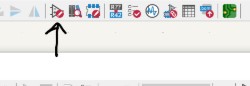
In the symbol library menu, I navigated to File > Add Library > Global > Find and Add.
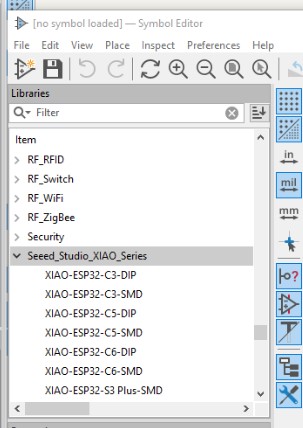
This opened up my file explorer and I navigated to the downloaded .kicad_sym file and added it to my libraries. I chose to use the global option versus the project option, so that I can use the library in future projects without having to add it again.
Next I opened the footprint library menu by going to Preferences > Manage Footprint Libraries.
In the footprint library menu, I again navigated to File > Add Library > Global > Find and Add.
This time I added the .pretty file I downloaded from the Seeed Studio Wiki. Both the footprint and symbol libraries can be found in my week 6 file folder below.
Designing my Dice Board
Creating the Schematic
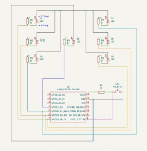
After downloading and installing the Xiao libraries I was ready to design my dice board. As stated earlier, I wanted to create a physical board for my simulated dice project from Week 4 . I started by adding and orienting 7 leds, 8 resistors, 1 button, and 1 xiao esp32C6 board.
To add the componenets to the schematic, I pressed “A” which is a keyboard shortcut for the add component tool. The add menu is also found on the right hand side of the screen and looks like an op amp symbol.
This opened up a search menu where I was able to search for each component by thier names: Xiao ESP32C6, LED, resistor, and button.
Once I added all of the components to the schematic, I needed to organize them on the screen and connect them with wires. The keyboard command for the wire tool is “W.” You can also find the tool on the right hand side of the screen, it looks like a slanted line.
I used my Wokwi simulation build to help wire the board. To make the wires, I activated the wire tool and then clicked on the pin I wanted to start from and then clicked again on the pin I wanted to connect to. After wiring everything up I needed to assign each of my components a footprint so that I could see them in the PCB editor. I opened the assign footprint menu by going to Tools > Assign Footprints and matched each component to its real world counterpart.
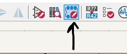
With all the components wired up and thier footprints assigned, I was ready to run the electrical rules check and see if there were any errors with my design. Unfortunatly, thier were a handful of issues.
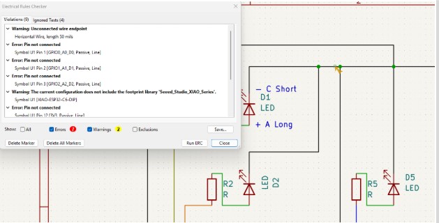
The quickest and easiest error to fix was the overlapping wires at the top on my ground.
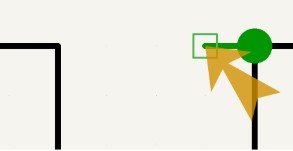
Camille actually recognized the symbol as she had just solved this issue on her schematic and she shared with me that I needed to delete the wires and find the overlapping one. I did so and rechecked and the error was gone.
The next issue was all of my crossing wires. Initially, I wired up the project the same way I did in my simulation, however I realized this wiring would not work on the board due to the wires crossing in many places. I could have used zero ohm resistors as jumpers to solve this issue, I also could have moved the resistors I was already using to better locations, but I decided to rewire the board instead.
Wiring this board without crossing wires was like the worst brain puzzle I could have done. I kept thinking about those dot puzzles/riddles that have you connect the dots without crossing the lines. This was exactly what it felt like:

Typically there's a clever solution to these kinds of puzzles. Since wiring this board felt just like the puzzle, I kept thinking like how I would solve this kind of puzzle. But the clever solution wasn't easily coming to me. I took it one line/component at a time and eventually got it all wired up. I think I over thought it too much and overcomplicated the wiring process. Thinking back, putting in the zero ohm resistors would have been quicker, but I am happy with figuring it out.
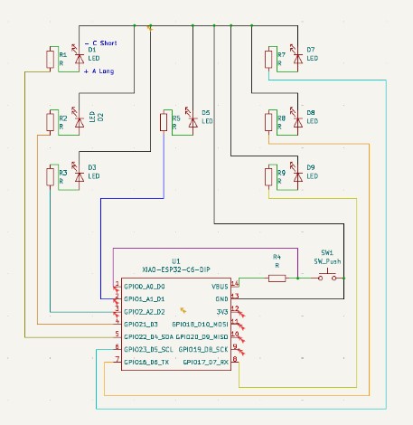
This new wiring requires me to go back to my dice program and adjust the code so that each LED has its own separate control pin. This was one of the few ways I found worked to have no crosses on the LEDs. To ensure no other crosses I also had to adjust the button pin from pin 8 to pin 1. Recoding my dice program with this new pin setup will be a problem for future me.
I ran the electrical rules checker again and most of my errors cleared except for the warning I got about the footprint library for the xiao board.
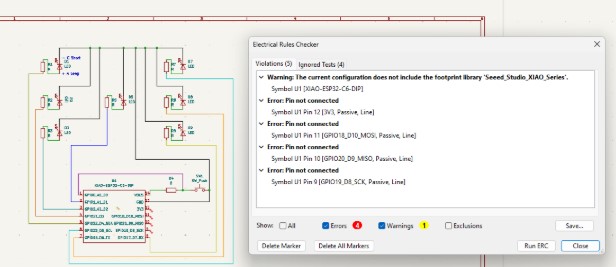
I went back to the footprint library, followed the steps again and tried installing the library again with no luck. Then I tried editing the footprint I was able to view, with no luck. Finally, with a suggestion from Camille who had a similar issue, I right-clicked on my xiao board in my schematic and chose the Edit Main Fields > Edit Footprints.
Here, I loaded the footprint libraries directly and was able to select the ESP32C6 DIP option instead of the Xiao Add-On that was the only option I had when I went into the assign footprint menu. This solved my rules check error and I was now able to see my board in the PCB editor and connect wires to it. With the add-on board I was able to add it directly and see it in the PCB editor but I wasn't able to connect anything to it.
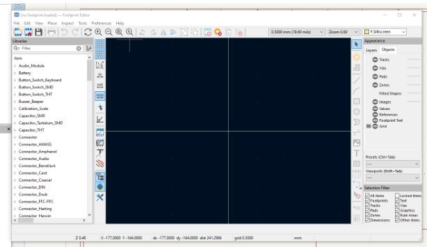
Editing the Board in the PCB Editor
Now that I cleared all of the errors in the rules check and was able to see and attach wires to my xiao in the PCB editor it was time to set up my PCB design.
I moved all my pieces around to a neat formation and begand wiring the LED's to the resistors.
I had a really annoying issue with the resistors and leds though.
I wanted to mirror them so my resistor and led pads were next to each other for cleaner wiring, but the mirror button did not work.
No matter how many times I tried it, whether clicking the button or using the keyboard command, or how I had things selected it just wouldn't work.
I was able to get what I was hoping for though using the rotate tool, but it was a bit fustrating to not have a tool work as expected.
I got everything wired up in the PCB editor and took a look at the design.
I used the following design rules while setting up my board in the PCB editor.
- Trace width = 0.25mm which is the default
- Minimum Clearance = 4.5mils which was the default
- I did not use any vias since I was able to route everything on one layer.
- I did not use any net classes, but I did make sure to connect all of my grounds to the same ground on the xiao board.
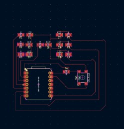
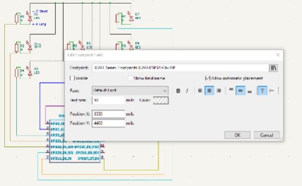
I wanted to make my board more than just a square, so I extended the leads to the dice LED's a bit further and added Roll the Dice in the middle as part of the silk screen. I may go back and try to make the board shape and silk screen look more like a 3d dice effect, but for now I was happy with the shape. Finally, I looked at my board in the 3D view.
I was happy with it, until it was pointed out that my esp32C6 was upside down and the usb connector was in the middle of my board. My board will work as it stands, but the wire will get in the way. I was heavily encouraged by Mr Dubick to fix the board so that the usb connector was along an edge. The thought of having to rewire everything to fit the new board pin orientation was daunting and I decided, for that day at least, that I was happy with the wire being in the way of the silk screen. There was no glaring issue that it would affect the board itself other than just not looking very well thought out.
I do plan to fix the esp, and rewire the board, but that will be a future me problem.
Board Update
Updated Board Design
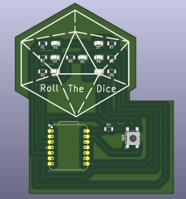
Since I knew I was going to eventually be updating the wiring, I decided to get artistic and play around with the shape of the board.
While it's not a huge difference, I do like the d20 design I made using the edge cut and the silkscreen.
I tried to align the center LED to be in the center of the d20 design so that it would have a cool effect when you roll a 1. The other LED’s didn't really line up super well, but I may try and space them out into the different parts of the d20 I layed out on the silk screen.
I am thinking something along the lines of this LED pattern formation.
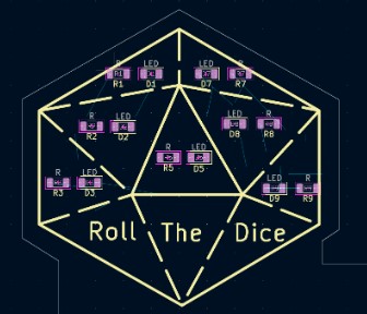
I will have to adjust the d20 shape a bit to better align the LEDs but I think it will be a cool look when I rewire everything.
Code Update
Updated my code in the WokWi simulation
I took the time to update my code on my Wokwi simulation so that I know this board wiring formation will work if I decide to mill it.
I am actually kind of excited for this board project, and I do plan to mill this one as practice even though it's not required for this week.
The new wiring has each LED on its own pin, so I needed to update my code so that when a dice number is rolled all of the LED's for that number light up. It was a bit tedious to update, but not difficult.
Week 6 Files
In my repo is a zip folder containing files for my week 6.