8. Electronics Production
XIAO ESP32-C3 Development Board
This week I made and tested a microcontroller development board that I designed in Week 6. The workflow covers PCB layout export, G-code generation in Mods CE, CNC milling on the KEXU machine, component soldering, and functional verification. I also participated in the group assignment to characterize our lab's in-house PCB production process.
Assignment checklist
- Linked to the group assignment page
- Documented how I made the toolpath
- Documented how I milled, stuffed, and soldered the board
- Documented that my board is functional
- Explained problems and how I fixed them
- Uploaded source code and included a hero shot of my board
Assignment Tasks
- Individual: Make and test a microcontroller development board that you designed.
- Extra credit: Make it with another process — I also ordered a revised board from JLCPCB.
- Group: Characterize the design rules for in-house PCB production.
Group Assignment
As a group we characterized how PCBs are made at Chaihuo — both in-house on the KEXU CNC and through a board house (JLCPCB). We tested machine parameters, documented the milling workflow, and compared milled vs. manufactured boards.
Week 8 Group Assignment — Chaihuo Fab Lab
What I learned from the group work
| Topic | Key takeaway |
|---|---|
| Design rules | In-house milling needs ≥ 0.38 mm trace/space. Wider power buses are more reliable than thin signal traces after milling. |
| Z zero | A board that is not flat or a Z zero that is slightly off produces shallow traces or cuts into the sacrificial layer. The paper-drag test is critical. |
| Mods workflow | KiCad Gerber → PNG → Mods CE → G-code bridges design and the CNC controller. Always simulate before cutting copper. |
| Browser choice | Use Chrome or Edge with Mods. Some browsers produce bad toolpaths with unwanted dots. |
| Post-milling | Clean the board (scrape loose copper, wash off FR-4 dust) before soldering — oils and dust cause bad joints. |
CNC Machine for Electronics Production
Last week I studied CNC machining on a larger machine. The same principles — fixturing, tool selection, origin setup, and G-code execution — apply to the smaller CNC mill we use for electronic production.
At Chaihuo Fab Lab I milled my board on the KEXU (刻序) benchtop CNC. PNG images are exported
from KiCad Gerbers, toolpaths are generated in Mods CE, and the resulting .nc files are loaded
directly into the machine controller.
Tools used for this board
| Operation | Tool | Notes |
|---|---|---|
| Trace isolation | 40° #502 V-bit | Only V-bits in our lab inventory are suitable for PCB tracing |
| Outline cut | 1.5 mm ball-end mill | Used to cut the board free from the copper-clad sheet |
- Place a sacrificial backing plate (wood) under the copper board.
- Secure both the base and the board with double-sided tape.
- Set the origin carefully at the start — confirm tool position before pressing start.
- Wear a mask and goggles — FR-4 dust is fine and should not be inhaled.
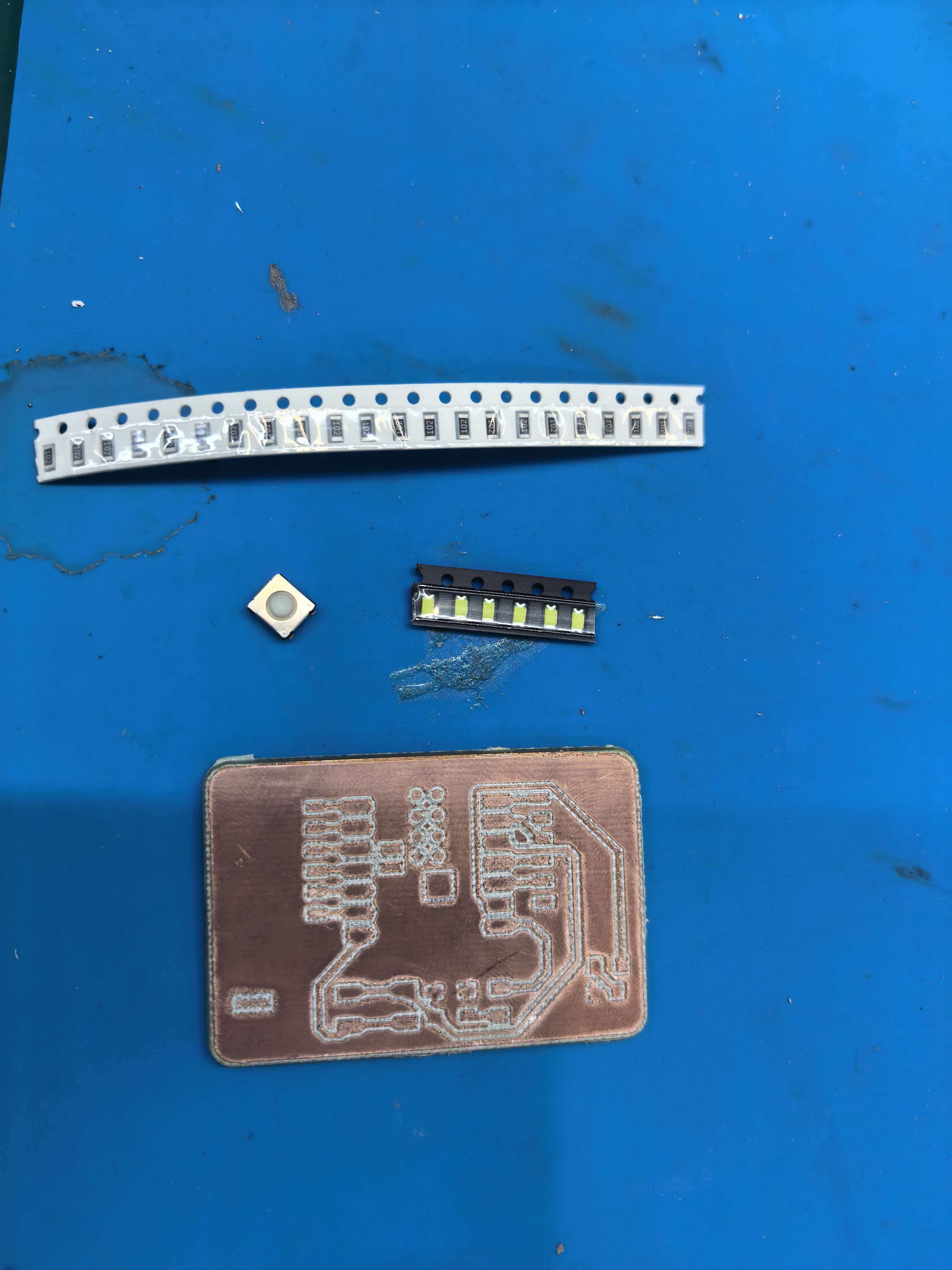
Preparation — Components & Circuit
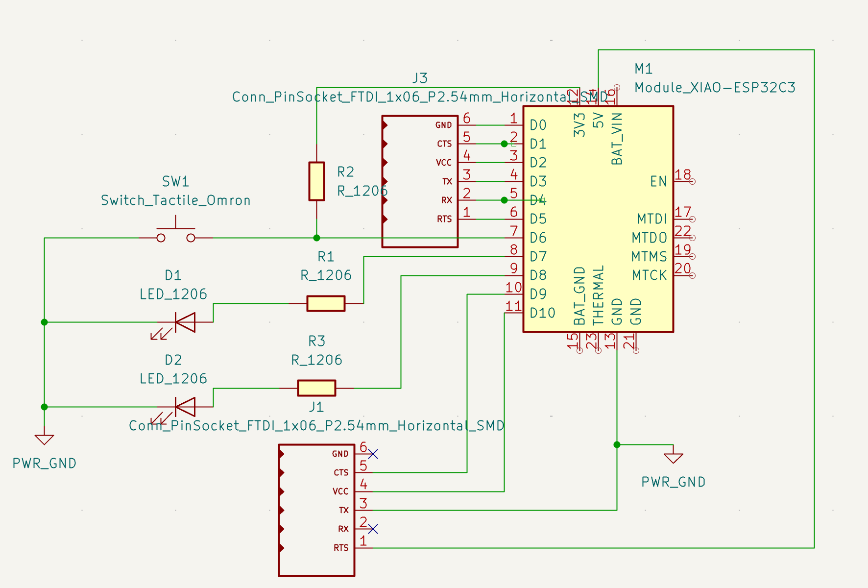
I designed this development board in Week 6, using the Fab Academy KiCad library. The carrier hosts a Seeed Studio XIAO ESP32-C3 with breakout headers, a push-button, and LEDs for I/O testing.
Bill of materials
| Component | Quantity | Ref on board |
|---|---|---|
| Seeed Studio XIAO ESP32-C3 | 1 | U1 |
| CONN HDR 6POS 0.1" TIN SMD | 2 | J1, J2 — left & right pin breakouts |
| Tactile Switch SPST-NO Top Actuated SMD | 1 | SW1 |
| LED 1206 SMD | 2 | D1, D2 |
| RES 1 kΩ 1% 1206 | 2 | Current-limiting resistors for LEDs |
| RES 10 kΩ 1% 1206 | 1 | Button pull-up (revised design) |
G-code Generation in Mods CE
I followed the Mods CE PCB milling workflow to go from KiCad design to CNC toolpaths. PNG images are required because they are lossless — JPEG compression can break fine trace geometry.
Step 1 — Export Gerber from KiCad
- In KiCad PCB Editor: File → Fabrication Outputs → Gerbers.
- Selected
F.Cu(front copper) andEdge.Cuts(board outline). - Exported the front copper and edge-cut Gerber files.
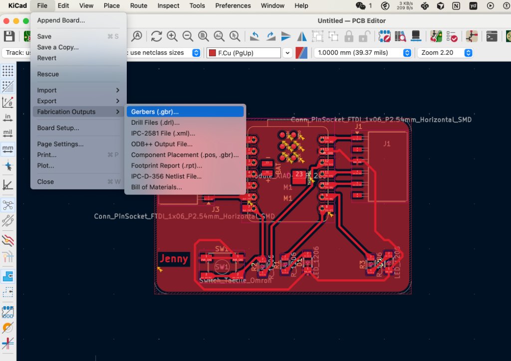
KiCad fabrication output — selecting layers for Gerber export.
Step 2 — Convert Gerber to PNG
- Uploaded the Gerber files to Gerber2Png.
- Set up the trace layer and edge layer, then exported PNG files.
- Verified that traces appeared as white lines on a black background (correct polarity for Mods).
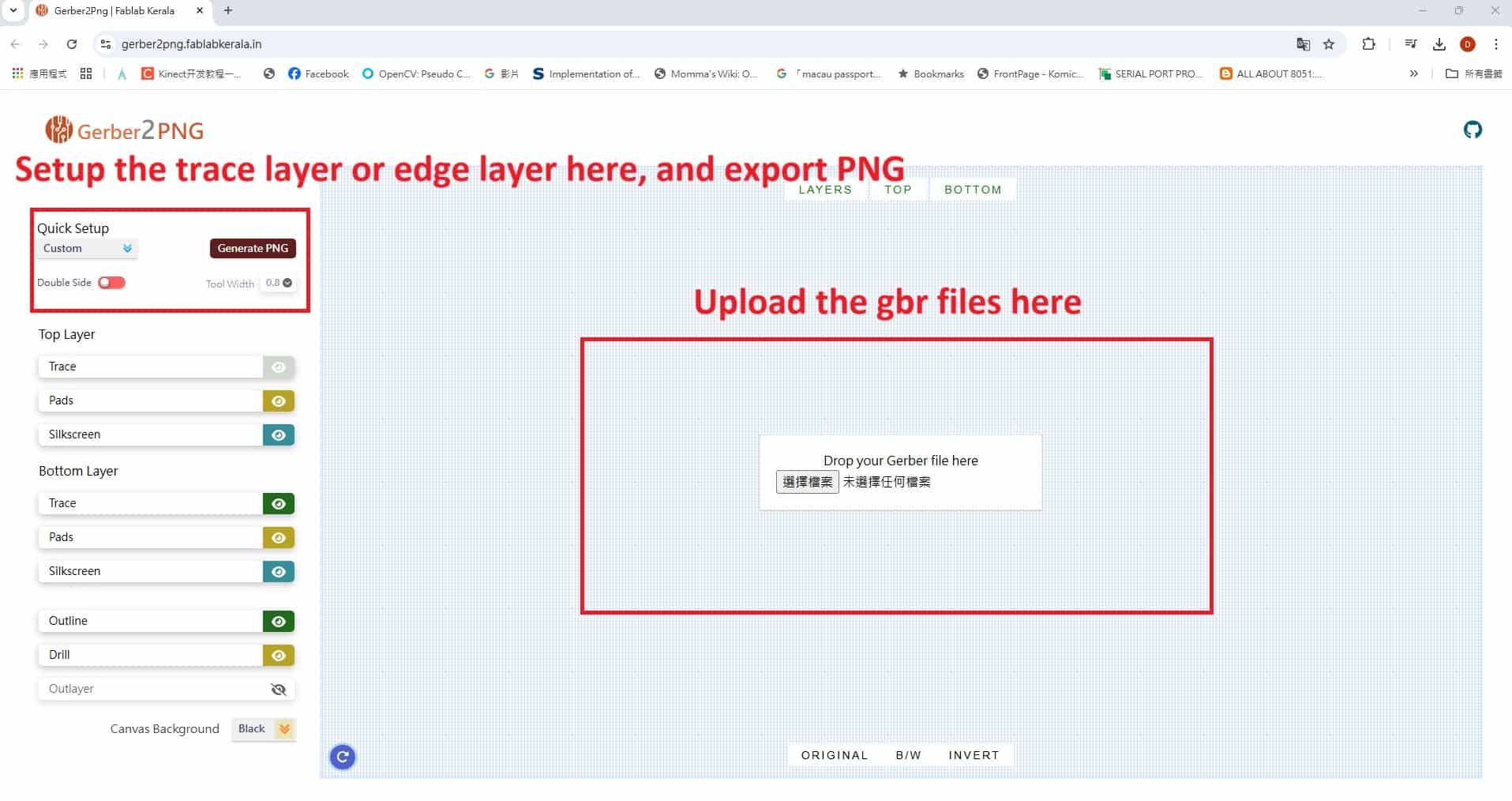
Gerber2PNG — upload Gerber files and configure layer export.

Exported traces_toplayer_0.png and outline_toplayer_2.png ready for Mods.
Step 3 — Generate toolpaths in Mods CE
- Opened Mods CE in Chrome → right-click → program → Open Program.
- TRACES — This tool works with both SVG (top section) and PNG (bottom section). I used PNG. Click select png file and select
traces_toplayer_0.png. - The traces image appears in the preview window.
- Set the PCB milling preset to 40°#502 V-bit.
- Enable file output by turning the On/Off toggle ON.
- In Mill Raster 2D, click calculate to generate the G-code.
- Review the 3D preview simulation to verify the toolpath.
- Click save file to download
traces_toplayer_0.png.nc. - Outline pass: reloaded Mods, loaded
outline_toplayer_2.png, set ball-end / end-mill parameters → Calculate → saved the outline file.
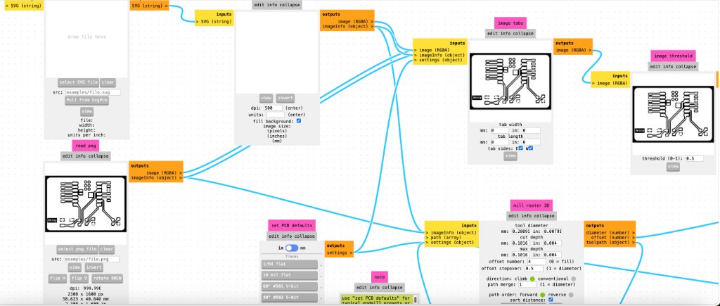
Mods CE — PCB milling preset and Mill Raster 2D configuration.
3D preview of the trace isolation toolpath before saving the G-code file.
Machine parameters used
| Parameter | V-bit (tracing) | Ball-end mill (outline) |
|---|---|---|
| Feed speed | 4 mm/s | 4 mm/s |
| Spindle speed | 14,000 rpm | 14,000 rpm |
| Offset number | 4 | 4 |
| Offset stepover | 0.2 mm | 0.2 mm |
| Cut depth | 0.23 mm | 0.45 mm |
| Tool | 40° #502 V-bit (0.3 mm effective) | 1.5 mm ball-end mill |
CNC Setup & Milling
Fixturing the copper board
- Placed the single-sided copper-clad board (1.6 mm FR-4) on the sacrificial wooden backing plate.
- Secured it with double-sided tape and checked that the board was flat across the work area.
Tool change & zeroing
- Installed the V-bit for tracing and tightened it with the provided wrenches.
- Set X/Y at the front-left corner of the copper board.
- Set Z using the paper-drag test — lower until the bit just scratches the tape, then set Z = 0.
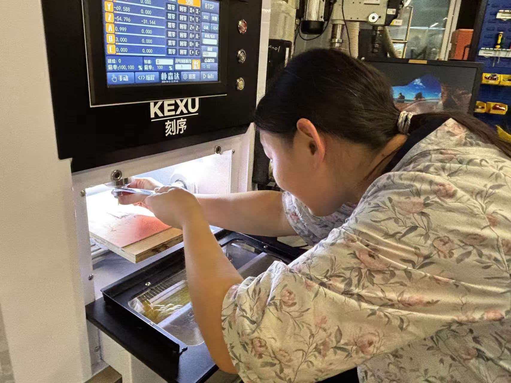
Installing and tightening the milling tool inside the KEXU CNC work chamber.
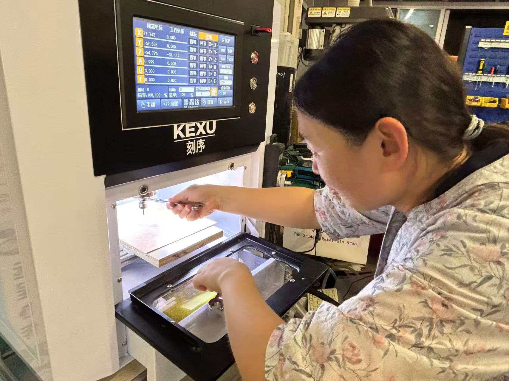
Copper-clad board secured on the sacrificial layer, ready for origin calibration.
Start milling
- Loaded
traces_toplayer_0.png.ncfrom USB (FAT32, no hyphens in filename). - Moved the tool above the origin point before pressing start.
- Ran the trace program first at 14,000 rpm spindle speed.
- Swapped to the ball-end mill, re-zeroed Z, loaded the outline G-code, and cut the board free.
PCB trace milling on the KEXU CNC — V-bit isolating copper traces on the development board.
Post-processing
After milling there were burrs on the board surface. I removed them with sandpaper, then washed the board with soap and water to remove oils and FR-4 dust before soldering.
Problems and How I Fixed Them
On my first test I milled in different areas of the copper board but forgot to reset Z0 when moving to a new region. In some areas the V-bit did not cut deep enough, leaving thin copper bridges between traces.
Re-zeroed Z carefully using the paper-drag test at the chosen cutting region, then re-ran the trace G-code. After finding a flat area on the board, the second pass produced clean trace isolation.
My first attempt at generating G-code in Mods using an unsupported browser produced a toolpath with stray dots and irregular patterns around pad areas.
Switched to Chrome as recommended in the group documentation. Regenerated the toolpath — the simulation looked clean with no stray dots.
This was my first time soldering 1206 SMD components. The tiny parts were difficult to hold in place without tweezers, and I accidentally bridged two adjacent XIAO castellated pads.
Used fine tweezers to position each component, tacked one corner first, then flowed solder on the remaining pads. Removed the bridge with solder wick and flux, then verified continuity with a multimeter.
After soldering the milled board, the button input did not work reliably. I checked the circuit again and found that the pull-up resistor was not correctly connected to the button net in the original layout.
I corrected the schematic and PCB in KiCad, adding a proper pull-up resistor to the button circuit, then ordered a revised board from JLCPCB. The manufactured board passed all functional tests.
Revised circuit — pull-up resistor correctly connected to the button input.
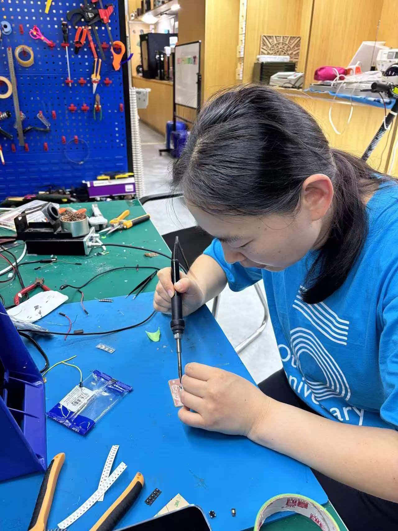
Soldering
After milling and cleanup I soldered all components onto the board. I worked at the Fab Lab bench with a fume extractor, multimeter, and fine-tip soldering iron.
- SMD passives first: resistors, LEDs, and the tactile switch — tacked one corner, then soldered remaining pads.
- Headers: inserted both 1×6 pin headers, tacked one pin each for alignment, then soldered all pins.
- XIAO module last: placed the ESP32-C3 on its castellated pads, aligned the USB-C port flush with the board edge, and soldered each pad carefully.
- Inspection: checked all joints under magnification for bridges and cold joints.
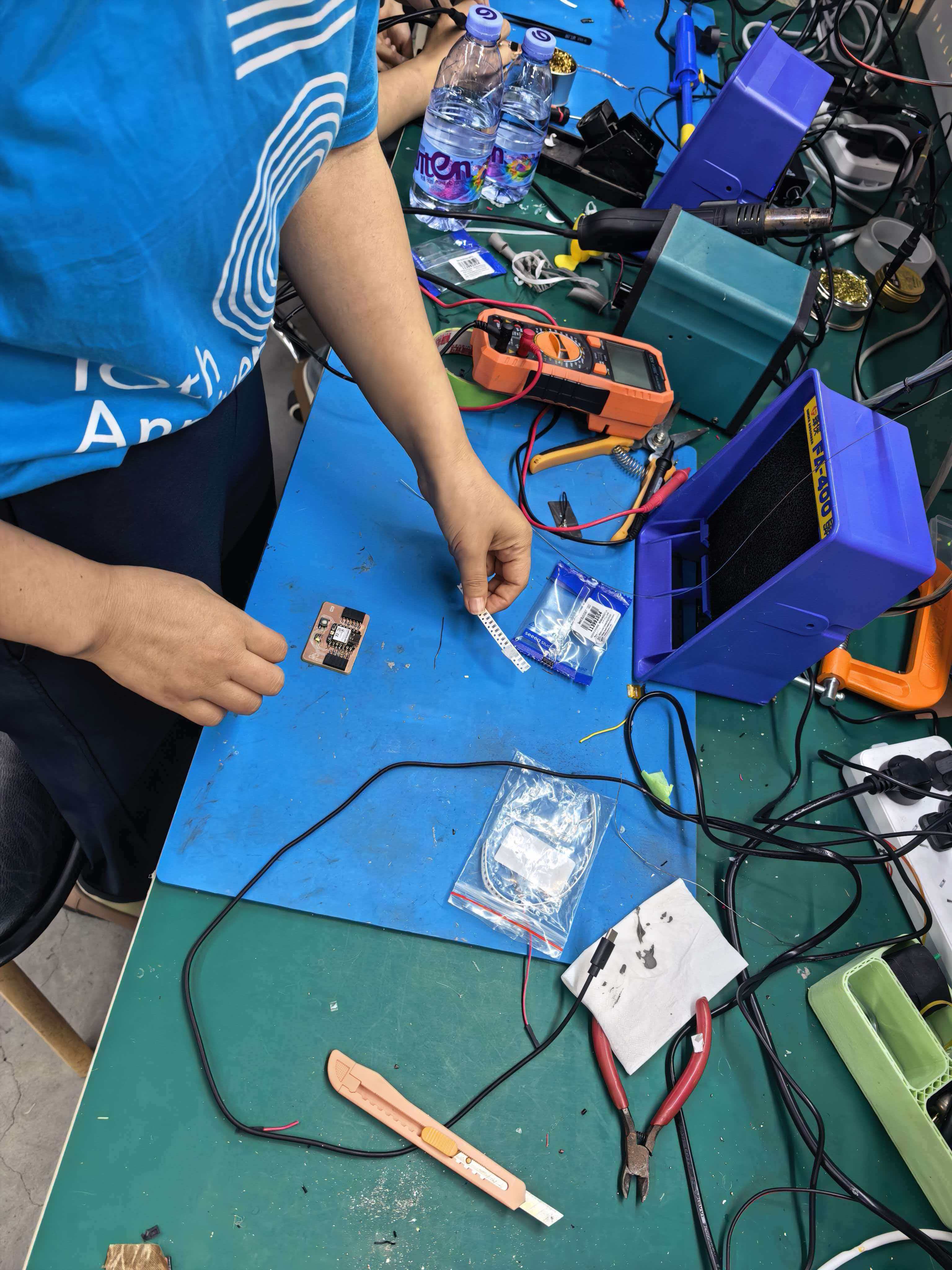
Preparing SMD components and the milled board at the soldering station.
Soldering the XIAO ESP32-C3 module — tweezers are essential for positioning small SMD parts.
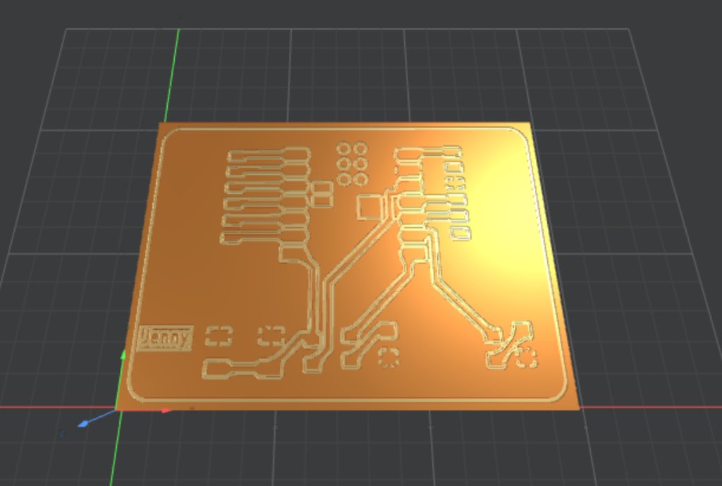
Milled board after soldering all components.
Board Testing
Pin mapping (revised board)
On the corrected HelloworldNew board, the button and LEDs connect to these XIAO ESP32-C3 pins:
| Pin | Connected to | Direction | Notes |
|---|---|---|---|
D7 | Tactile switch (SW1) | Input | Uses INPUT_PULLUP — reads LOW when pressed |
D8 | LED 1 (D1) | Output | Active HIGH through 1 kΩ resistor |
D9 | LED 2 (D2) | Output | Active HIGH through 1 kΩ resistor |
What the test program does
- Setup: starts USB serial at 115200 baud, configures D7 as input with internal pull-up, and sets D8/D9 as outputs (both off).
- Loop: reads the button state every 10 ms.
- On press: when the button goes from not-pressed (
HIGH) to pressed (LOW), waits 50 ms for debounce, then toggles both LEDs together. - Serial output: prints
LED ONorLED OFFto the serial monitor so I can confirm the button is detected.
How to upload
- Open HelloWorldWeek8.ino in Arduino IDE.
- Board:
XIAO_ESP32C3· Port: the USB-C serial port · Enable USB CDC On Boot. - Upload, then open Serial Monitor at 115200 baud.
- Press the button — both LEDs should toggle; serial monitor should print the new state.
Test firmware
Full source: HelloWorldWeek8.ino
/*
 * HelloWorldWeek8.ino
 * Button on D7 (INPUT_PULLUP) — press reads LOW
 * LEDs on D8 and D9 — toggle together on each press
 */

#define SWITCH_PIN  D7
#define LED1_PIN    D8
#define LED2_PIN    D9

bool ledState = false;
bool lastButtonState = HIGH;

void setup() {
  Serial.begin(115200);
  pinMode(SWITCH_PIN, INPUT_PULLUP);
  pinMode(LED1_PIN, OUTPUT);
  pinMode(LED2_PIN, OUTPUT);
  digitalWrite(LED1_PIN, LOW);
  digitalWrite(LED2_PIN, LOW);
}

void loop() {
  bool currentButtonState = digitalRead(SWITCH_PIN);

  // Detect falling edge: button just pressed (HIGH → LOW)
  if (lastButtonState == HIGH && currentButtonState == LOW) {
    delay(50);  // debounce
    ledState = !ledState;
    digitalWrite(LED1_PIN, ledState ? HIGH : LOW);
    digitalWrite(LED2_PIN, ledState ? HIGH : LOW);
    Serial.println(ledState ? "LED ON" : "LED OFF");
  }

  lastButtonState = currentButtonState;
  delay(10);
}
Test results
- Multimeter: no short between 5V and GND.
- USB-C connected — XIAO power LED lit up.
- Button press toggles both LEDs; serial monitor prints
LED ON/LED OFF.
Result: The revised JLCPCB board passed all tests.
Hero Shot
The finished XIAO ESP32-C3 carrier board — designed in KiCad, first milled on the KEXU CNC, then revised and manufactured by JLCPCB after fixing the pull-up resistor connection.
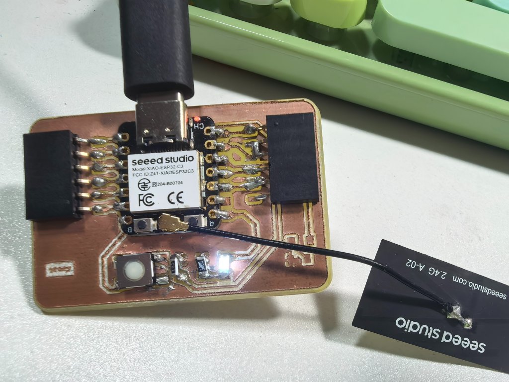
Button press toggles the LEDs; serial monitor prints the button state over USB.
Reflection & Key Takeaways
- Design for your machine. Trace width and clearance must match the milling process, not just KiCad DRC defaults.
- Z zero is everything. Forgetting to reset Z0 when moving to a new board region was my biggest milling mistake.
- Simulate before cutting. Mods 3D preview and Wokwi simulation both caught issues before wasting copper or ordering a bad board.
- Check the schematic, not just the layout. The pull-up resistor bug only became obvious after soldering — a continuity check against the schematic would have caught it earlier.
- Two fabrication methods teach different lessons. Milling taught me fixturing and Z-height; JLCPCB gave me a reliable board to verify the corrected circuit.
Source Files
All design, manufacturing, and firmware files for this assignment:
KiCad design
| File | Description |
|---|---|
| HelloworldNew.kicad_sch | Schematic — revised design with pull-up resistor fix |
| HelloworldNew.kicad_pro | KiCad project file |
| HelloWorldWeek6-F_Cu.gbr | Front copper Gerber (original Week 6 design, used for milling) |
| HelloWorldWeek6-Edge_Cuts.gbr | Board outline Gerber (original Week 6 design) |
| Week 6 documentation | Original KiCad design workflow |
Milling files (PNG → G-code)
| File | Description |
|---|---|
| traces_toplayer_0.png | Trace layer image — input to Mods CE for isolation milling |
| outline_toplayer_2.png | Board outline image — input to Mods CE for cutout |
| drills_toplayer_1.png | Drill layer image |
| traces_toplayer_0.png.nc | Generated trace G-code — loaded on KEXU CNC to mill copper traces |
Firmware (source code)
| File | Description |
|---|---|
| HelloWorldWeek8.ino | Arduino test program — button on D7 toggles LEDs on D8/D9, prints state over serial |