PCB Design
Learning Background
This week, I began designing my first custom PCB(Printed Circuit Board) for my final project, using KiCad as my primary EDA(Electronic Design Automation) tool. KiCad is a free, open-source suite for schematic capture and PCB layout.
Before diving into PCB design, I realized my fundamental knowledge of circuits was very poor, I had been mostly "copying schematics" without truly understanding the flow of current, voltage, and resistance. So I started with basic electronics fundamentals:
- I reviewed SparkFun's tutorial on Voltage, Current, Resistance, and Ohm's Law, which clarified why we need current-limiting resistors for LEDs and pull-up/pull-down resistors for switches.
- I also skimmed Getting Started in Electronics (available on Archive.org), which uses hand-drawn diagrams to explain component symbols,perfect for understanding schematics visually.
Next, I set up my KiCad environment:
- Downloaded the official Fab Academy KiCad libraries from GitLab.
Why Fab libraries? They ensure global compatibility across Fab Labs—ATtiny, ESP32, XIAO modules are pre-configured, eliminating custom library creation.
Then I get to learn about:
- .sym files: Schematic symbol libraries (e.g., resistor zigzag, LED arrow-bulb), used for drawing logical circuits.
- .pretty folders: Footprint libraries (e.g., 1206 resistor pad spacing), used for physical PCB layouts.
In KiCad, I configured:
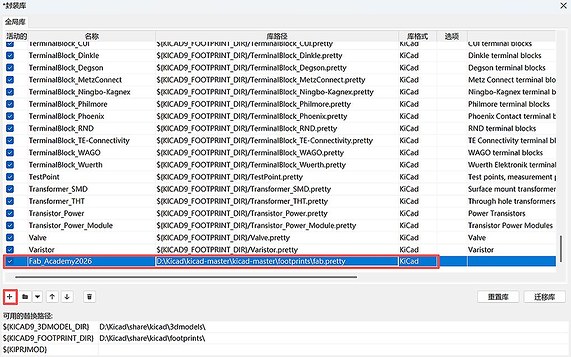
- Preferences → Manage Symbol Libraries → Added fab.kicad_sym.
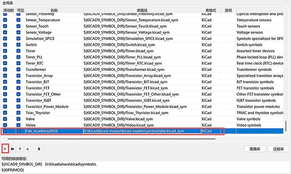
- Preferences → Manage Footprint Libraries → Added fab.pretty.
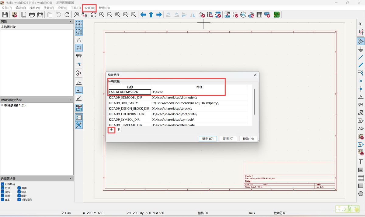
- Settings → Configure Paths → Linked Fab library path for proper 3D rendering.
First Attempt: Schematic Design
Inspired by alumni like Lei Feng and CHON KIT KUOK's Week 6 docs, I designed a simple "Hello World" board for my project:
- Core: Seeed XIAO ESP32C3
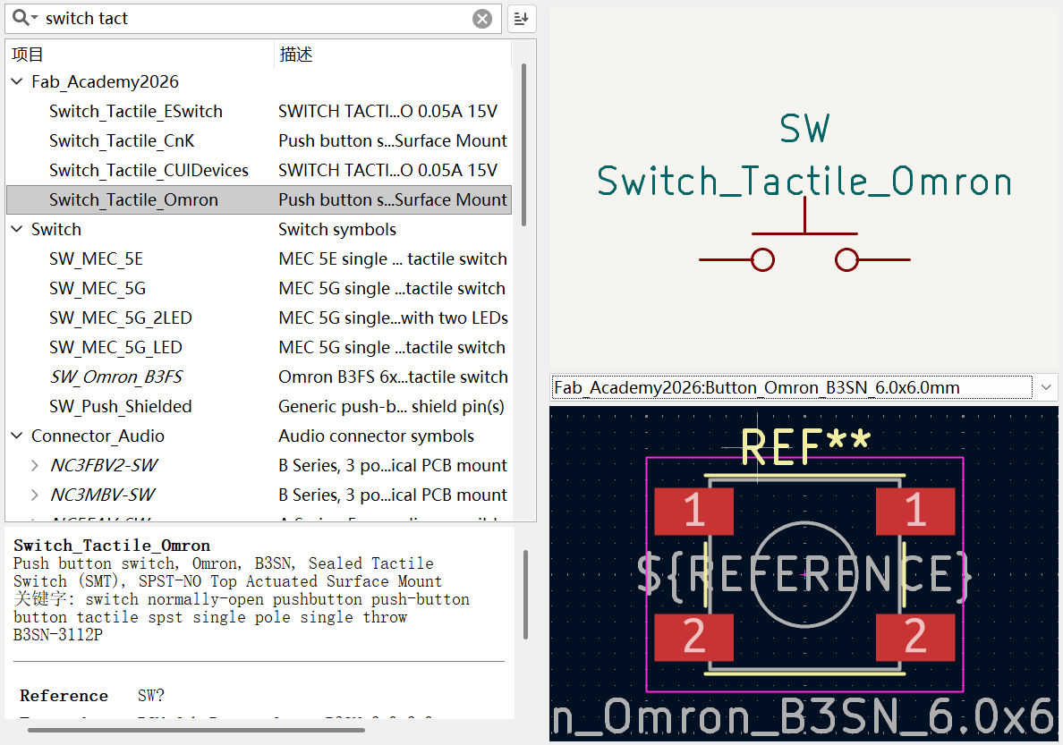
- Input: One switch (for pull-ring mechanism)
- Output: One LED (for testing)
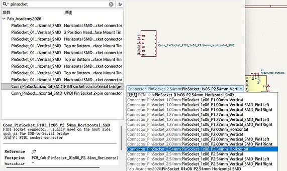
- Expansion: Two 6-pin headers (for future Dupont connections to e-ink driver board)
In KiCad's Eeschema:
Create a project and import the library
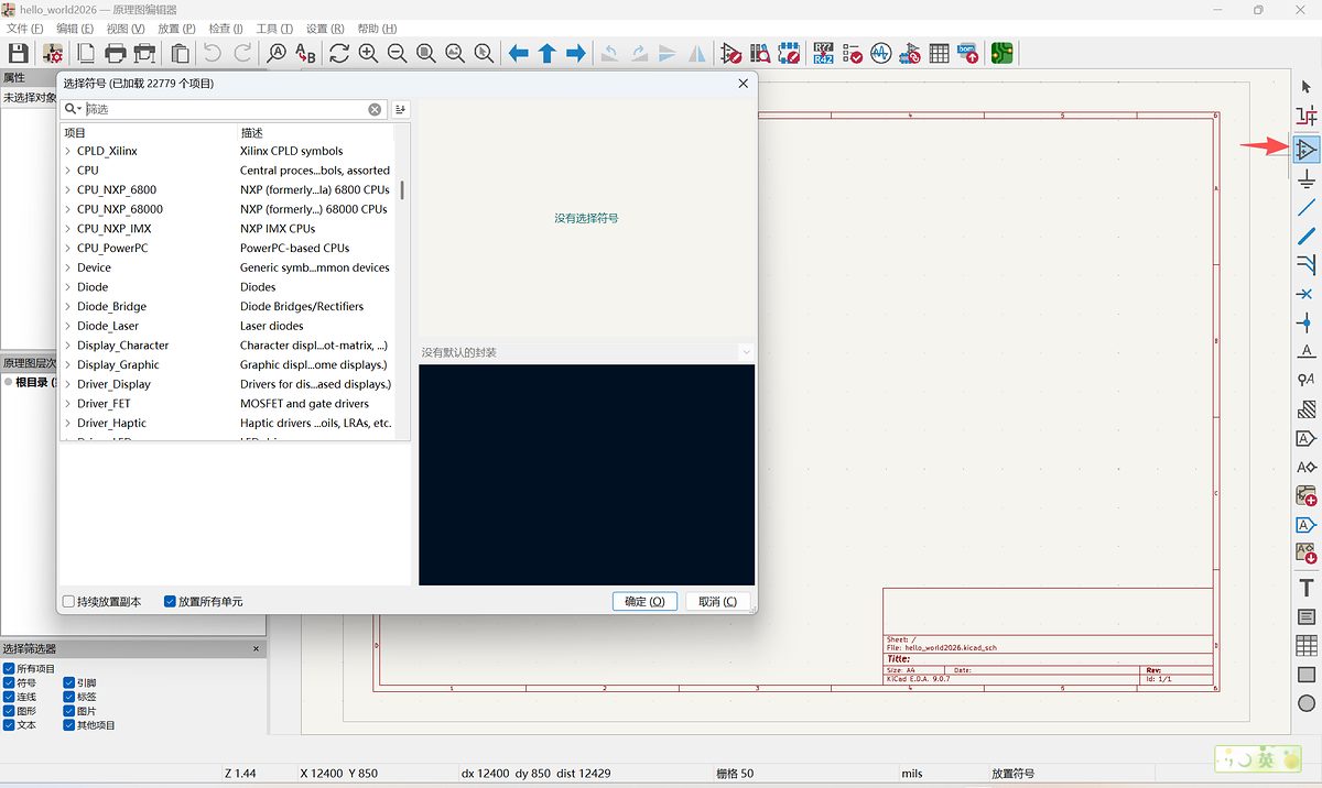
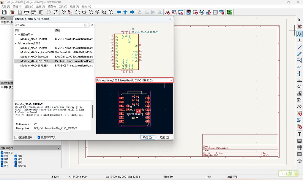
1.Placed XIAO ESP32C3 symbol from Fab library.
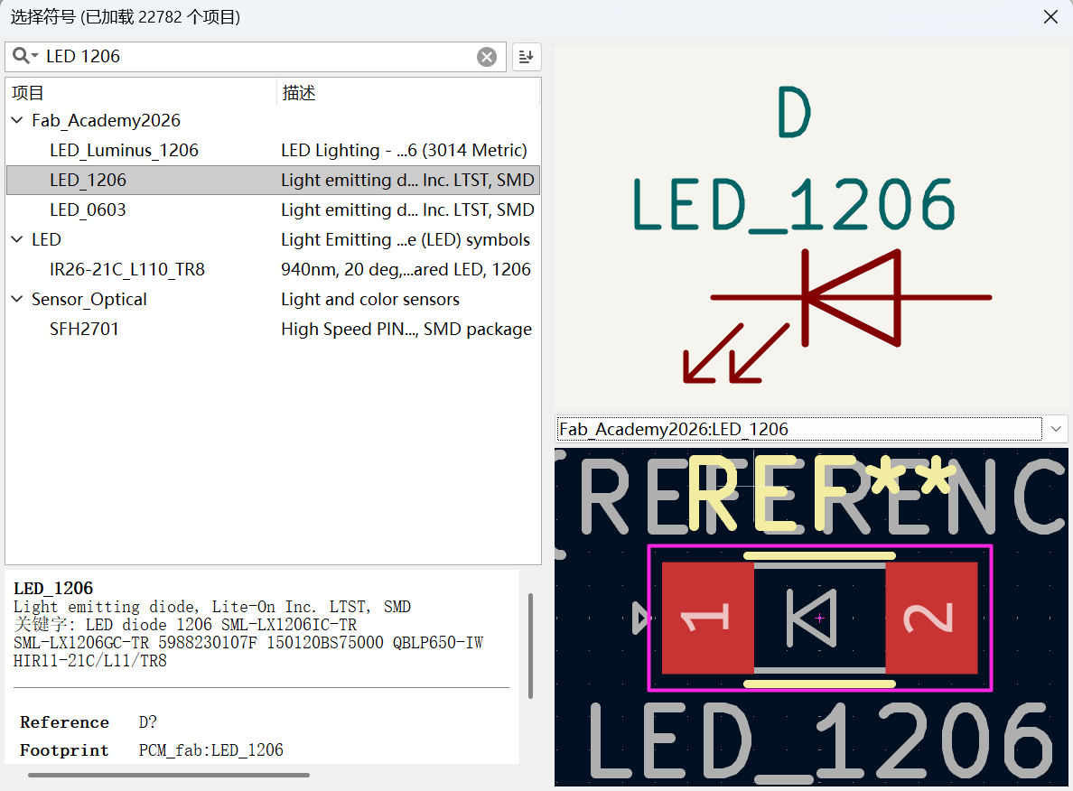
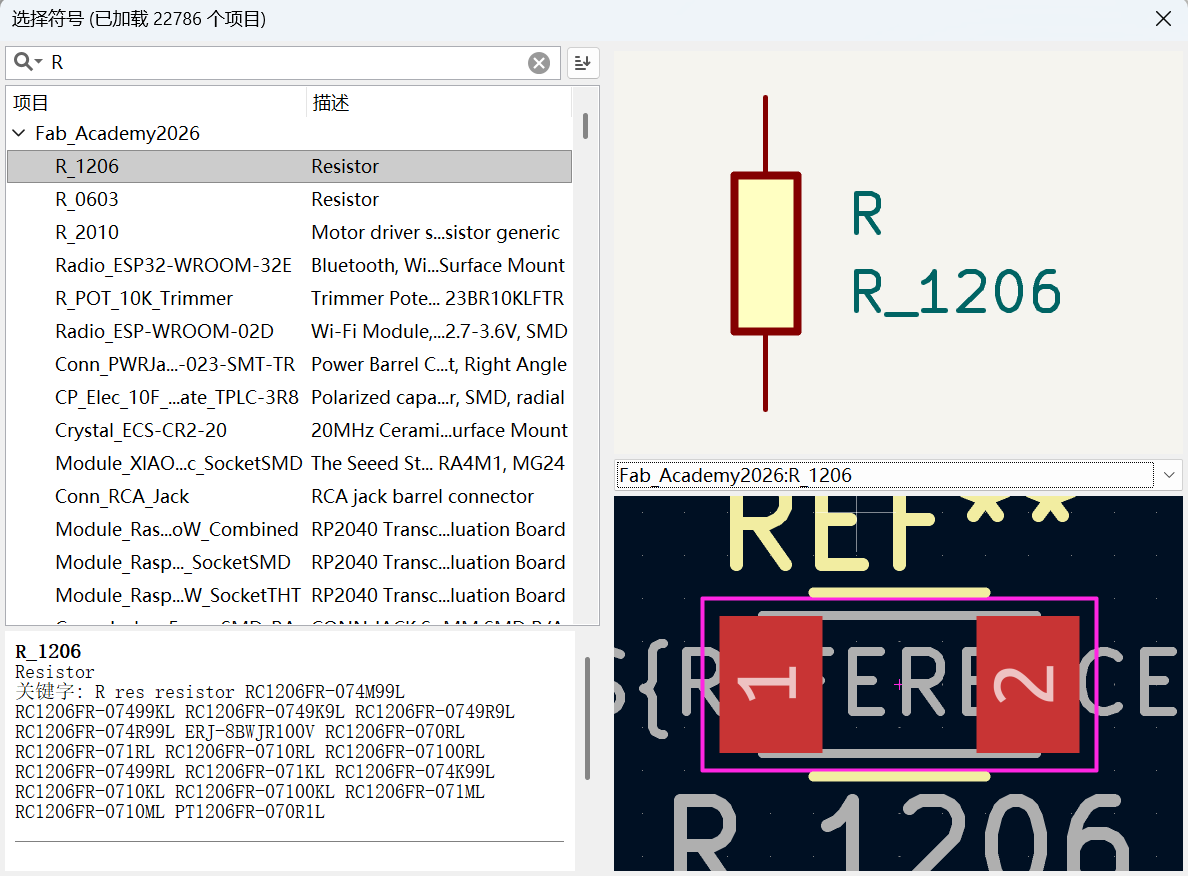
2.Added components: 1206 LED, SPST switch, 6-pin sockets.
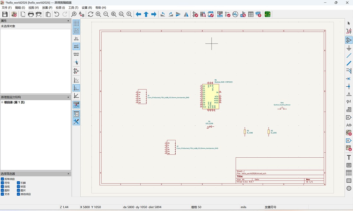
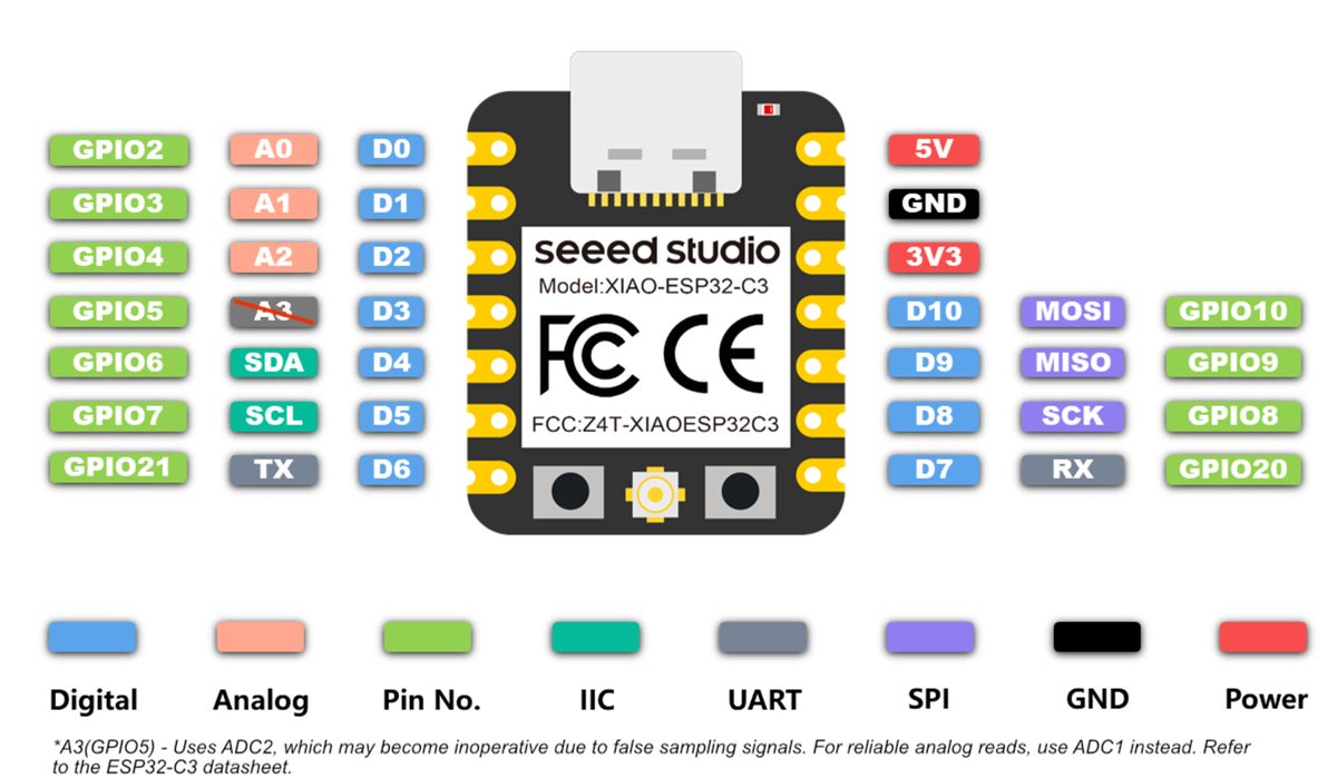
3.Referenced XIAO ESP32C3 Wiki for pins:
- One GPIO for switch input.
- One GPIO for LED output.
- Others routed to headers for modularity (e.g., SPI/I2C for e-ink).https://wiki.seeedstudio.com/XIAO_ESP32C3_Getting_Started/
4.Added two resistor to switch (prevents direct short-circuit, protects MCU).
5.Ran ERC (Electrical Rules Check) to fix power/ floating pin issues.
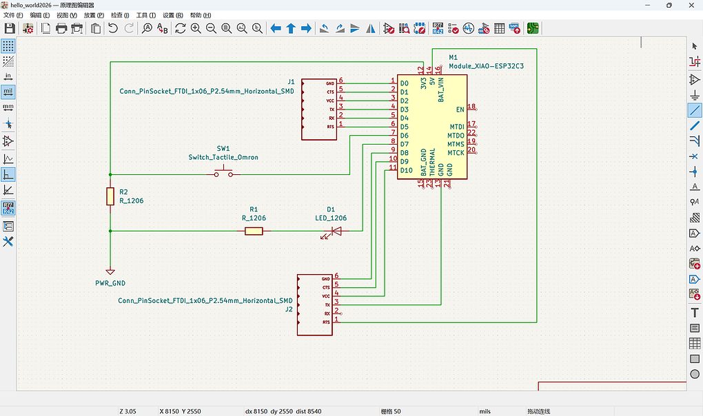
Wire all together, the schematic finished:
Draw PCB Layout
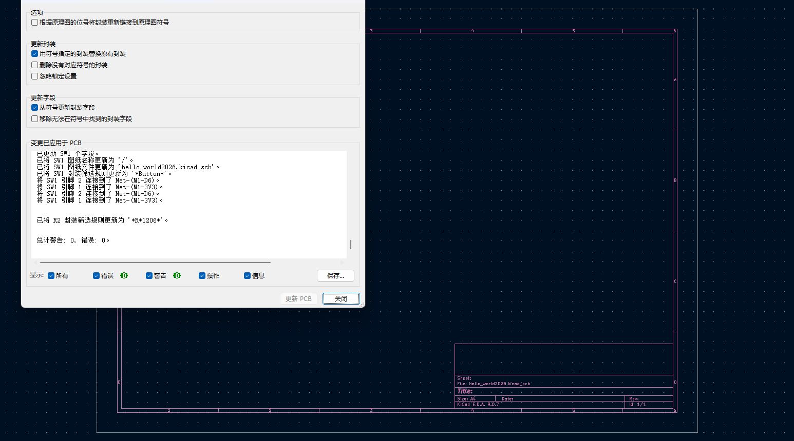
Click the Tools to Update the PCB, it shows one error of my resistor, and when I replace the second one, it looks well:
Then I got the first look of my PCB
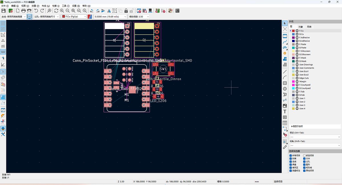
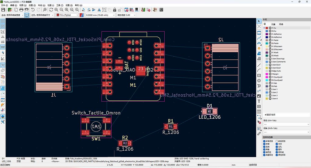
Change the order to make it smooth to route:
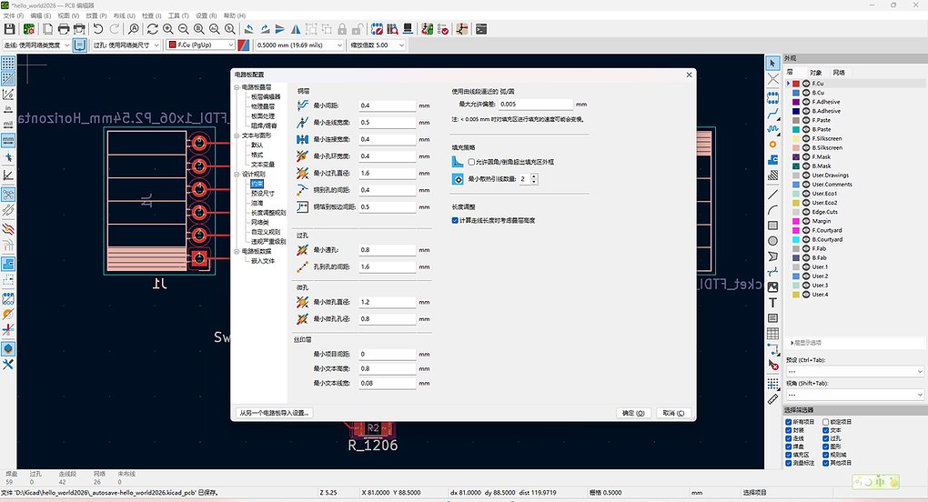
Adjust the PCB design rules. Better before route,or we will do the step again.
Use Route tool to link the routes.
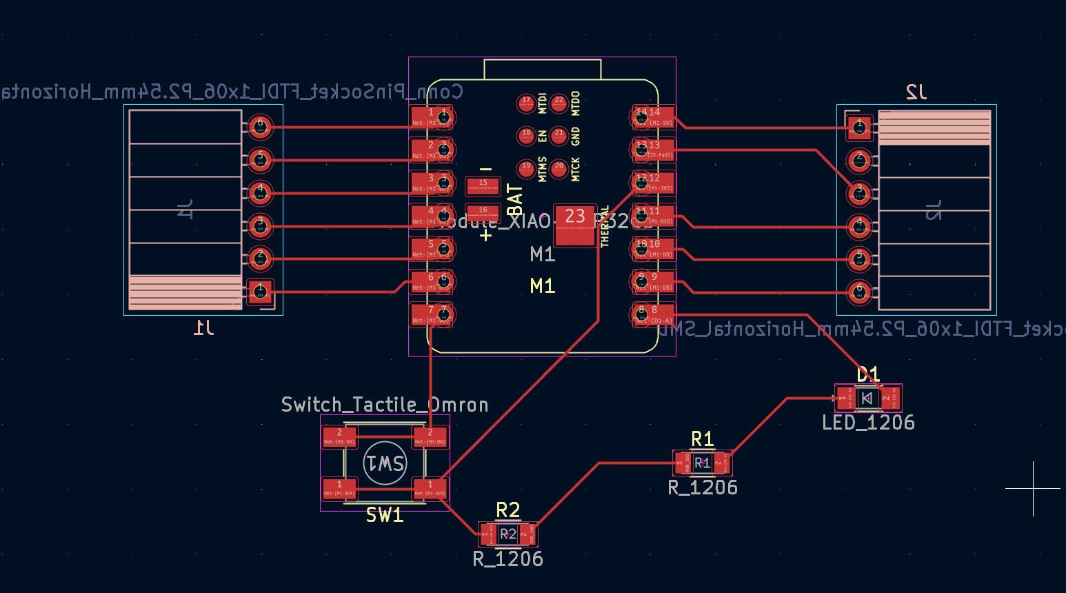
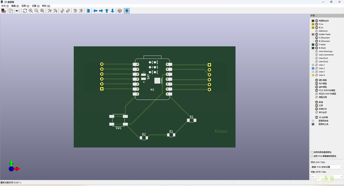
After finishing the trace layer, change to cut layer (Choose Cut Edge) and draw the boarder of the circuit board, use rectangle to draw the white frame. And I labelled my name on it:
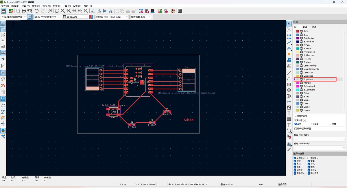
3D viewer can be opened in PCB editor.