

Software & Tools
Arduino IDE
Sketch editing, board package management, uploading, and serial monitoring.
Version 2.3.7
Open Source (GNU AGPLv3)


LPKF Circuit Pro
Gerber import, layer mapping, process planning, and toolpath generation for PCB milling.
2.5 PM
Lab machine software license
PCB Milling
Maintenance
Before the LPKF ProtoMat S63 can be used, it must be maintained. This is roughly once a month and takes about 20 minutes. We have a dedicated maintenance kit consisting of a wrench specifically for the LPKF head, lubricant, and special cleaning tubes.
First, any tools that may be in the milling head must be removed. Then, using the wrench, the milling head can be loosened. All milling residue must be cleaned out using a cloth and some isopropanol. The inner threads of the tool holder should also be cleaned, where the cleaning tubes help. Once the tool holder is cleaned, new lubricant can be applied. Use about the size of a pea and spread with a cloth. Then the wrench is used again to reattach the tool holder to the machine.
Creating the PCB
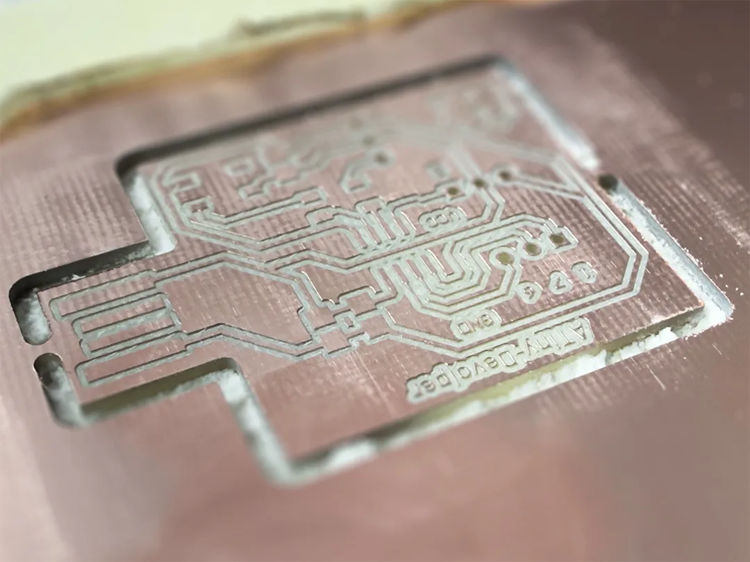
You can find a detailed step by step walkthrough of the milling setup process with pictures right here. But to summarize, you first have to place the PCB to be milled in the machine and additionally secure it with masking tape. The machine uses vacuum suction similar to the CNC machine from last week, but there is also a sacrificial board to prevent damage to the machine. Because of this, the suction strength is somewhat limited, and the board should be secured to prevent shifting.

The copper boards should only be handled with gloves. Finger grease can affect conductivity and potentially cause short circuits or other PCB errors.
In the LPKF Circuit Pro PM 2.5 software, a new project can be created. We have presets for different PCB types available, e.g., single-layer and double-layer boards. Here, I selected single-layer. The Gerber files can now be added. The ZIP file should be extracted, and the files imported using the Import button in the LPKF software. If there are additional layers that should not be milled, they can simply be deselected.
To let the machine know what to mill, each file/layer must be assigned to its operation. Usually, this is easy as the files are already named according to the layers. For example: Gerber_Top_Layer => TopLayer
Layer Explanation
| Layer Name | Altium Ext. | LPKF Operation | Required |
|---|---|---|---|
| PCB Stack Operations | |||
| Top Silkscreen (Top Overlay) | .GTO (Gerber Top Overlay) |
Contains designators, logos, and part labels; useful for debugging and manual assembly, not processed by LPKF | Optional |
| Top Paste Mask | .GTP (Gerber Top Paste) |
Defines solder paste areas for SMD reflow; not applicable for LPKF milling workflow | — |
| Top Solder Mask | .GTS (Gerber Top Solder Mask) |
Defines lacquer-protected areas; LPKF boards are typically uncoated, not applied | — |
| Top Copper Layer | .GTL (Gerber Top Layer) |
Isolation Milling — the router mills away copper around traces to define signal paths; core machining step | Essential |
| Substrate / Core | (no file) | FR4 or RF4 laminate with copper cladding on one or both sides; raw board material used as-is | No operation on that layer |
| Bottom Copper Layer | .GBL (Gerber Bottom Layer) |
Isolation Milling (mirrored) — same process as Top Layer; board is physically flipped and file must be mirrored in LPKF CircuitPro to compensate | Essential, Double-sided only |
| Bottom Solder Mask | .GBS (Gerber Bottom Solder Mask) |
Same logic as Top Solder Mask; not used in LPKF prototyping | — |
| Bottom Paste Mask | .GBP (Gerber Bottom Paste) |
Same logic as Top Paste Mask; not used | — |
| Bottom Silkscreen (Bottom Overlay) | .GBO (Gerber Bottom Overlay) |
Contains designators and labels on the bottom side; not processed by LPKF | Optional, Double-sided only |
| Additional Operations | |||
| Drill Layer | .DRL / .TXT (NC Drill File) |
Drilling — LPKF drills all vias, through-hole component holes, and mounting holes; includes plated and unplated sets | Essential |
| Board Outline / Mechanical 1 | .GM1 (Gerber Mechanical 1) |
Contour Routing / Cutting — router follows the board outline path to cut the PCB from the raw laminate panel; performed as the final step | Essential |
For a single-sided prototype, the minimal required files are:
.GTL — Top copper isolation milling
.DRL / .TXT — Drilling
.GM1 — Board cutout
For a double-sided prototype, add:
.GBL — Bottom copper isolation milling
Preview each layer to check correctness. Confirm with OK. For multi-layer boards, fiducials should be added. The LPKF uses an infrared camera to detect them and align the PCB. Place these near existing holes to minimize material waste.
Altium can separate drill files into two types: plated holes (vias, through-hole pads) and unplated holes (mounting holes, slots) — exported as a second file marked DrillUnplated / DrillPlated. In LPKF, both are drilled mechanically the same way, but keeping them separate allows different drill parameters per set.
In Altium Designer, the NC drill output contains all hole drilling data needed for PCB fabrication. This data can be saved in binary format as .DRL or, more commonly, as ASCII drill text format .TXT, which many board houses expect. The output includes tool numbers, X/Y hole coordinates, and hole sizes.
You can export this newer drill file format via File → Fabrication Outputs → NC Drill Files.
Technology and Milling Settings
The Technology dialog allows specific milling details. If the file is prepared correctly, minimal changes are needed. Only in Contour Routing, tabs should be adjusted to hold the board securely, similar to CNC. Vertical or horizontal gaps are recommended. 1mm gap width worked well here. You might also want to add clearance around your traces. You can choose from four different options. For beginners I recommend using the first preset, which will keep the same clearance around all of your traces. Make sure to change the value to 0.8mm to have an easier life soldering your components.
Click Start to calculate the milling process. The LPKF automatically checks required tools. In my case, a 1.8mm spiral drill was missing. The software tells you what tools are needed and which slots you can change. To add a new tool, simply pop off the old one and press the new one in. This is very simple and done within seconds. In that case I added the tool to slot 4 and changed it in the software accordingly. Then, all tools were ready.
Adjust the PCB position manually using the Processing Window to ensure it is correctly placed on the milling bed.
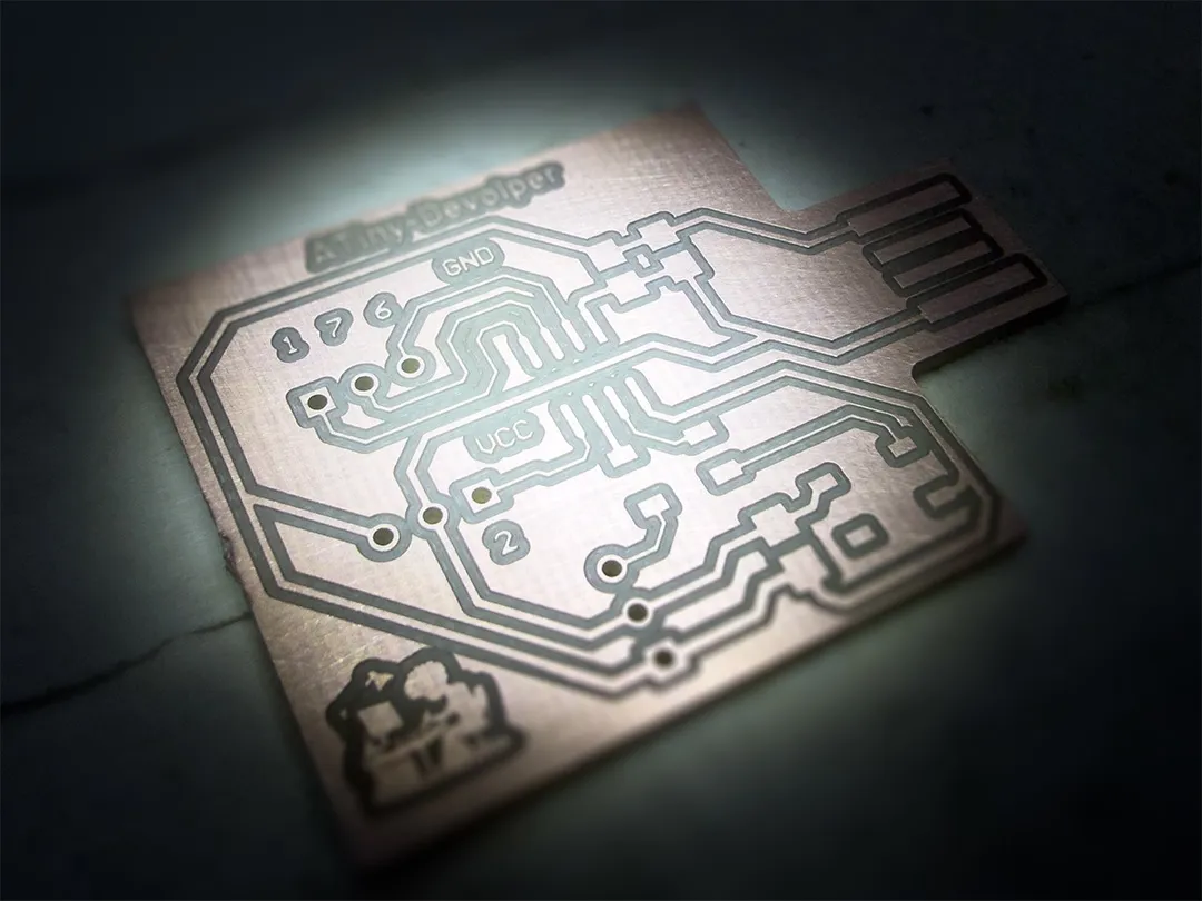
Check material settings: I used a single-sided FR4 board with 18um copper and 1.55mm thickness. The board was 305 x 229 mm.
Start milling in the Operate tab. The machine warms up for two minutes with the tool spinning but stationary. Then it drills holes, mills traces, and finally cuts out the board. The entire process took about 20 minutes.
PCB Finishing
PCB Sanding
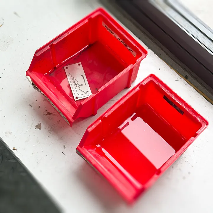
To make the copper areas conductive and clean, the PCB is sanded. Use coarse to fine sponges similar to sandpaper until the PCB shines. Final residue can be removed with isopropanol.
PCB Tinning
Copper oxidizes quickly, potentially causing short circuits. Tinning prevents this, prolonging PCB life. Immerse the PCB in tinning solution, swirl briefly. Copper color changes from brown to silver. Then rinse in water (preferably distilled) and dry with isopropanol.
This step is optional and potentially toxic, so work with care. Alternatively, you can use PCB spray to coat the entire board with a protective layer and then scratch the solder pads open again with a glass-fiber pen. The exposed pads can then be soldered.

Tinning solution must not enter groundwater. Collect carefully in the bottle and do not rinse the container.
PCB Soldering
Now you can move to the soldering step. But first check the board for shorts before soldering.
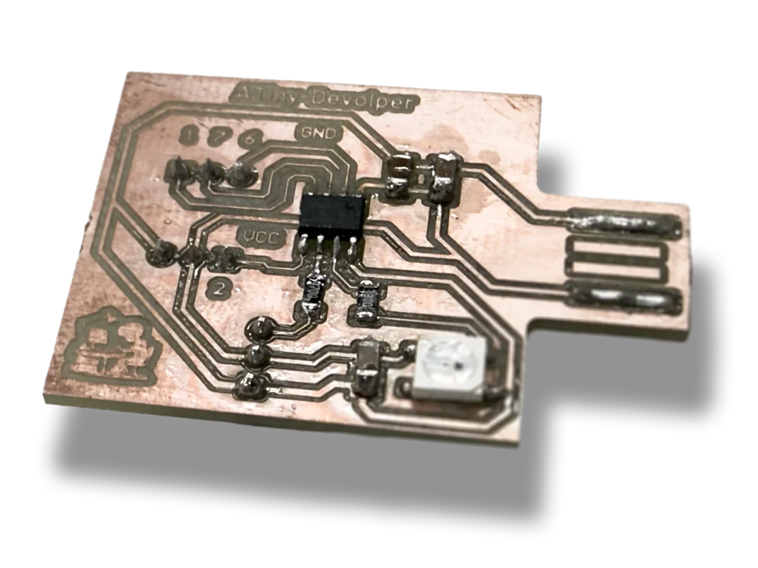
Place and solder components:
Through-hole on the fiber side, feet on pads.
SMD components on the traces side, placed on pads.
Use thin solder (I used 0.8mm) for small parts and a temperature of 290-320°C. Pre-tin the soldering tip for better flow. Then heat the pad and the component leg evenly and apply solder with a small amount of flux.
For an easier time you may want to use a microscope or a third hand to hold your PCB in place. When the soldering takes long make sure to let the components cool for a few moments. This prevents overheating and breaking them.
Once all pins are properly soldered, the PCB is ready for use.
Make sure to check the connections with a multimeter once again.
Using the PCB
Uploading Sketches
Once the board was soldered and checked, I could start using it with the Arduino IDE. Before the first upload, I had to prepare the toolchain and a working UPDI programmer for the board.
Since I did not have a dedicated CH340 USB-to-serial adapter available, I repurposed a Funduino Uno as the programmer. After that setup was ready, I could upload sketches to the PCB reliably through the Arduino IDE.
The ATtiny412 belongs to Microchip’s tinyAVR 0-series and is not supported by the default Arduino IDE installation. To add support, I pasted the package URL into File > Preferences > Additional Boards Manager URLs, then installed megaTinyCore from Tools > Board > Boards Manager.
The old GitHub package URL no longer works. The currently valid URL for installing megaTinyCore through the Arduino IDE is https://descartes.net/package_drazzy.com_index.json.

Programming happens exclusively through UPDI, a single-wire programming and debug interface used by modern AVR chips. That means there is no classic SPI/ISP workflow here, so the programmer setup has to work before the first sketch upload is even possible.
I looked at both SerialUPDI and jtag2updi. SerialUPDI is the more modern recommendation because the PC talks to the target directly through a USB-to-serial interface. In practice, however, the CH340 auto-reset behavior on the Funduino made that route unreliable in my setup.
To avoid that problem, I flashed the jtag2updi sketch onto the Uno and used it as the actual UPDI adapter. This method is technically older, but it worked well with the hardware I already had available. When using jtag2updi, no reset capacitor or jumper was needed on the Uno. That made the setup a lot simpler once the translator sketch had been flashed.
On the ATtiny412, UPDI is connected to PA0 / Pin 6. Some older diagrams may mix this up with PA1, but for this board the programmer had to be connected to Pin 6. This is already handled correctly in the PCB design, and the pinout can also be found in the original documentation.
For the actual upload setup, I wired the Funduino Uno to the ATtiny412 over UPDI and then selected the corresponding board, clock, programmer, and COM port in the Arduino IDE.
| Arduino IDE Setting | Value |
|---|---|
| Board | ATtiny412 |
| Clock | 8 MHz internal |
| Programmer | jtag2updi |
| Port | COM port of the Funduino |
| Upload Method | Sketch > Upload Using Programmer |
Blink Sketch
For the first real functionality test, I used the onboard WS2812B LED, which is wired to PA3 / Pin 7 as the data line with a small resistor in series, and with common 5V/GND connections.
I created a super simple blink sketch to verify several things at once: the ATtiny412 had to be programmed successfully, the clock had to be correct, and the data line to the RGB LED had to be wired properly.
megaTinyCore uses its own pin naming scheme, so I used PIN_PA3 instead of a plain numeric value such as 3. I also used the built-in tinyNeoPixel library from megaTinyCore and kept the board clock at 8 MHz internal, because WS2812B timing is very sensitive.
WS2812B LEDs depend on precise 800 kHz timing. If the ATtiny412 runs at 1 MHz or 4 MHz, the upload may still succeed while the LED output fails. For this reason, 8 MHz internal was essential.
Once I got this to work, and uploading was super quick, I figured why not try something more complex and verify that the full board was working as desired. For that, I prompted for a simple Hello World RGB Morse code sketch, primarily to test the MCU capabilities a little further and to verify that the RGB LED was working well.
You can find the sketches down below.
#include <tinyNeoPixel.h>

#define LED_PIN   PIN_PA3   // IMPORTANT NAMING
#define NUM_LEDS  1

tinyNeoPixel leds = tinyNeoPixel(NUM_LEDS, LED_PIN, NEO_GRB + NEO_KHZ800);

void setup() {
  leds.begin();
  leds.setBrightness(50); // Lower better for MCU
  leds.show();
}

void loop() {
  leds.setPixelColor(0, leds.Color(255, 0, 0)); // Red On
  leds.show();
  delay(1000);

  leds.setPixelColor(0, leds.Color(0, 0, 0));   // Off
  leds.show();
  delay(1000);
}#include <tinyNeoPixel.h>
#define LED_PIN PIN_PA3
#define NUM_LEDS 1
#define UNIT 200
tinyNeoPixel led = tinyNeoPixel(NUM_LEDS, LED_PIN, NEO_GRB + NEO_KHZ800);
void setColor(uint8_t r, uint8_t g, uint8_t b) {
led.setPixelColor(0, led.Color(r, g, b));
led.show();
}
void off() {
setColor(0, 0, 0);
}
void dot() {
setColor(255, 0, 0);
delay(UNIT);
off();
delay(UNIT);
}
void dash() {
setColor(0, 255, 0);
delay(UNIT * 3);
off();
delay(UNIT);
}
void letterGap() {
setColor(0, 0, 255);
delay(UNIT);
off();
delay(UNIT);
}
void wordGap() {
setColor(0, 0, 255);
delay(UNIT * 3);
off();
delay(UNIT * 3);
}
void morseH() { dot(); dot(); dot(); dot(); }
void morseE() { dot(); }
void morseL() { dot(); dash(); dot(); dot(); }
void morseO() { dash(); dash(); dash(); }
void morseW() { dot(); dash(); dash(); }
void morseR() { dot(); dash(); dot(); }
void morseD() { dash(); dot(); dot(); }
void setup() {
led.begin();
led.setBrightness(60);
led.show();
delay(1000);
}
void loop() {
morseH(); letterGap();
morseE(); letterGap();
morseL(); letterGap();
morseL(); letterGap();
morseO(); wordGap();
morseW(); letterGap();
morseO(); letterGap();
morseR(); letterGap();
morseL(); letterGap();
morseD();
delay(UNIT * 10);
}Project Files
Downloads
PCB Files
-
 ATiny Developer Gerber Files (zipped Gerber files)
 Download
-
ATiny Developer Altium Project Files (zipped project files)
Download
Arduino Files
The USB footprint files I initially downloaded had GND and VCC inverted, so this is still visible in some of the images above. As soon as I noticed the issue, I corrected the design files. If you use the project files provided here, you do not need to worry about that mistake.
I was also told that this kind of PCB edge connector can fit quite loosely, but in my case the following approach worked well: by adding a small amount of solder to the gold fingers, I was able to slightly increase the contact height. That improved the fit noticeably, since a USB-A connector expects roughly 2.0 mm while our FR4 is only 1.6 mm thick. It also helped make the pads more durable over time.