Software & Tools
Wokwi
Virtual circuit prototyping, sensor and display testing, firmware behavior simulation.
Used on 03/03/26
Personal non-commercial use, commercial plans available

Altium Designer
Schematic capture, PCB layout and routing, design rule checking.
26.3.0
Education

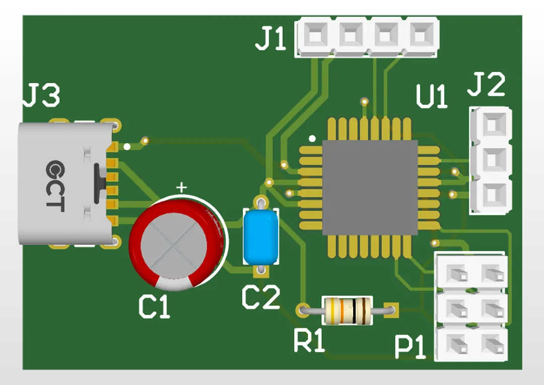
Room Temperature Display
For my first-ever PCB project, I wanted to create something simple but with some challenges. After some thought, I decided to design a room temperature display. The project should not require Wi-Fi, to keep things simple, but it would still utilize a microcontroller.
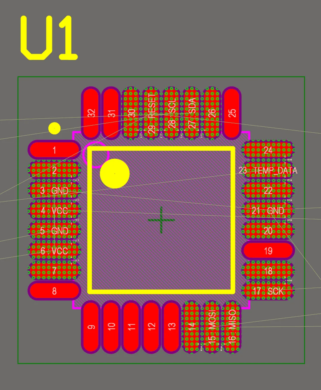
After researching, I chose the Atmega MCU because it had all the pins I needed and was easy to solder. The datasheet provided all the necessary information about the microcontroller, including pin assignments, peripheral connections, and power requirements. Since the display and temperature sensor I already had at home each had pre-soldered pins, I decided to use pin headers for easy connection.
Schematic Design
The next step was designing the schematic. I began by selecting the appropriate components and organizing them based on how I planned to use them.
Flashing the MCU
One important consideration was how to flash the software onto the MCU. The simplest solution I found was to use SPI. SPI (Serial Peripheral Interface) is a standard communication protocol that allows easy communication between devices. I decided to add six pins to my design to facilitate SPI communication and load the bootloader.
Adding Components and Connections
After finalizing my component choices, I began adding them to the schematic. Altium allows you to create custom components if they are not already available or if specific footprints and 3D models are not provided. Alternatively, you can use components directly from manufacturers, which often include pre-defined footprints and 3D models.
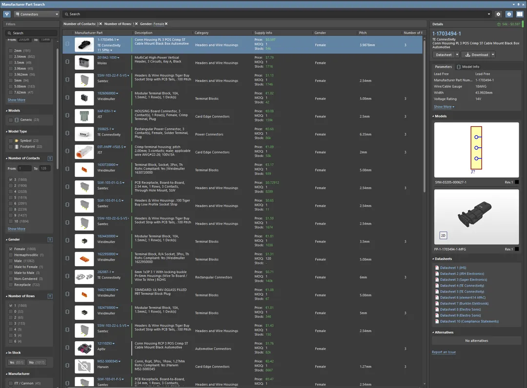
The Manufacturer Part Search in Altium is particularly useful for finding components. The parts come with datasheets, footprints, and sometimes 3D models. This search tool aggregates data from various suppliers via OctoPart, making it easier to compare prices and availability.
Once I found the necessary components, I placed them in the schematic using a right-click to “Place” or drag-and-drop them. I ensured to organize everything clearly, following a left-to-right workflow for better readability. Using the shortcut “CTRL W,” I connected the components using wires, which formed nets. A net represents a specific connection like GND, VCC, or SCL.
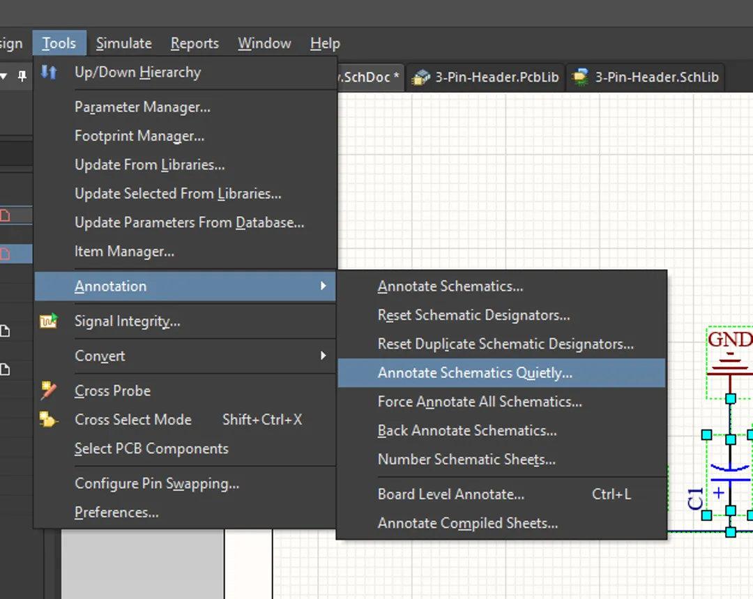
Working with Designators and Nets
To keep the schematic organized, I labeled nets where necessary. While it’s not mandatory to label every net, it helps with smaller projects to maintain clarity. In larger projects, the system automatically names nets when they are not labeled.
I also made sure to properly orient the components to make the design more readable. I used the space bar to rotate components if necessary. Altium also allows me to manually set designators or auto-number them sequentially (R1, R2, R3, etc.).
For complex components, multiple schematic sheets might be required. If the schematic becomes too cluttered, you can move parts to another sheet. To connect nets between different sheets, you can use Ports or Harnesses, which are helpful for more complex connections like USB or HDMI.

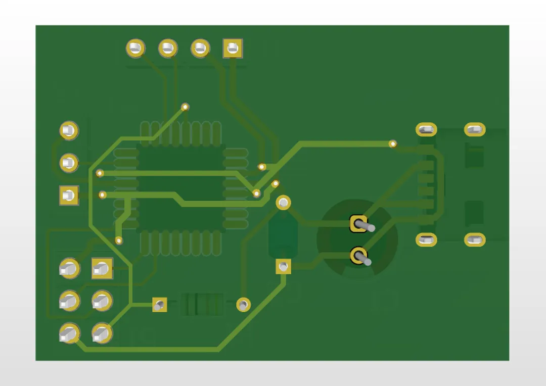
PCB Design
Once the schematic was ready, I moved on to the PCB layout.
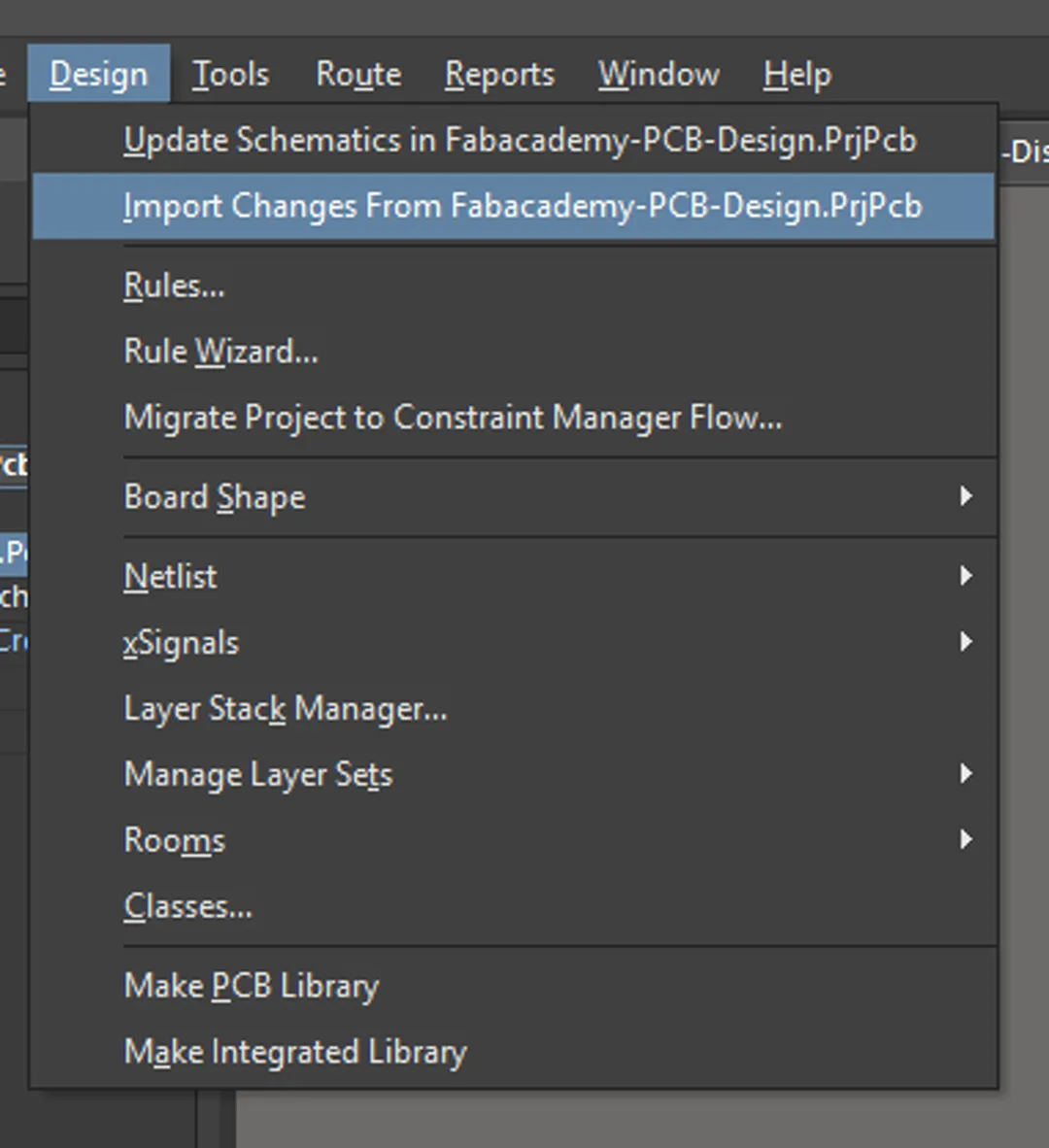
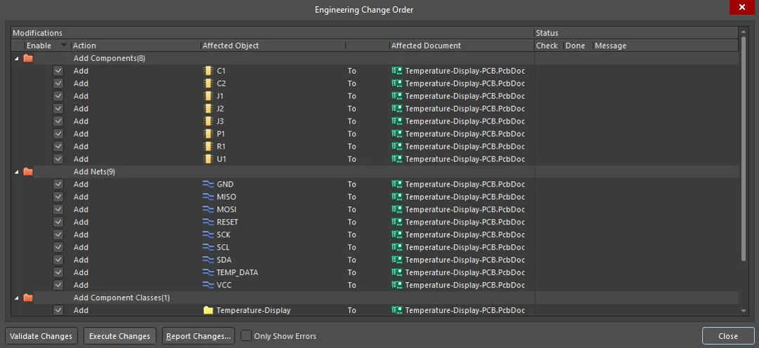
Importing Changes and Defining the PCB
To bring the components into the PCB layout, I selected “Design > Import Changes from ProjectName.PrjPcb.” If there are any changes in the schematic later, they can be updated in the PCB layout using “Update Schematics in ProjectName.PrjPcb.”
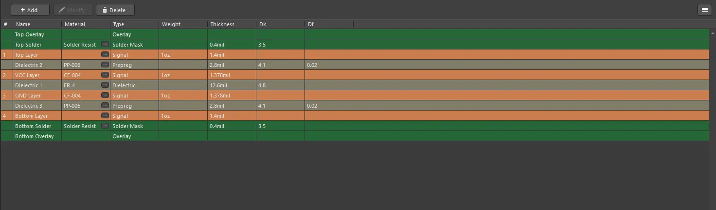
Defining the Stackup
When starting the PCB layout, the first step was to define the PCB stackup. The stackup defines the number of layers in the PCB and their structure. For professional designs, the stackup can consist of multiple layers of copper and insulating layers, but for simpler projects, it may only consist of two or maybe even just a single layer. The PCB’s design can also influence the width of traces, so it’s essential to define this stackup at the beginning.
Design Rules
You can set custom design rules by pressing Design > Rules. I defined several design rules to ensure the PCB could be manufactured correctly and function properly.
Wire Thickness and Via Sizes
Wire Thickness: Defining the thickness of the wires ensures that they can carry the necessary current without overheating. Different nets may require different wire thicknesses, especially for power lines versus signal lines.
Via Sizes: Vias (small holes that connect layers of the PCB) need to be correctly sized. For example, I set the via diameter to 10-12 mils.
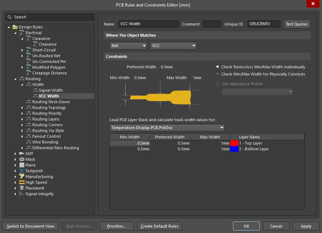
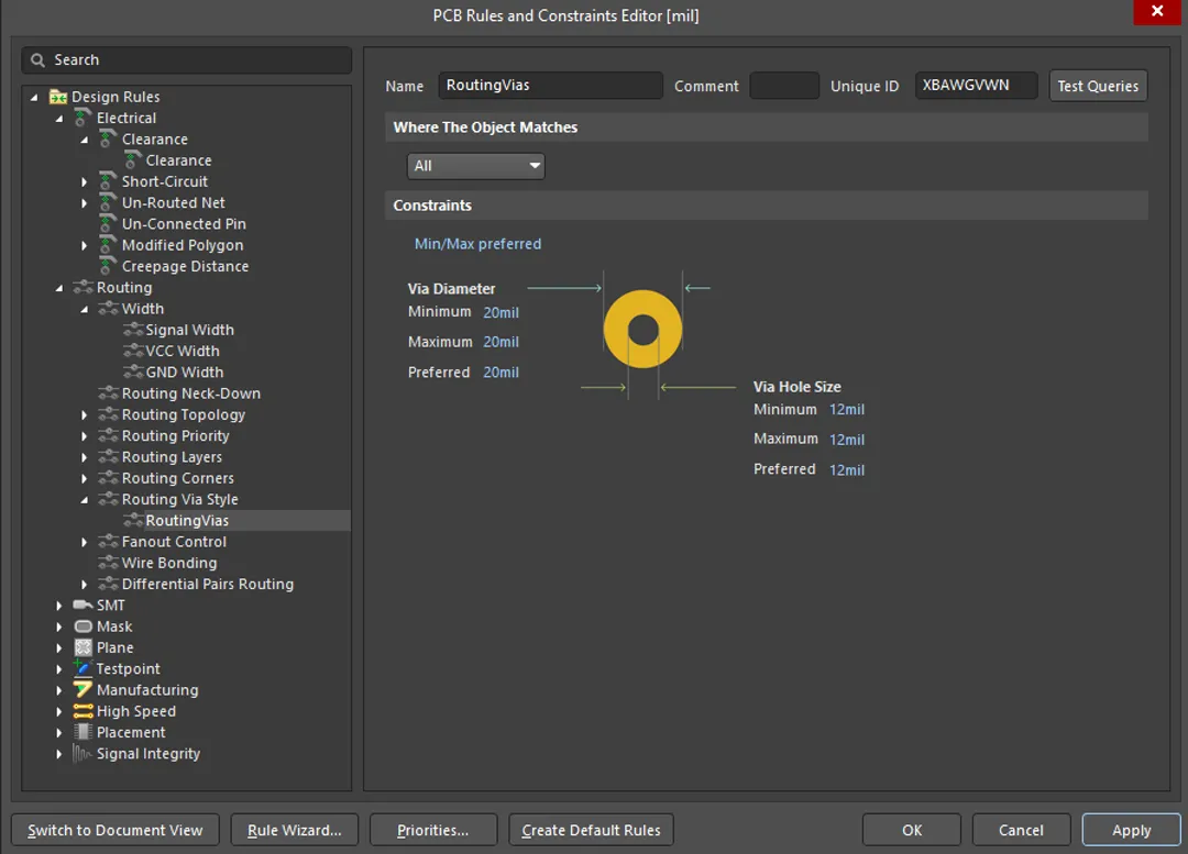
Clearance
Clearance: Ensuring that there is enough space between different components (like wires and vias) prevents short circuits and manufacturing issues.
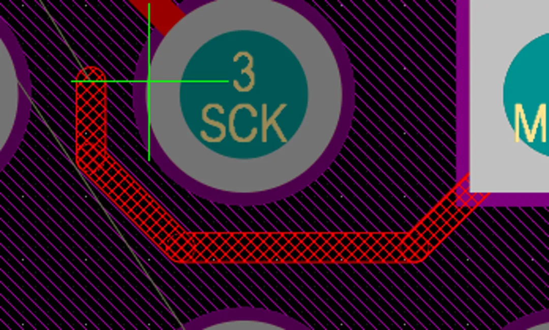
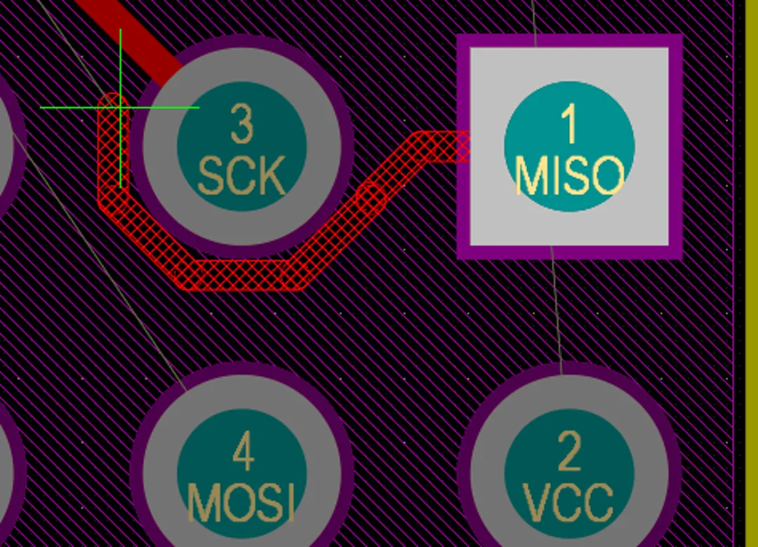
Routing and Review
After defining the design rules, I started routing the PCB. I began with the largest components that have the most pins and the most rigid placement constraints. Components that share nets should be placed closer together to save space. In cases where crossing wires is unavoidable, vias can be used to connect different layers.
Types of Vias
There are different types of vias used for layer connections:
Through-Hole Vias
These connect the top and bottom layers of the PCB and are the most commonly used type.
Buried Vias
These are not visible from the top layer, as they start from one inner layer and end in another.
Blind Vias
Similar to buried vias but start from the top or bottom layer and end somewhere in between.
Review
Once all the connections were made and the routing was complete, I conducted a final review of the PCB. Altium automatically checks for design rule violations and shows errors with green X’s in the viewport. If the design is ready, it can be sent for manufacturing.
I’ll keep you updated once I finish my course and proceed with manufacturing and ordering a PCB!
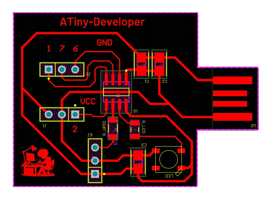
Creating a Dev Board
After learning the basics, I now feel comfortable creating a development board that lets you use the chip’s GPIOs just like you would on any other dev board. To build it, I only used parts from the Fab Inventory, of course. This ensures that every FabLab can reassemble my design.
For the design process, I started again in Altium Designer and added the main component of the board: the MCU. In the MCU’s datasheet, you can find all the details about its GPIOs and what it might need.
Similar to my practice project above, I also needed to add a few capacitors to make sure the chip doesn’t reset or glitch when energy spikes occur on the supply lines.
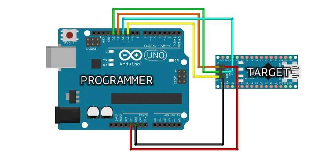
To push the code to the board, I needed an interface. The ATtiny uses UPDI for that. This works similarly to SPI but uses only three wires: GND, VCC, and the UPDI pin.
For it to work reliably, the UPDI pin needs a 4.7 kΩ resistor in series with its connection. This resistor acts as a weak pull-up / current-limiting element that prevents the programmer and the target microcontroller from driving the line against each other or causing false bit transitions when the line is idle, which stabilizes the bidirectional communication on this single wire.
Last but not least, I wanted to add an RGB LED to make rapid prototyping easier by providing fast visual feedback.
To run the LED, I also had to add a 330 Ω resistor to its data net to limit current and protect both the MCU’s output and the LED.
And of course, I also added some pin headers for the GPIOs.
After taking all that into consideration, I looked up the parts in the inventory and added them via the Part Manufacturing Page in Altium, as mentioned above. The rest of the PCB design was pretty straightforward, especially after the learnings from above.
For the power, I recreated a USB-A footprint using an external footprint from EasyEDA. This one is from EasyEDA and currently allows an Altium export in beta.
For me, it worked quite well. The downloaded file could simply be opened in Altium and converted into a library via the file export, which I then loaded into my dev board project.

To import external footprints or library files into Altium Designer, you can use File → Import Wizard, which guides you through the process of selecting and converting design files or library formats from other tools into Altium’s native formats.
Lastly, I also added a little graphic of that very developer in the lower-left edge. To do this, you can press Place > Graphics or P > H and then draw the boundary size of the image to import.
A standard PNG works, but as you know from image tracing / converting an image to a binary file - copper or no copper - use a simple, already binary-colored, ideally black-and-white image.
After laying out the final PCB, I added some minor details that make life easier. I numbered the GPIO ports so they can be easily identified, and I added a title to the board: “ATiny-Developer” ... since it uses an ATtiny ... you know? Anyway! Don’t look too closely at my board, since I might or might not have had a typo here... which I fixed... but it seemed to come back after a CTRL+Z.
Since I can’t add any solder masks, I went ahead and added it to the top copper layer. Of course, you can also switch it to the bottom layer or place it on an extra mechanical layer, which you can later control individually in the PCB machine’s software.
After all these considerations and tasks, we finally end up with a cute and fancy little dev board, ready to be produced next week!

Simulate a Circuit
Wokwi
Wokwi is an online microcontroller and electronics simulator that runs right in your web browser. It lets you design, build, and simulate circuits with virtual hardware such as Arduino, ESP32, STM32, sensors, displays, and more, all without needing any physical components.
You write your source code in the Wokwi code editor and the simulator compiles and runs it like real firmware on the virtual board, so you can test behavior before using real hardware.
Setting up Wokwi
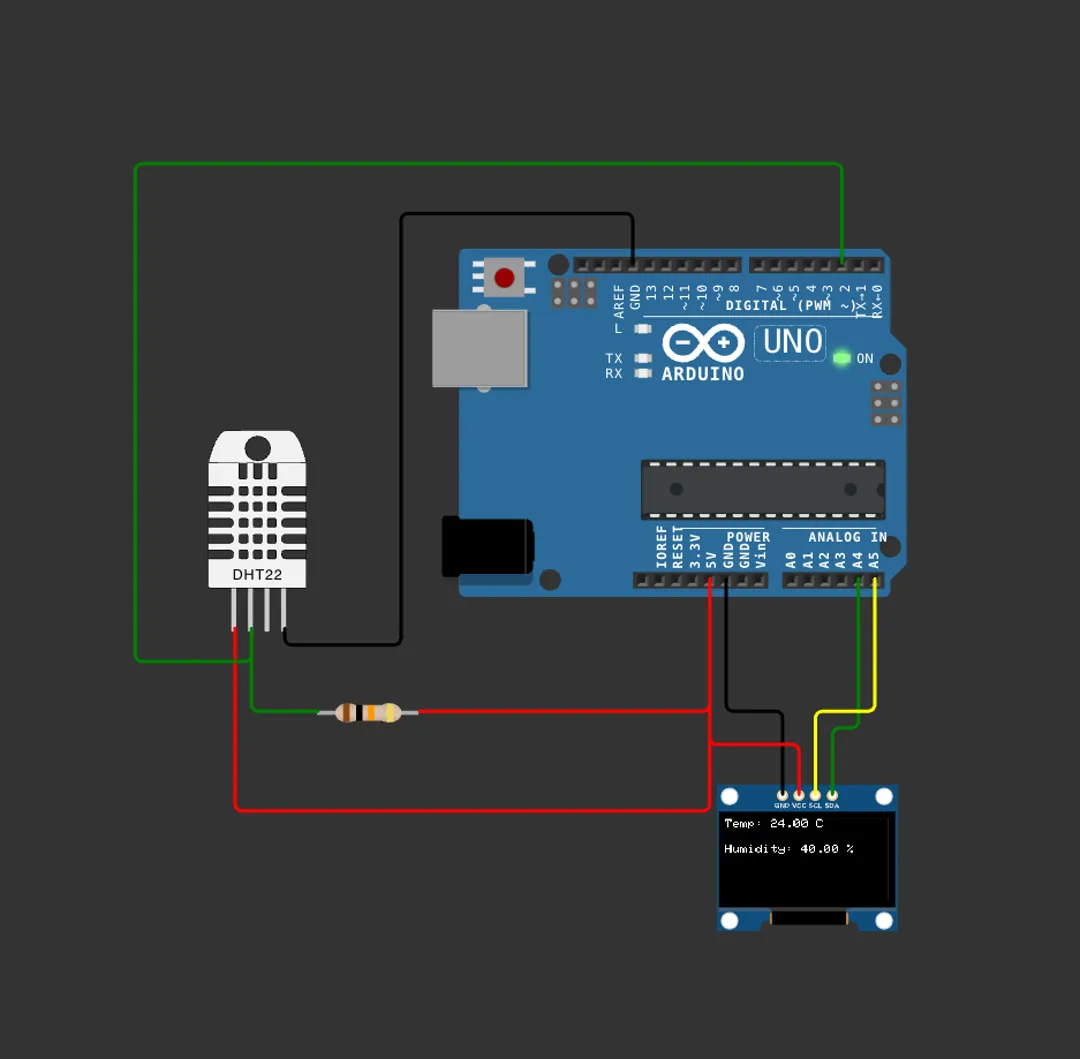
1. Create a Project: Go to the Wokwi website and start a new simulation project, for example with an Arduino UNO.
2. Add Components: On the circuit view, click the purple + button to open the component picker. Search for parts like a DHT22 sensor, OLED display, and more. Clicking a component places it into the workspace.
3. Move / Arrange Parts: Drag and drop each part to arrange them visually on the canvas. You can also rotate parts using R.
4. Connect with Wires: To connect pins, click on a pin of one component, then click the target pin on another component. This draws a wire between them. Advanced users can also edit the diagram.json file directly to change connections or component properties.
5. Component Details / Documentation: Clicking the little ? icon on a part brings up documentation for that part so you can check pinouts and expected behaviour.
If your sketch uses external libraries (like DHT, Adafruit_SSD1306, etc.), you can add them via the Library Manager found above the editor. Search and add the ones you need. If a library isn’t available, you can upload the library files manually.
Simulate in Wokwi
After writing the code and adding needed libraries, click the Play button to compile and simulate. Wokwi compiles the code into firmware and simulates every instruction on the virtual device.
#include <Wire.h>
#include <Adafruit_GFX.h>
#include <Adafruit_SSD1306.h>
#include <DHT.h>

// DHT22 Setup
#define DHTPIN 2
#define DHTTYPE DHT22
DHT dht(DHTPIN, DHTTYPE);

// OLED Setup
#define SCREEN_WIDTH 128
#define SCREEN_HEIGHT 64
#define OLED_RESET    -1   // not connected
Adafruit_SSD1306 display(SCREEN_WIDTH, SCREEN_HEIGHT, &Wire, OLED_RESET);

void setup() {
  Serial.begin(9600);
  dht.begin();

  // Display setup
if (!display.begin(SSD1306_SWITCHCAPVCC, 0x3C)) {  // Address 0x3C
    Serial.println(F("OLED not initialized!"));
    while (true);
  }

  display.clearDisplay();
  display.setTextSize(1);
  display.setTextColor(SSD1306_WHITE);
  display.setCursor(0,0);
  display.println(F("Booting..."));
  display.display();
  delay(1000);
}

void loop() {
  float temp = dht.readTemperature();
  float hum  = dht.readHumidity();

  if (isnan(temp) || isnan(hum)) {
    Serial.println(F("Error Reading Values!"));
    return;
  }

  display.clearDisplay();

  display.setCursor(0, 0);
  display.print(F("Temp: "));
  display.print(temp);
  display.println(F(" C"));

  display.setCursor(0, 20);
  display.print(F("Humidity: "));
  display.print(hum);
  display.println(F(" %"));

  display.display();

  delay(2000);
}

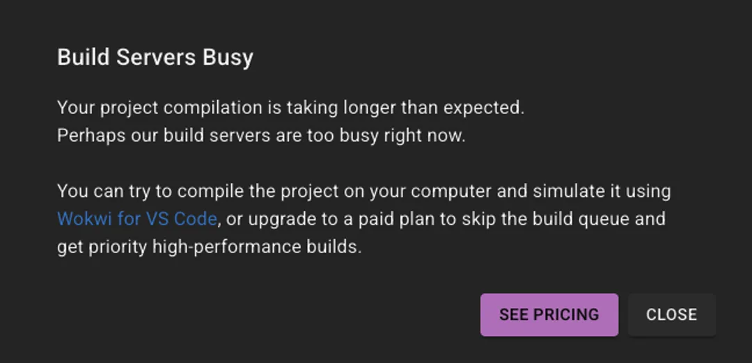
While working on the simulation, I repeatedly encountered an issue where compiling took too long and eventually failed with a message about insufficient server resources. Because Wokwi runs in the cloud, the compile process relies on available shared build servers. When server resources are limited, projects can get stuck waiting for builds. This slowed down the workflow significantly.
I observed that after a few retries, the code would eventually compile and run correctly, but the delay cost a lot of time. According to Wokwi’s pricing info, a paid subscription can speed up builds and provide more reliable resources which would likely avoid these long compilation waits.