For this week's electronics production assignment, I wanted to design and mill a PCB that would be meaningful for my final project: a wearable pomodoro timer. The idea is a small watch-sized device that uses haptic and visual feedback to mark time intervals and be used as a focus timer.
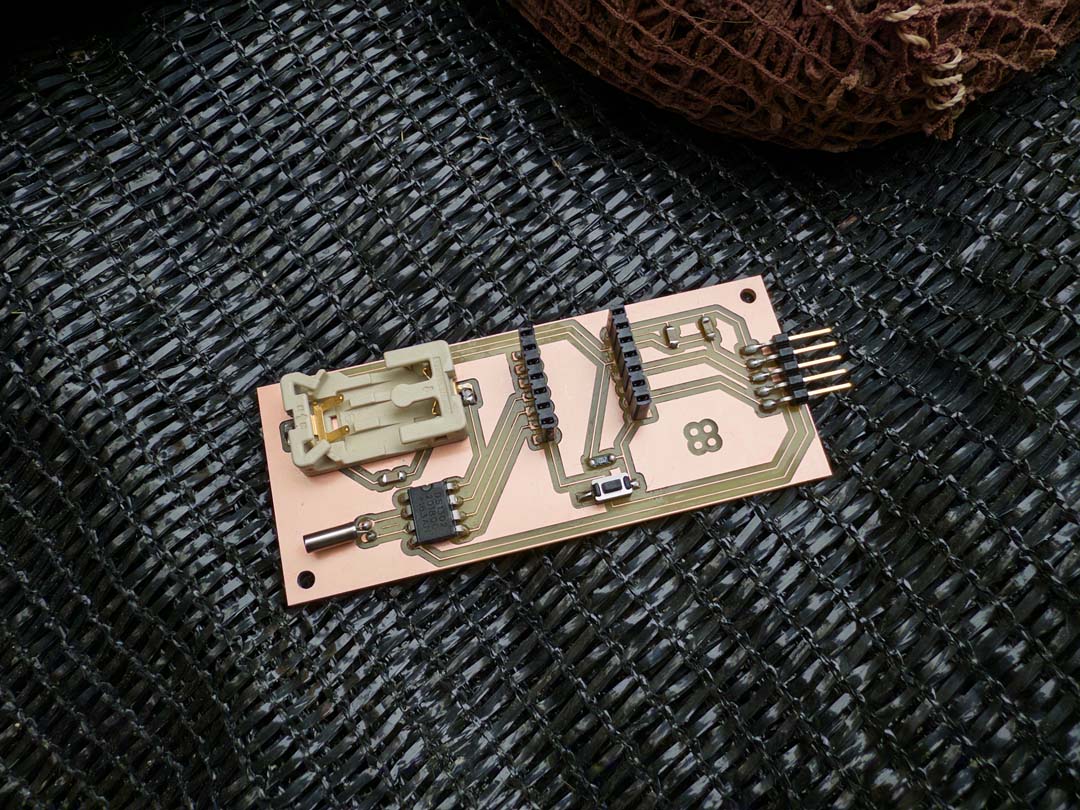
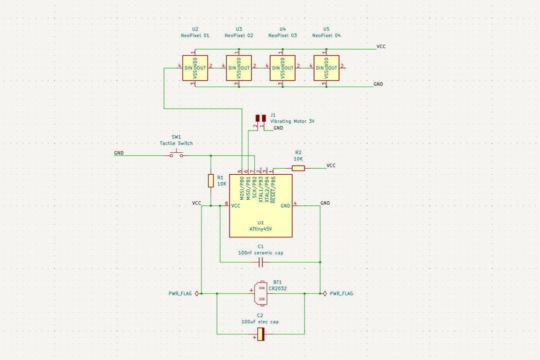
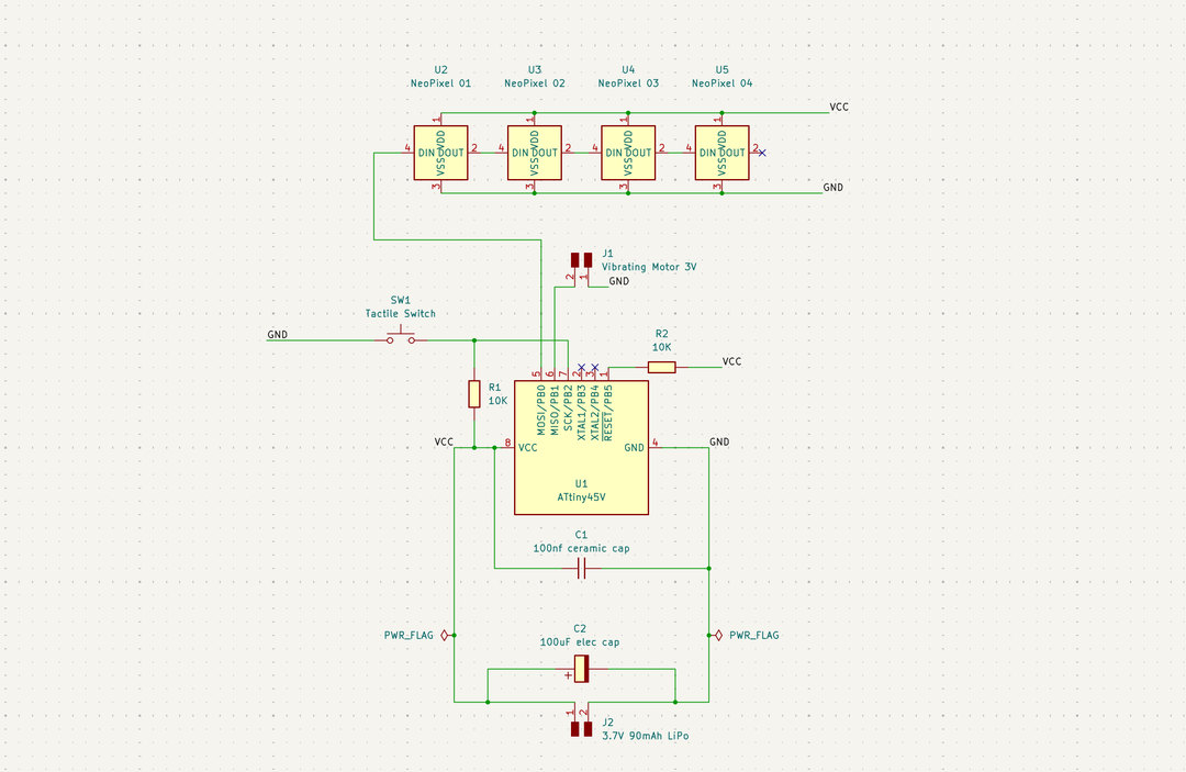
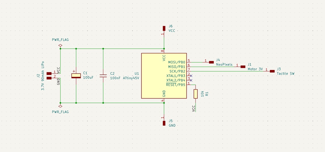
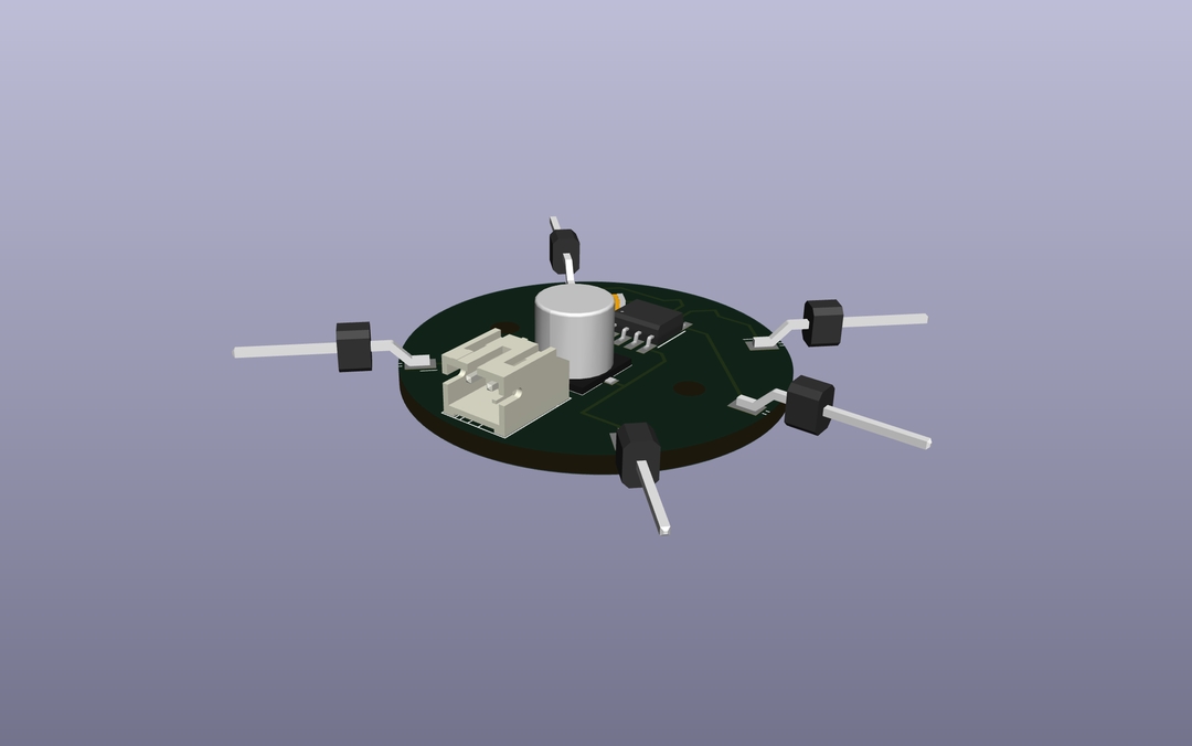
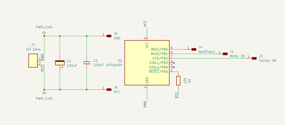
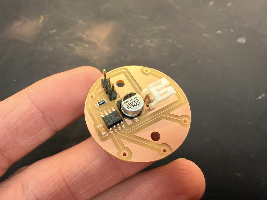
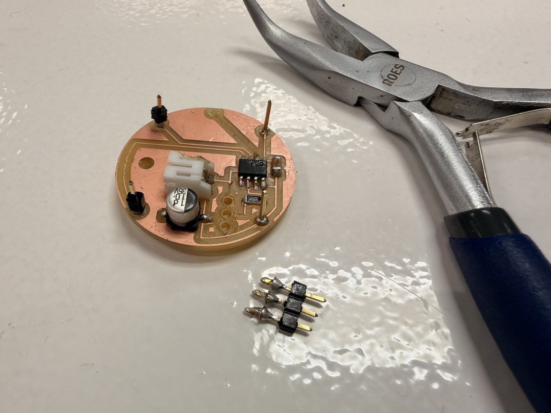
The components I knew I wanted from the start were four 5050 NeoPixels (visual feedback to show time remaining), a 10mm flat 3V vibration motor (haptic buzz at the end of an interval), and a tactile button to start and stop the timer. The first version of the design used a CR2032 coin cell for power and an ATtiny45 microcontroller. Both were swapped out later as the design evolved.
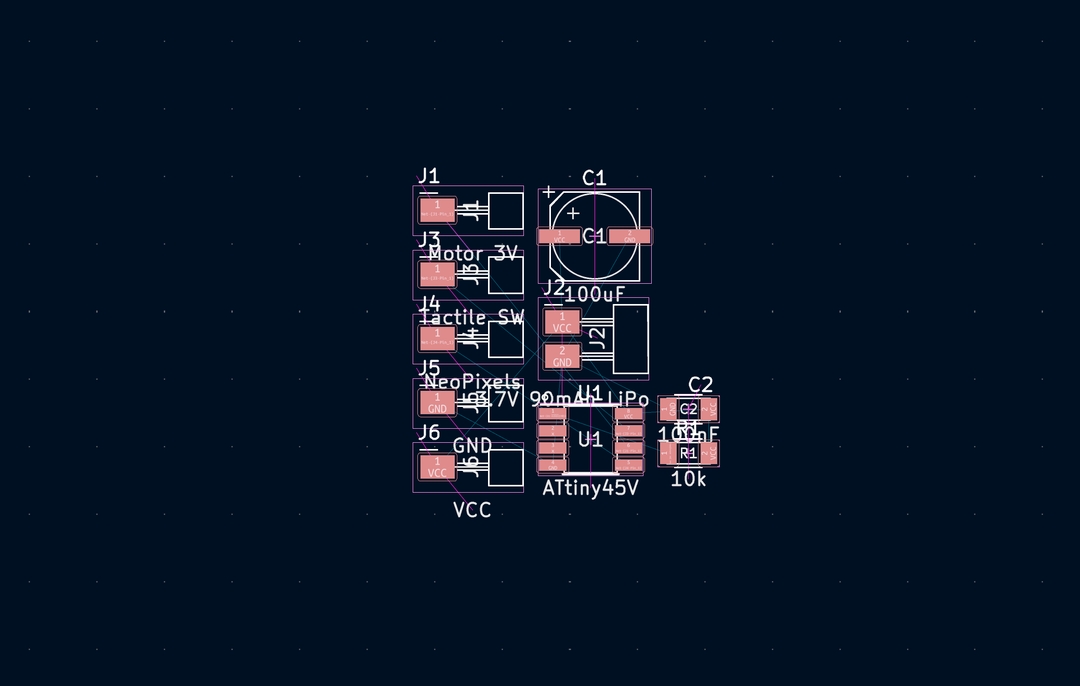
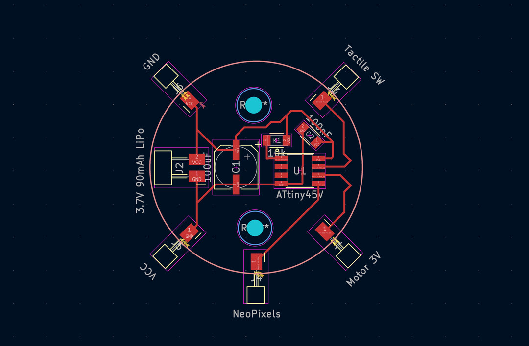
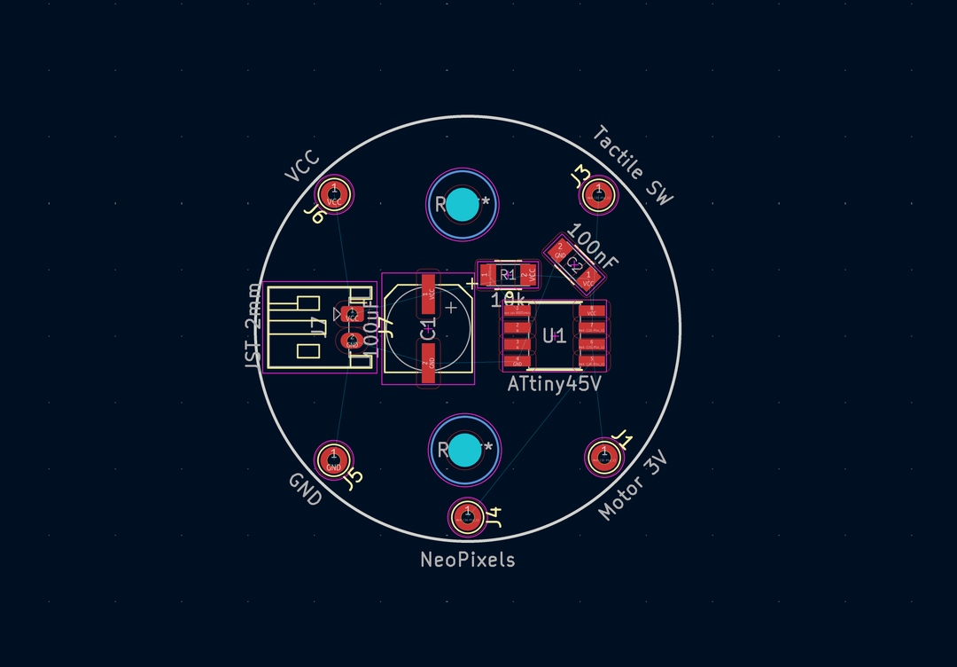
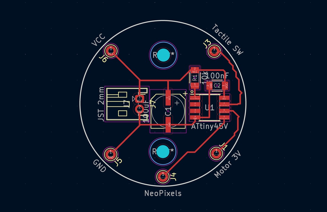
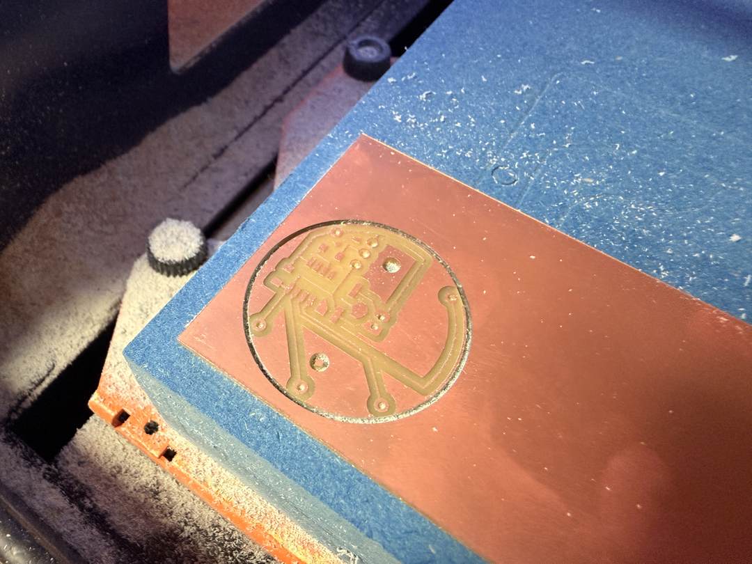
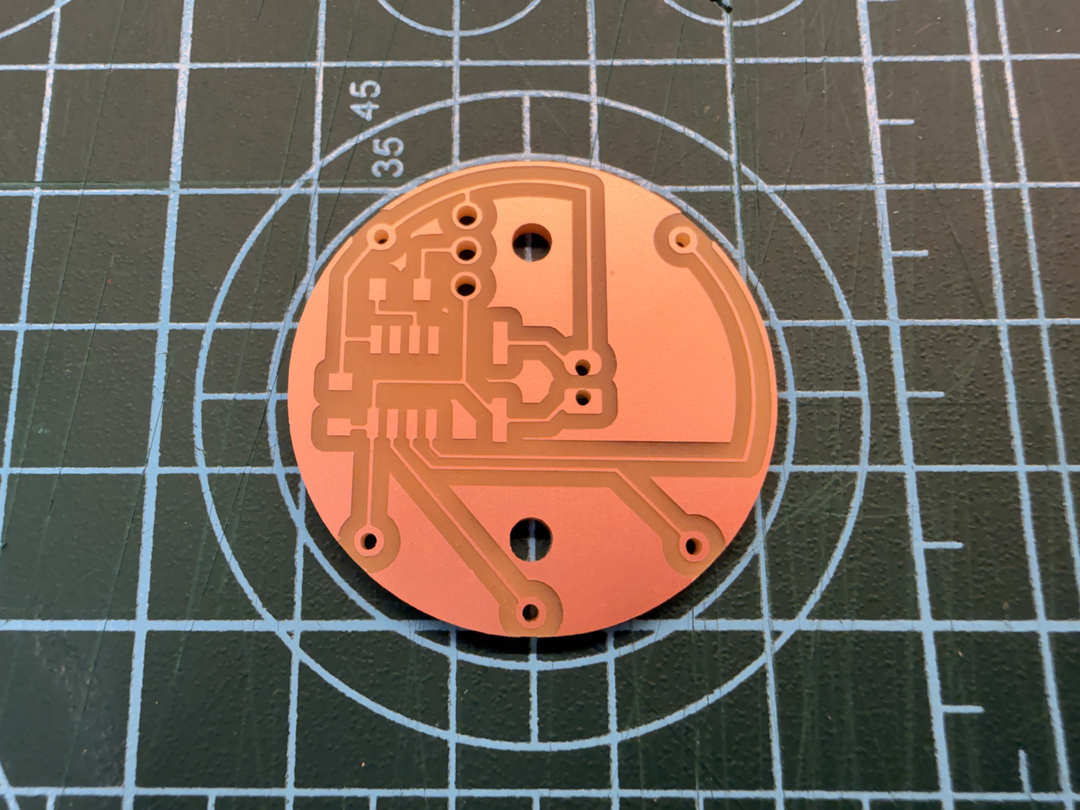
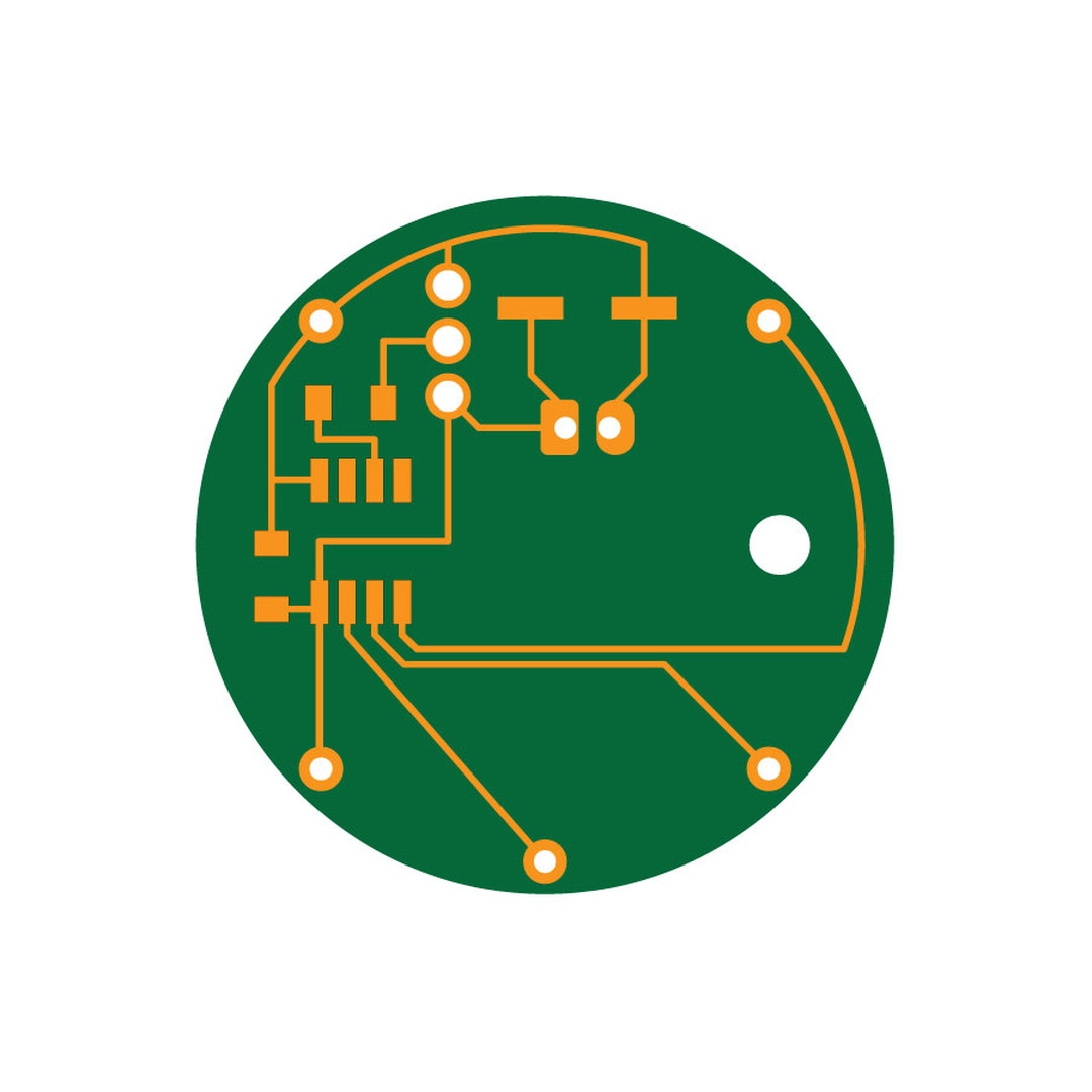
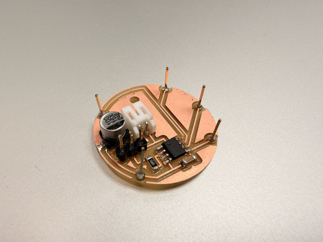
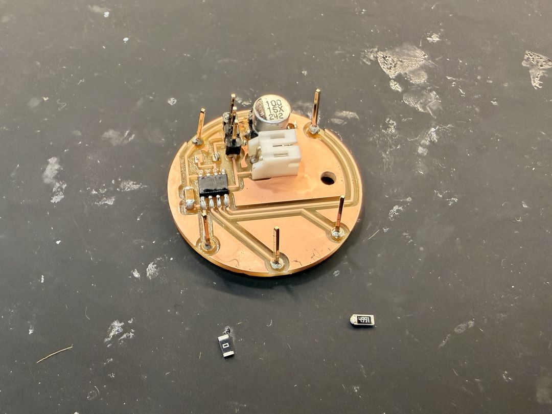
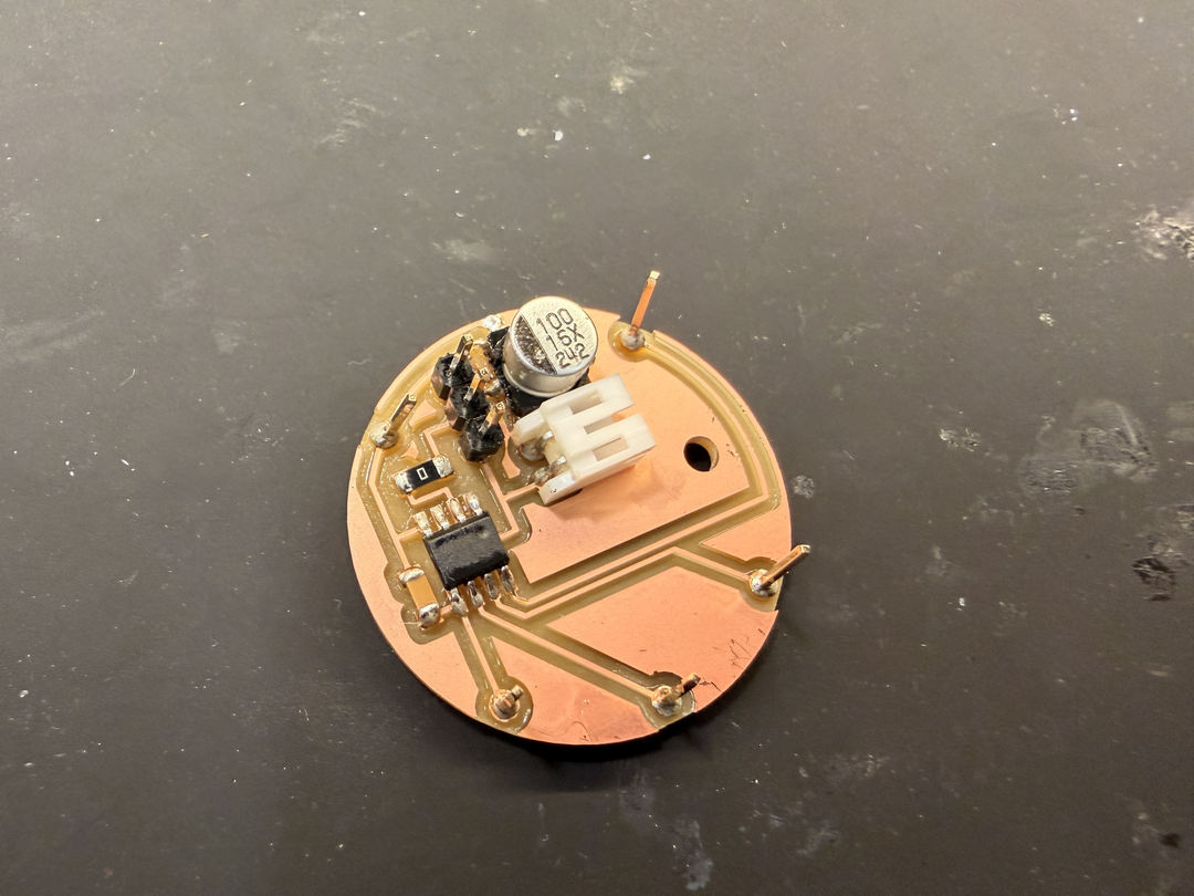
I started with a larger board to get the components and schematic right before committing to the tight constraints of a watch form factor.
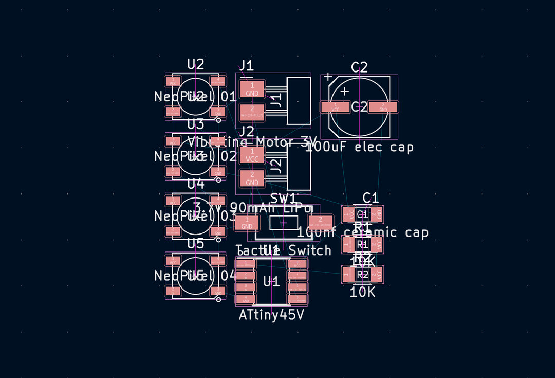
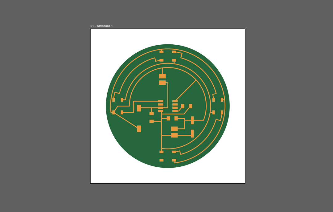
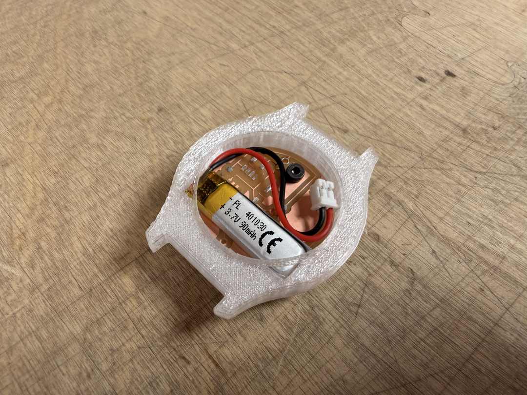
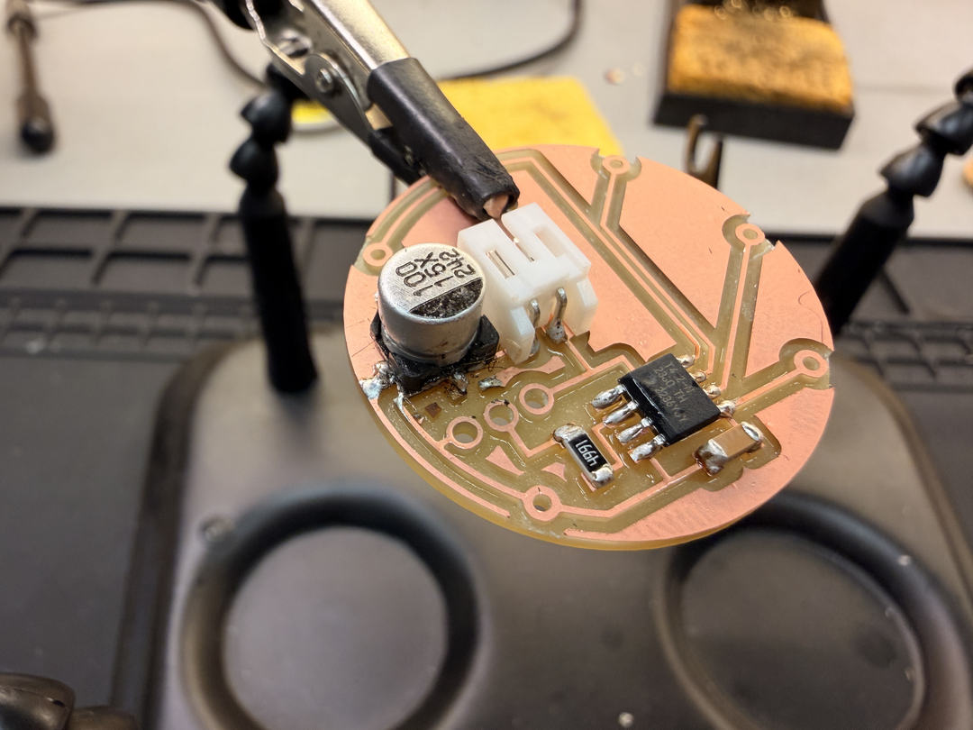
The CR2032 turned out to be a poor fit for this circuit. It's rated 3V at around 225 mAh, but four NeoPixels at full brightness can draw up to 240 mA on their own. The cell sags immediately and the usable runtime would be measured in minutes rather than hours. I switched to a 3.7V 90 mAh LiPo, which gives roughly ten times the usable capacity in this circuit and also drives the motor a little harder at 3.7V than it would at 3V. To keep the design simple for a weekly assignment I deliberately did not include an onboard charging circuit. The LiPo unplugs from the JST-PH connector and is charged externally.
KiCad project file of the first "larger" pomodoro timer test board
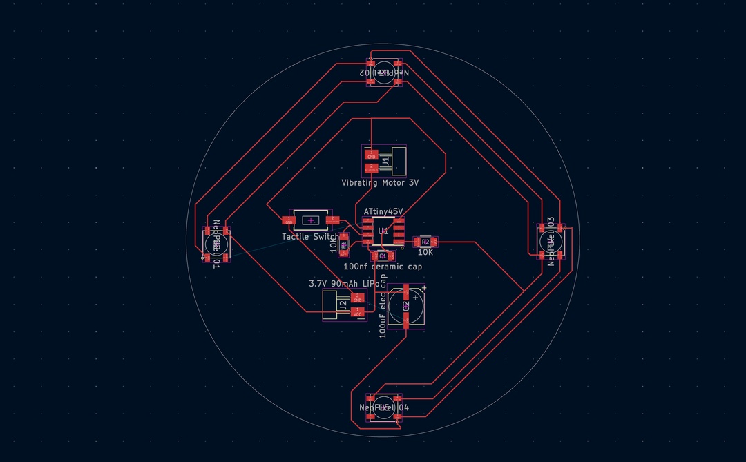
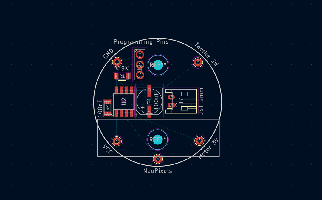
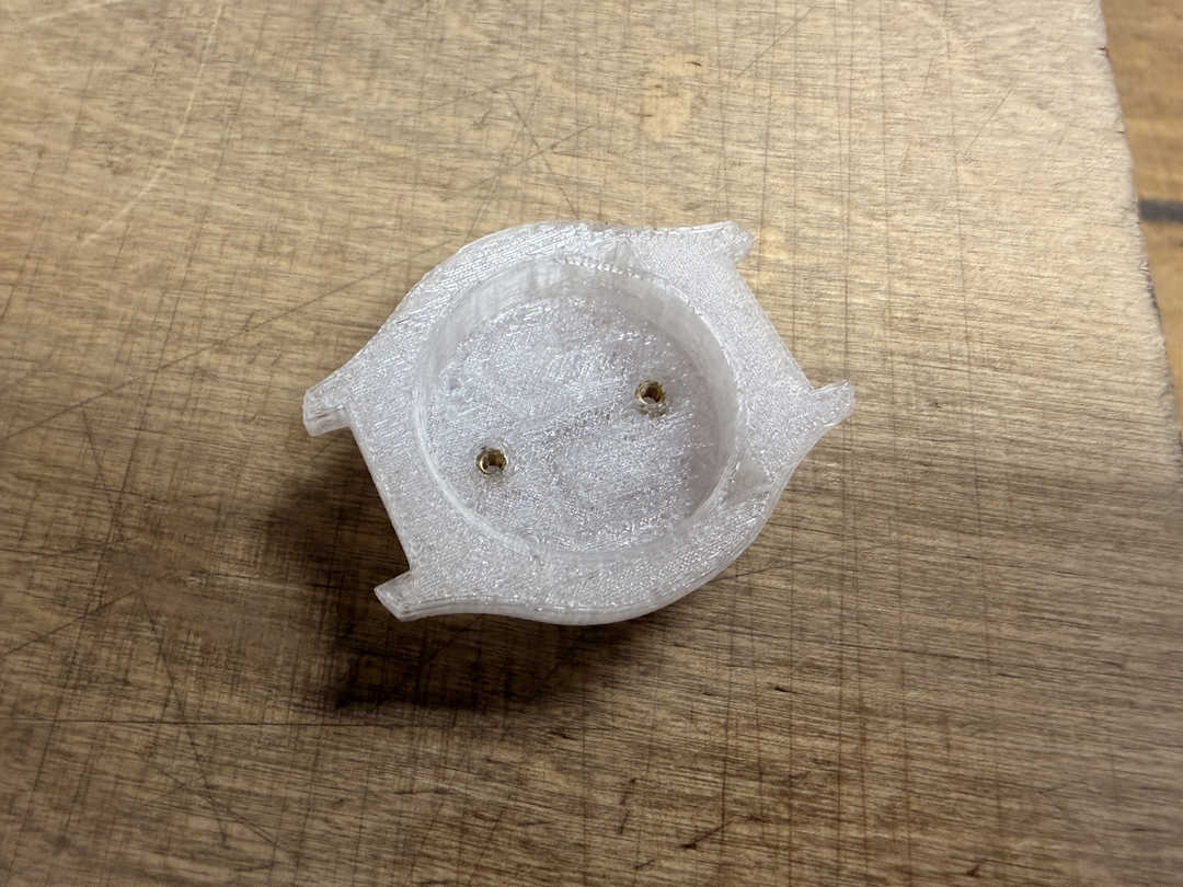
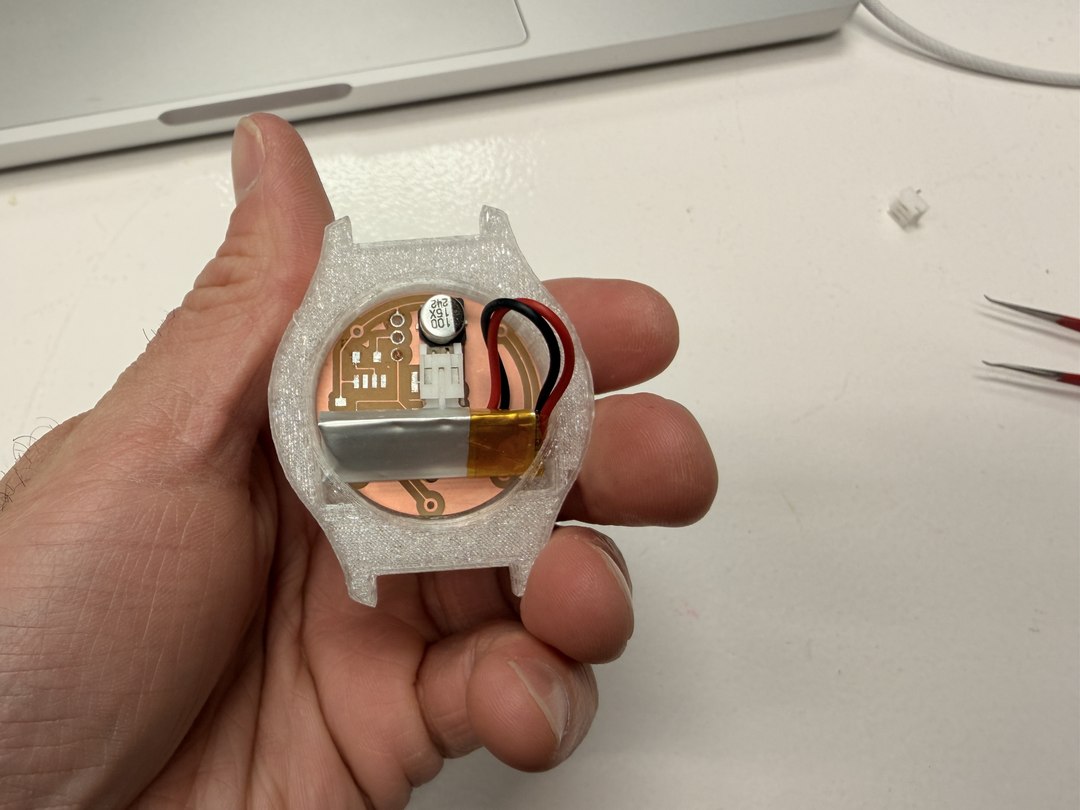
Once the schematic was stable, I decided to redesign the board in a watch form factor. The idea was to have different layers of components embedded into a 3D print, all connecting back to the main board at the bottom of the watch body by running copper wire down "via" channels in the 3D print. Above the main board, layers of the 3D printed watch body would contain: a vibrating motor, NeoPixels, and a button (with a 10k pull-up resistor) or pressure sensor.
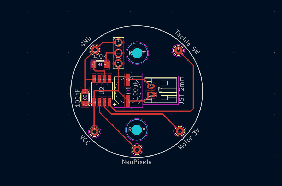
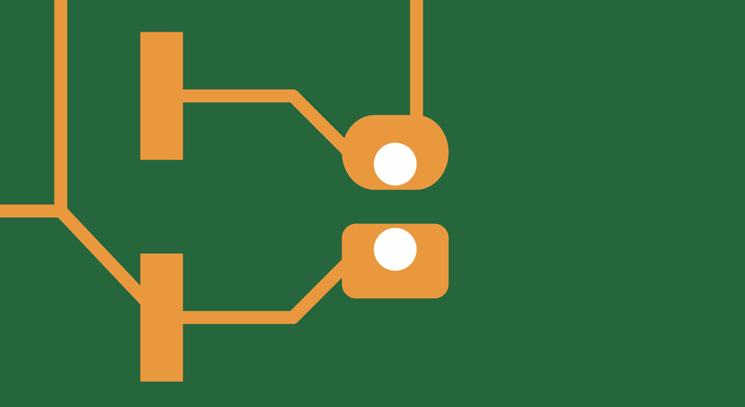
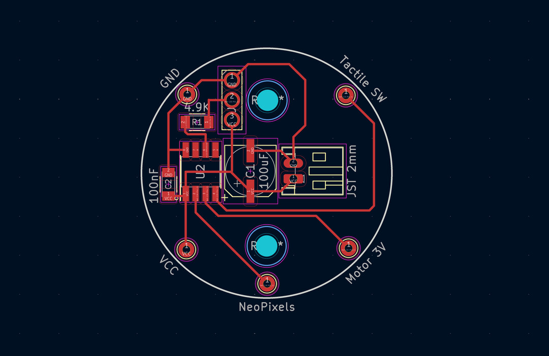
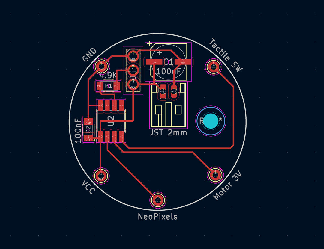
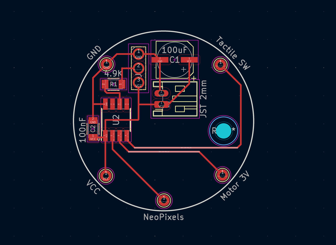
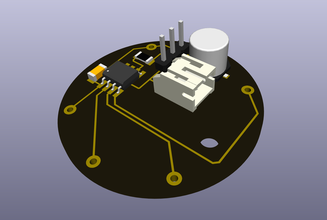
The four NeoPixels chain through their DIN/DOUT pins. The data line from PA6 connects only to the first pixel's DIN, and each pixel reads the first 24 bits of colour data, sets its own colour, then forwards the rest downstream via DOUT. VCC and GND are wired to all four pixels in parallel rather than chained.
| Qty | Component | Value / spec |
|---|---|---|
| 1 | Microcontroller | ATtiny412 (SOIC-8) |
| 4 | NeoPixel | 5050 |
| 1 | Vibration motor | 10 mm flat, 3 V |
| 1 | LiPo battery | 3.7 V, 90 mAh |
| 1 | Battery connector | JST-PH 2-pin |
| 1 | Tactile button | SMD |
| 1 | Capacitor (bulk) | 100 µF electrolytic |
| 1 | Capacitor (decoupling) | 100 nF ceramic |
| 1 | Resistor (button pull-up) | 10 kΩ |
| 1 | Resistor (UPDI series) | 4.7 kΩ |
| 1 | Programming header | 3-pin THT (VCC / UPDI / GND) |
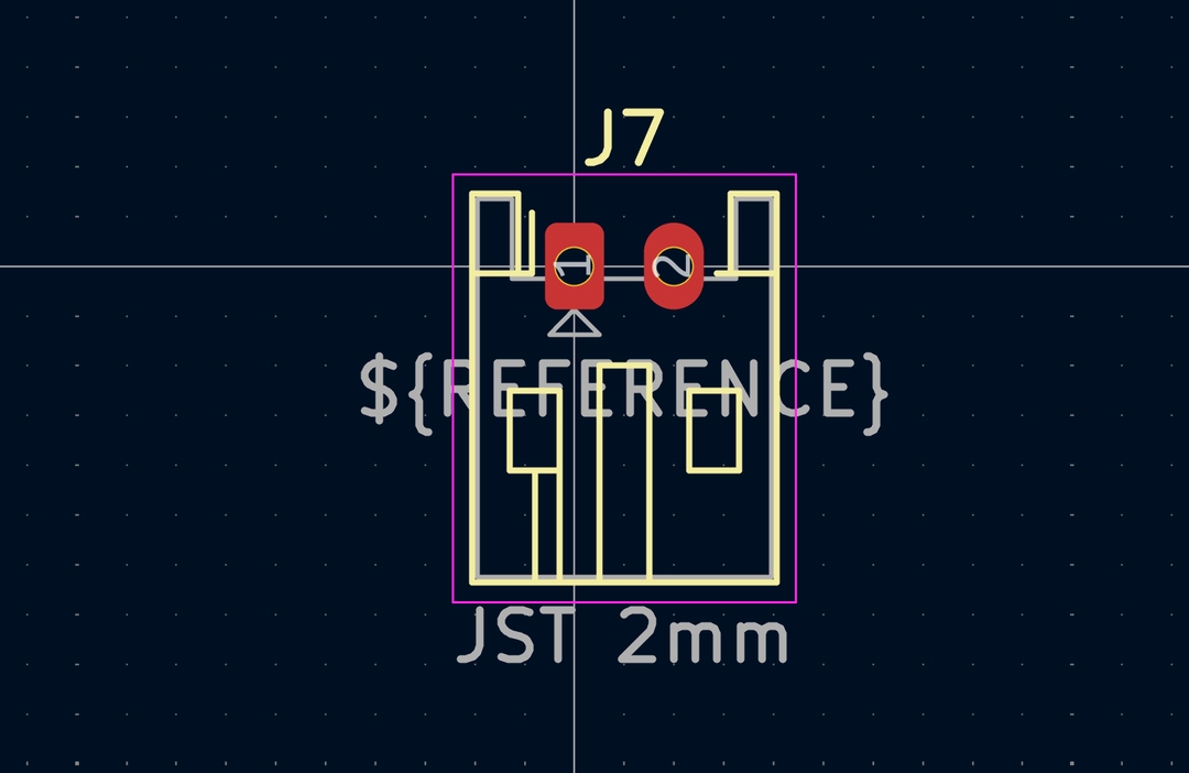
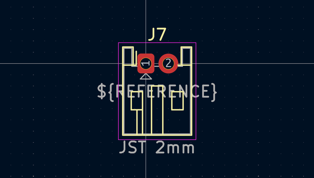
I needed to add a JST connector for the LiPo battery. I looked up the datasheet to get the correct footprint dimensions and hole sizes, then made adjustments in KiCad.
KiCad project file of v1 of the watch pomodoro timer
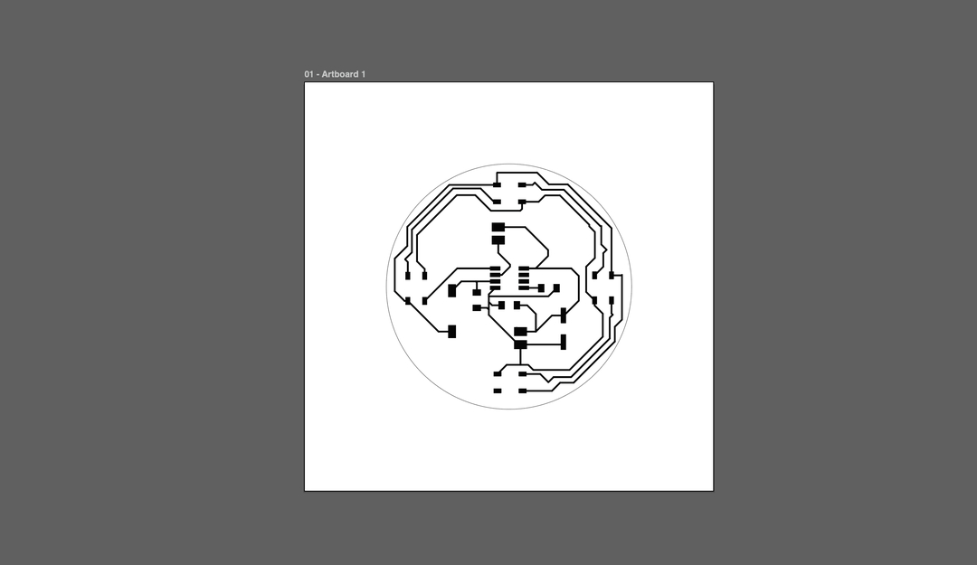
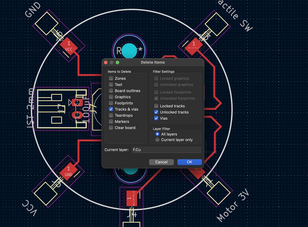
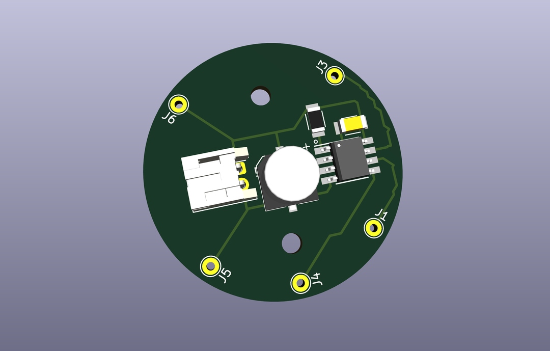
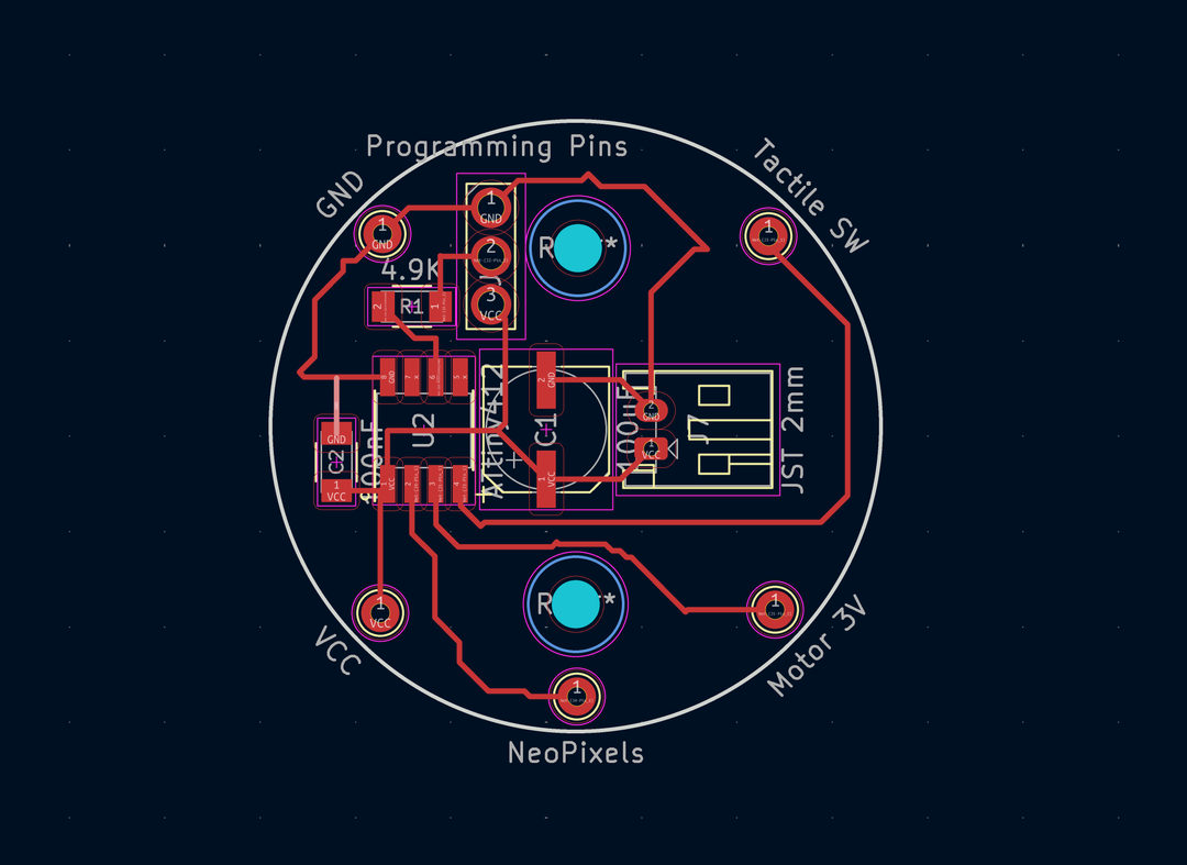
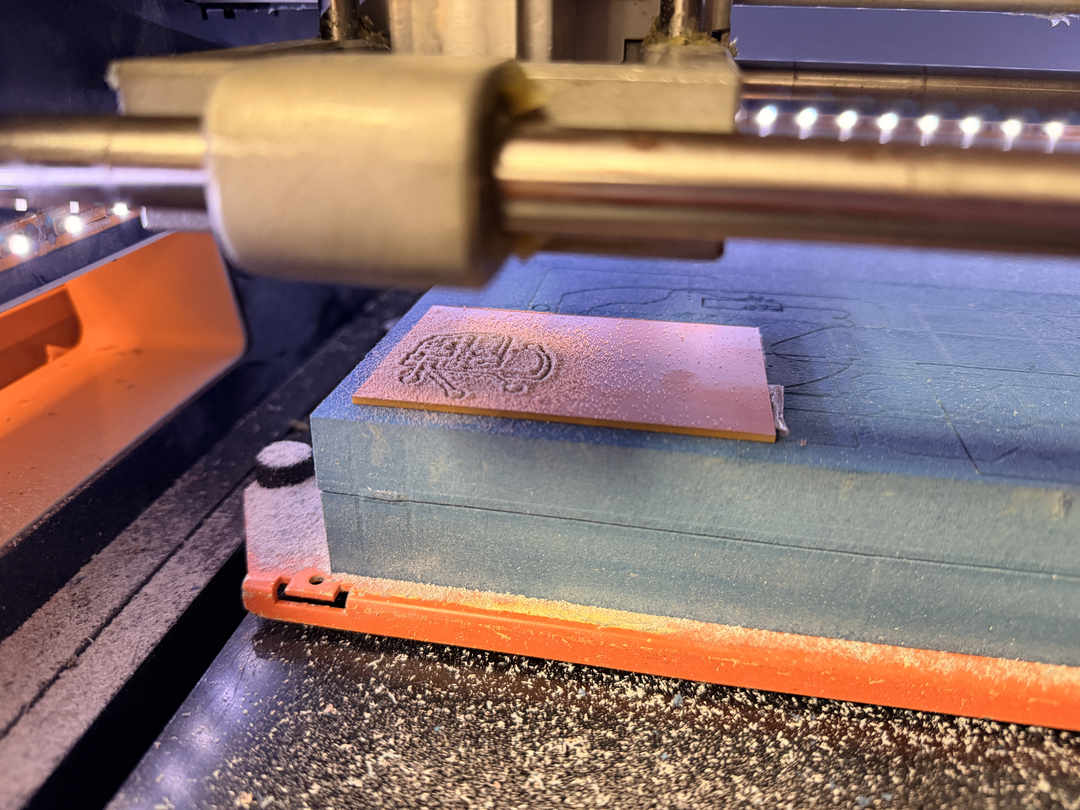
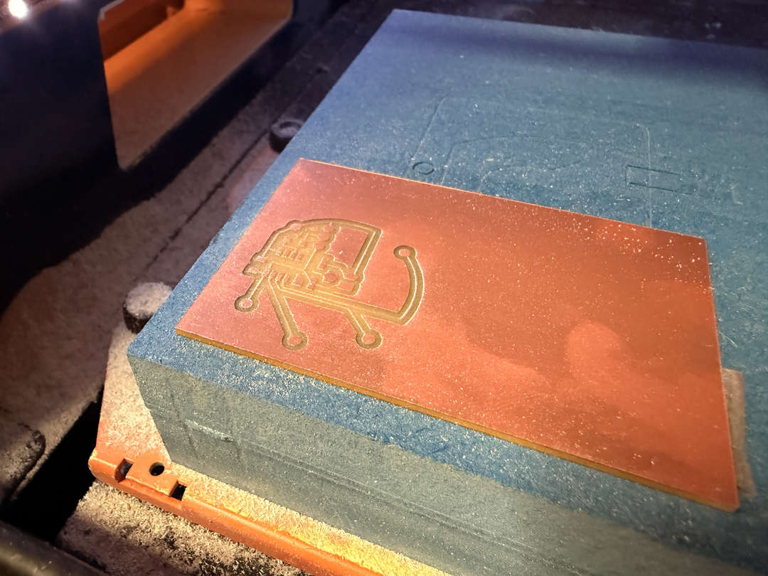
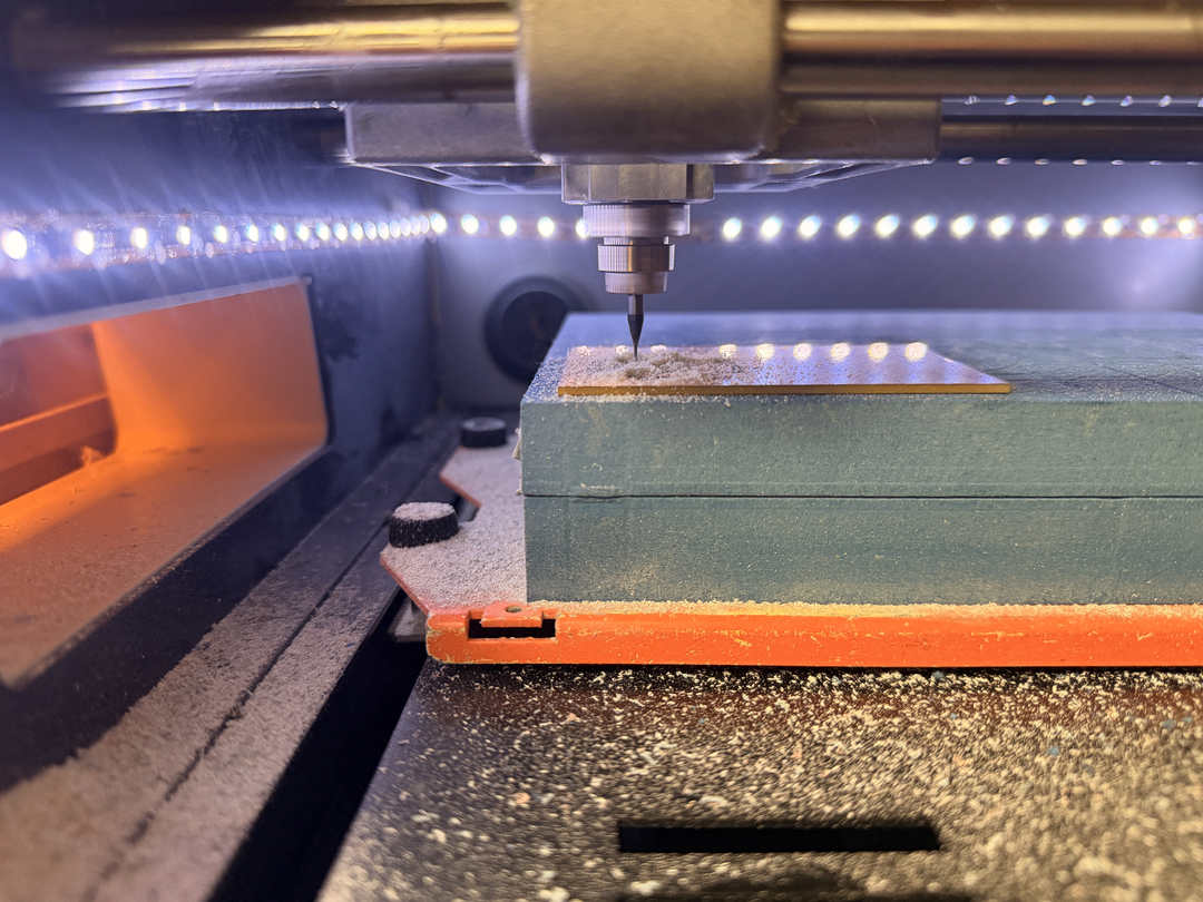
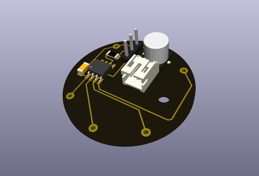
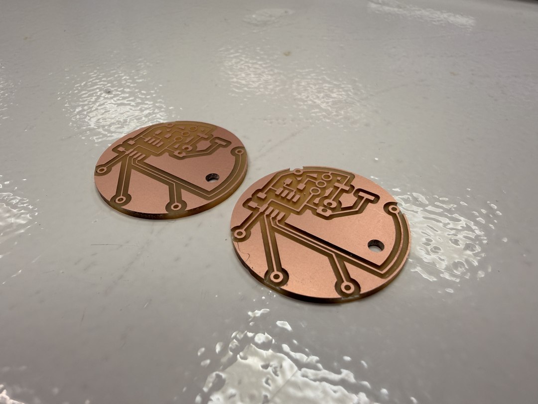
I made a second pass at the PCB design to fix routing issues, better position the battery connector, and tighten the overall layout for the milling machine constraints (minimum trace width 0.3mm and clearance of 0.4mm).
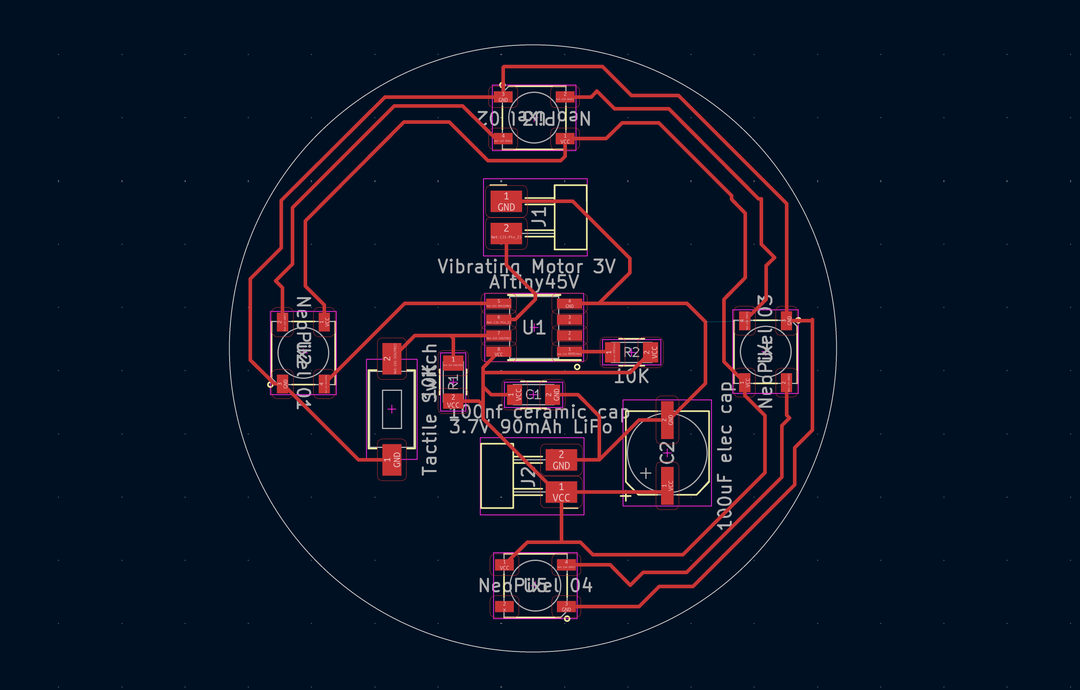
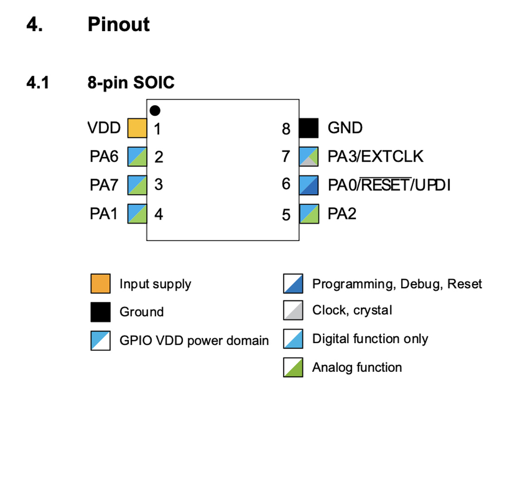
I also switched the microcontroller from the ATtiny45 to the ATtiny412. The reason was the programming protocol: the 412 is part of Microchip's tinyAVR 1-series and uses UPDI, a single-wire programming interface. That means the programming header on the board only needs three pads (VCC, UPDI, GND) instead of the six required by ISP on the ATtiny45 family.
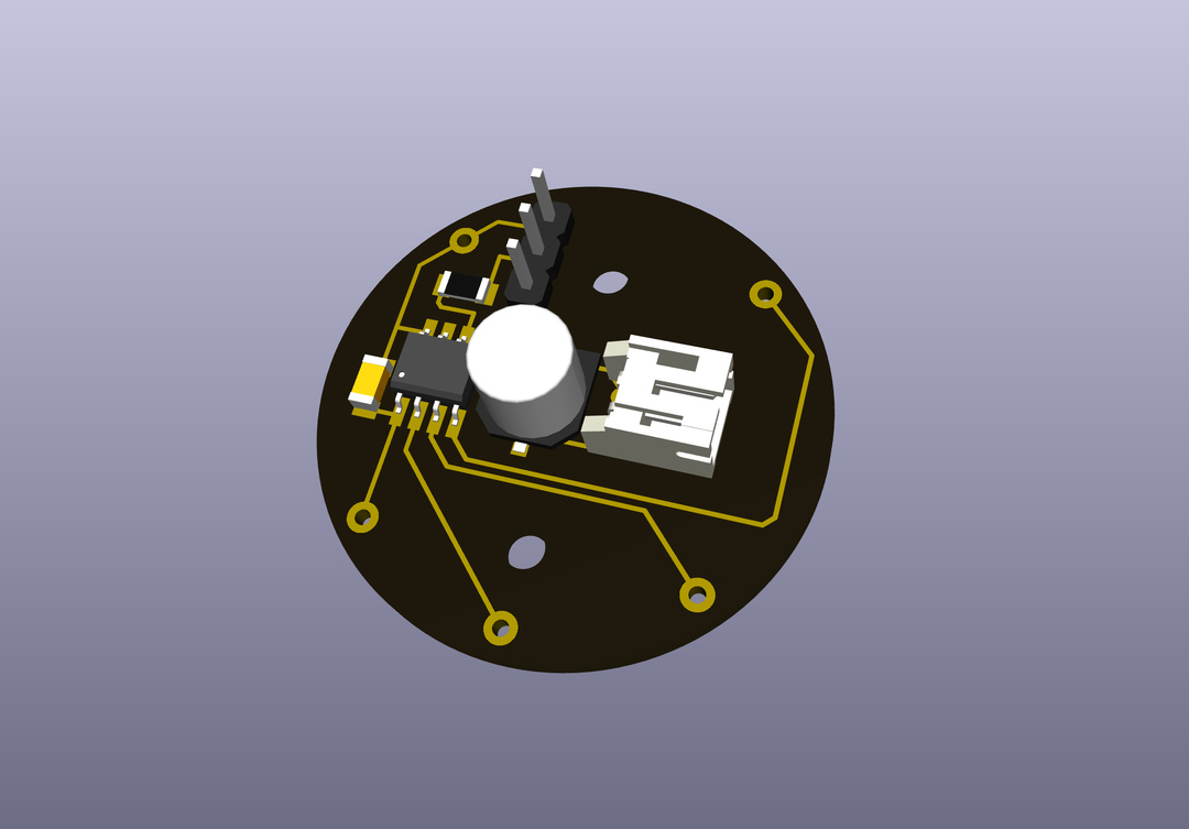
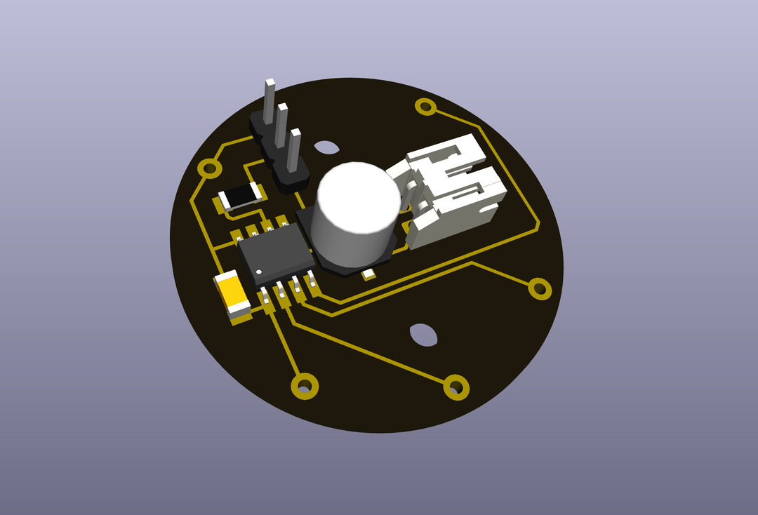
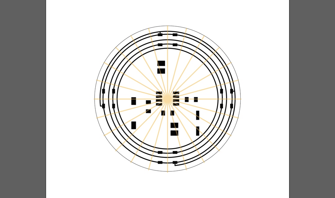
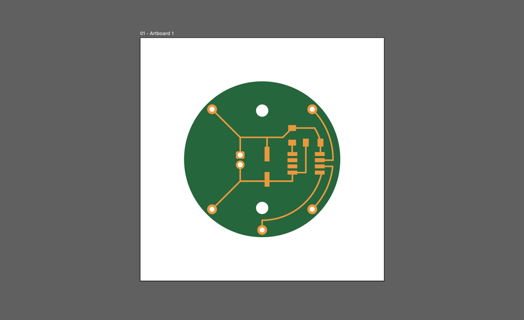
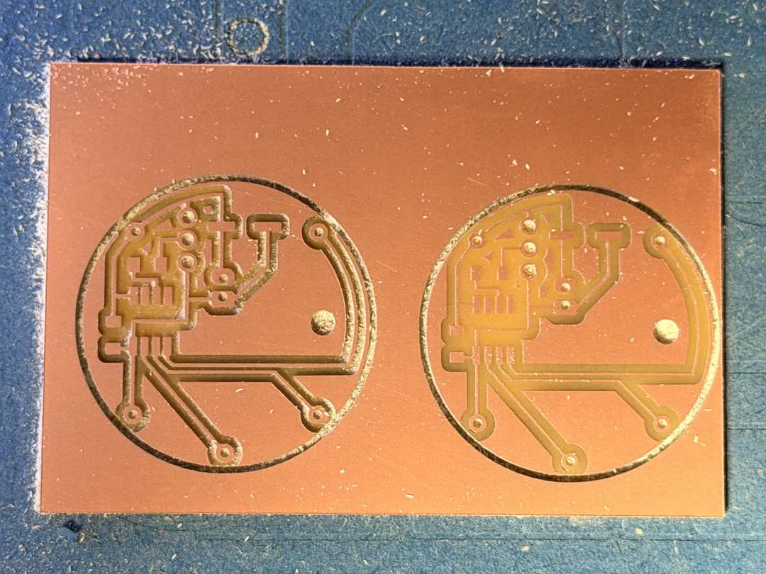
Before milling I needed to fix the JST pad footprint and export the traces, holes, and edge cuts as separate PNGs through the MODs project workflow.
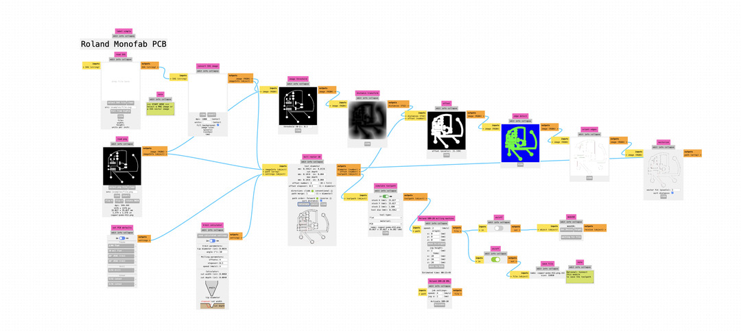
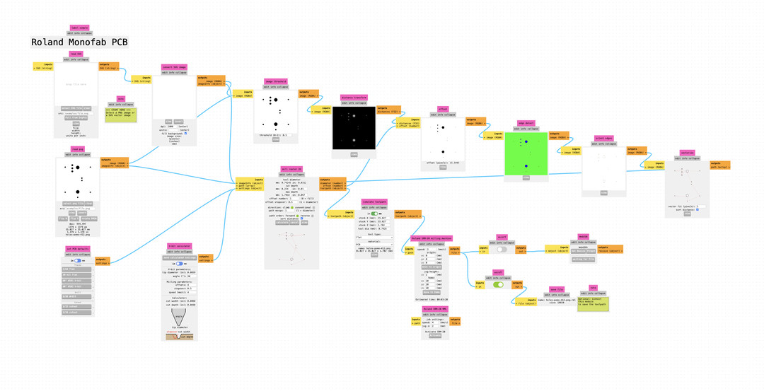
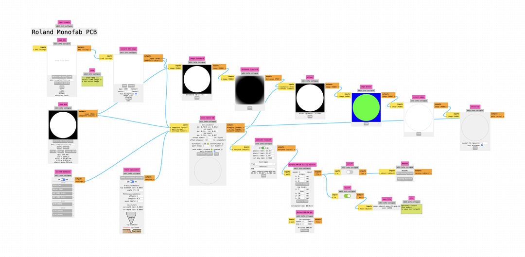
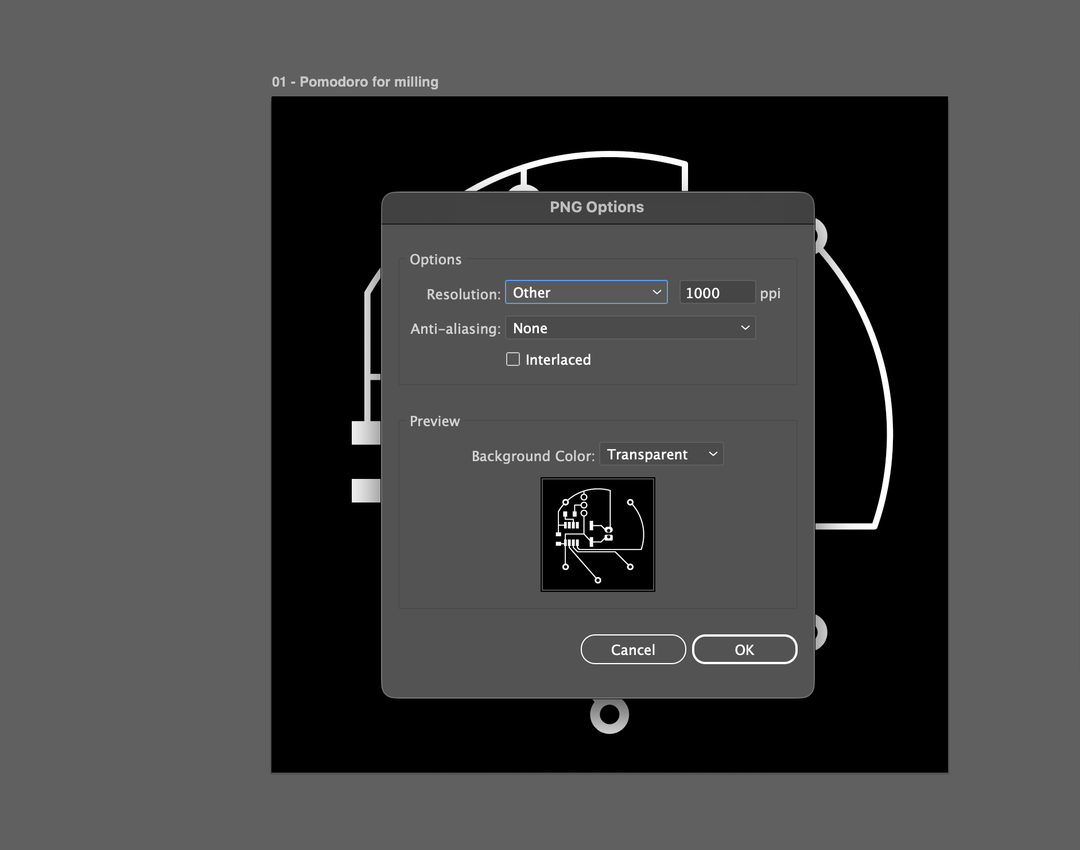
Using the Roland SRM-20 with the MODs project workflow. Settings: speed 2 mm/s, traces at 1/64" bit, outline and holes at 1/32" bit, origin at 0,0,0. The trace layer exports as white on black (white = keep, black = cut away), negative plot.
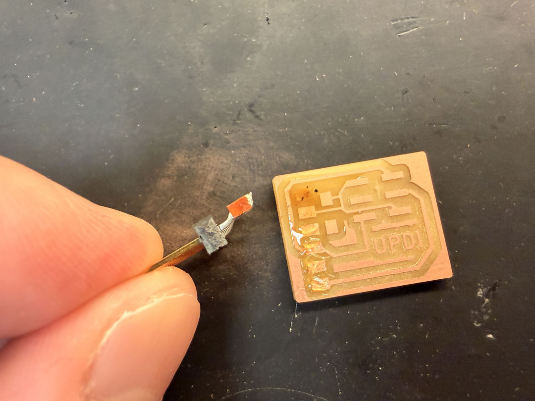
Programming the ATtiny412 happens through that 3-pin UPDI header on the board. UPDI is a single-wire interface, so the programmer's TX and RX both share the same UPDI line, and the 4.7 kΩ series resistor on the board protects PA0 from the two lines fighting each other. The header pinout is VCC / UPDI / GND, with pin 1 marked on the silkscreen so the programmer always plugs in the right way around. Before milling the watch board I soldered up a small UPDI programmer board to use with it. It was good practice on a simpler board.
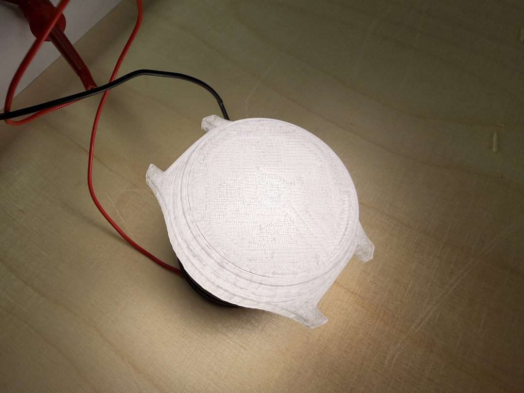
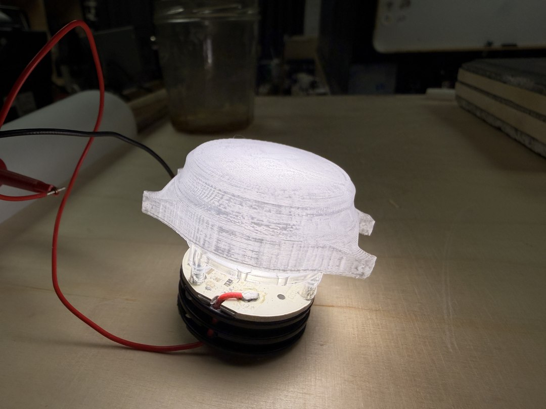
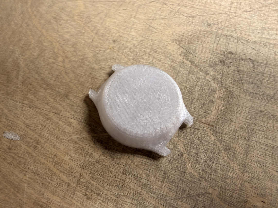
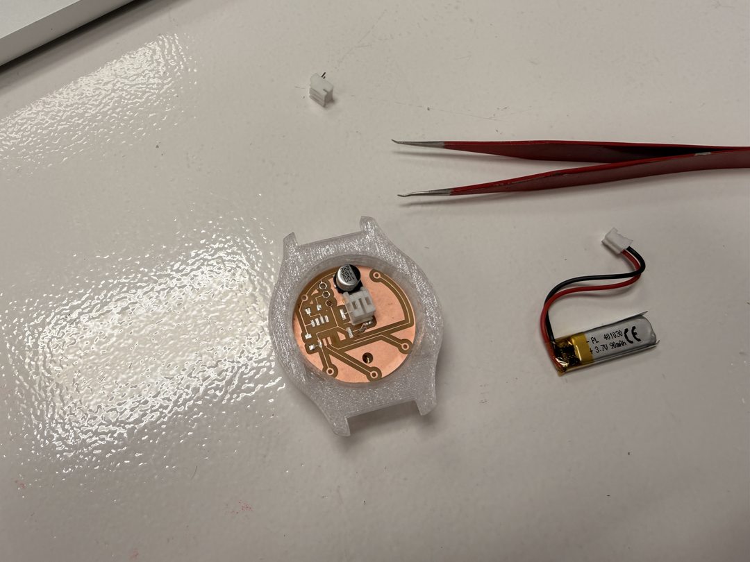
In parallel with refining the PCB, I modelled a 3D printed watch case with lugs. The goal is to have a fully integrated device where the PCB sits flush inside the printed shell.
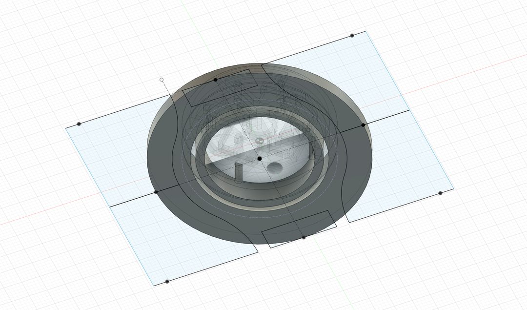
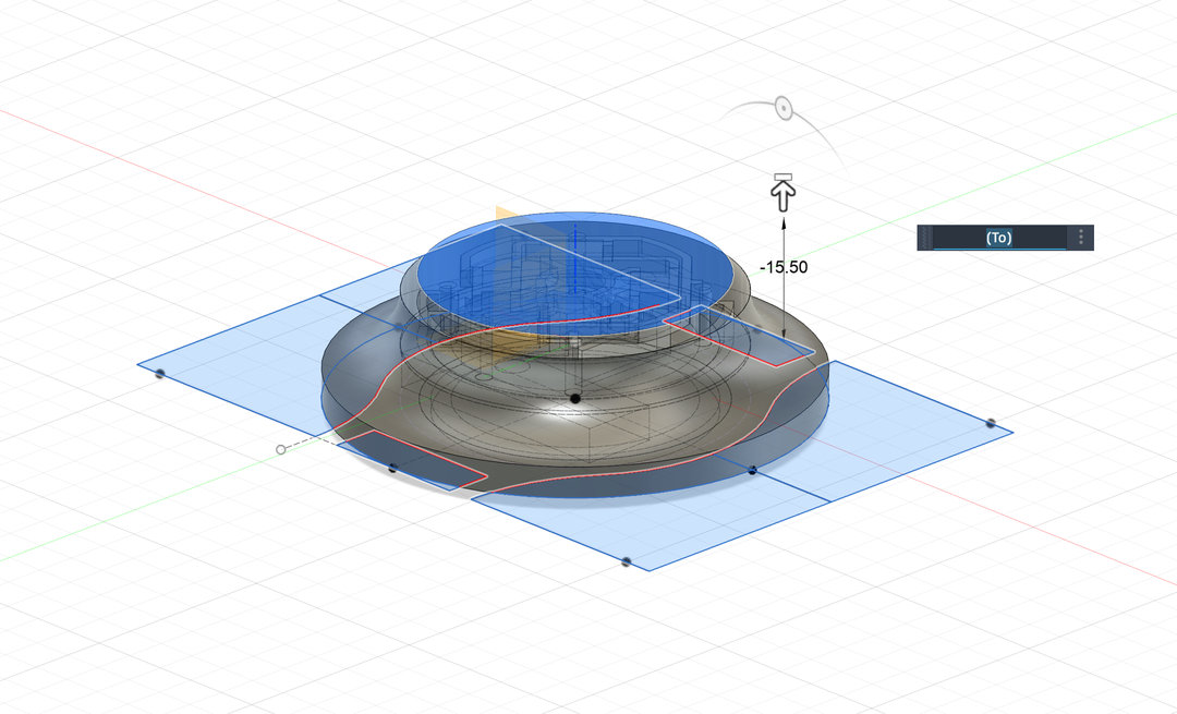
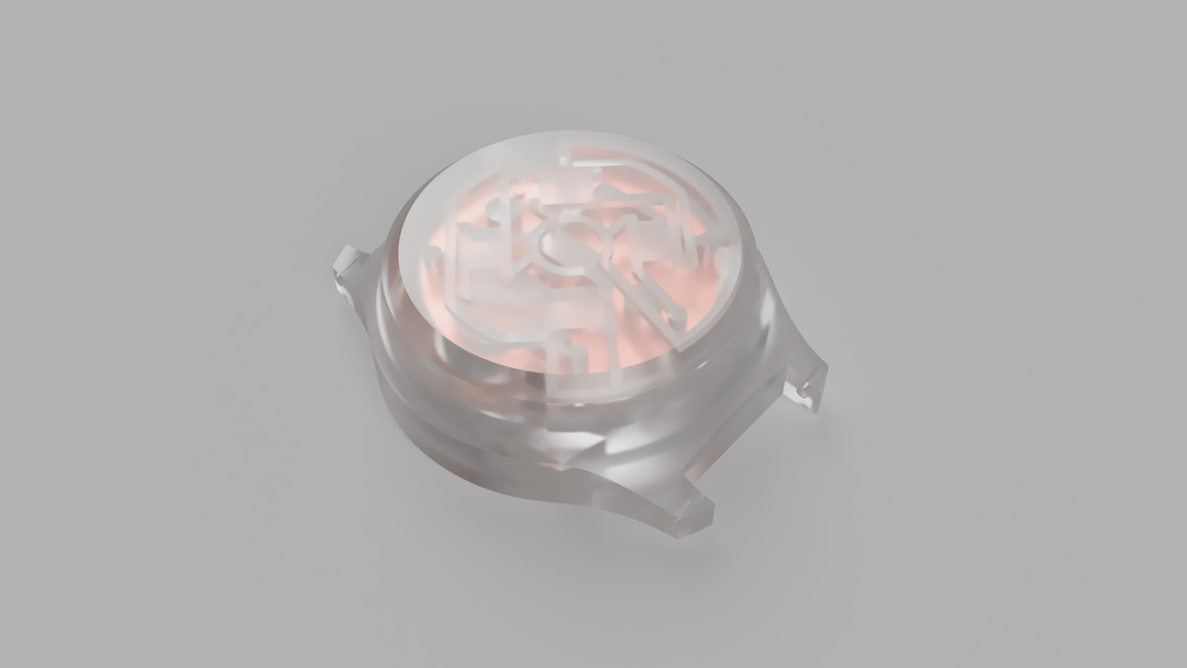
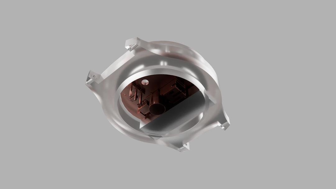
I printed the v2 case and ran some illumination tests to see how light would diffuse through the case material.
KiCad project file of v2 of the watch pomodoro timer
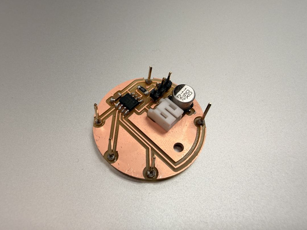
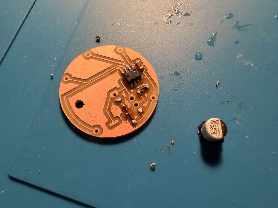
I decided to redesign the board once again. This time, I wanted to move the bulky electrolytic capacitor out of the way to make more room for sliding the LiPo into the watch case. I also repositioned the JST connector for the LiPo.
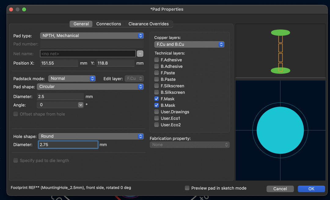
In order to make even more space, I also dropped one of the mounting holes. One would be enough, since the board fits snuggly into the watch housing.
After updating updating the design, I milled the v3 PCB and ran another fit test. It proved to be a bit too tight with the JST connector placement.
KiCad project file of v3 of the watch pomodoro timer
For the final version of my board, I reoriented the JST connector once again by rotating it 90 degrees and running the traces again. This time, there was enough space to slide the battery into the watch housing as to not put any strain on the connector.
KiCad project file of v4 of the watch pomodoro timer
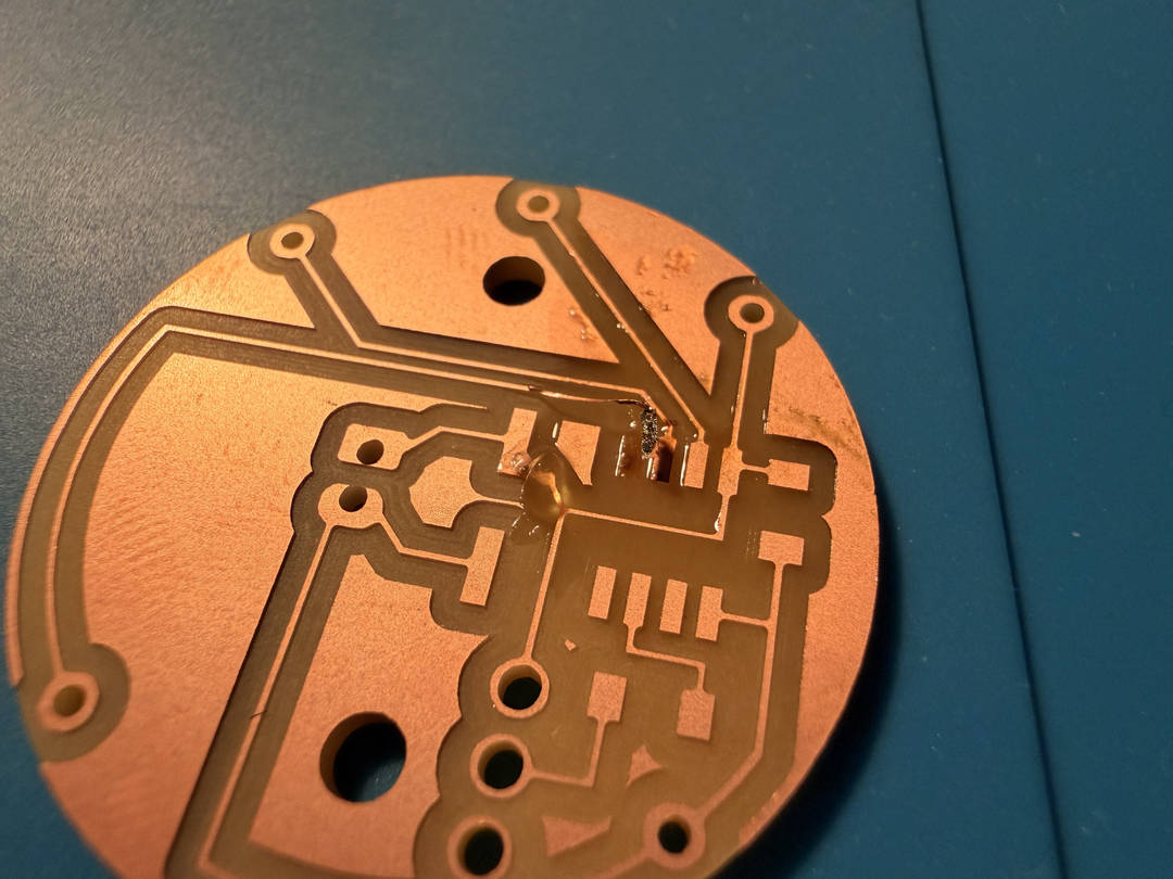
First came a pad lift issue, from applying too much heat. My attempt to fix it with a copper wire was unsuccesful.
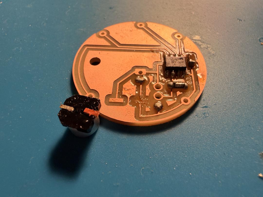
Then came a strange milling depth inconsistency. It was probably due to an issue when setting the z-height on the Roland, although I didn't notice making a mistake in the procedure.
This one was due to my attempt to remove the plastic sleeves from the pins, in order to be able to have more depth (or length) on the connectors.
It was succesfully fixed by using soldering wick to connect the pad to ground (under the electrolytic capacitor).
I had incorrectly believed that a 4.9k resitor could be placed between the UPDI programming connector pin and the pin of the ATtiny412. I had to swap it out for a 0ohm resistor.
After completing the v4 watch board, I ran into trouble when trying to program it. Despite multiple attempts with the UPDI programmer I had built, I was unable to establish a connection with the ATtiny412. The series resistor on the UPDI line had already been swapped out for a 0Ω jumper, the programmer was wired correctly, and the board looked fine under inspection, but the programmer kept timing out. Without a working firmware upload, I couldn't demonstrate the board doing anything functional.
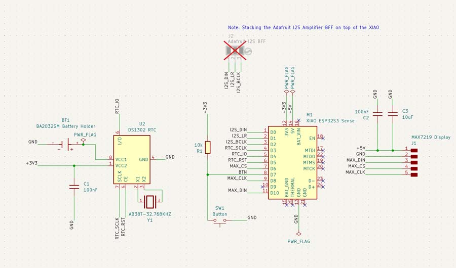
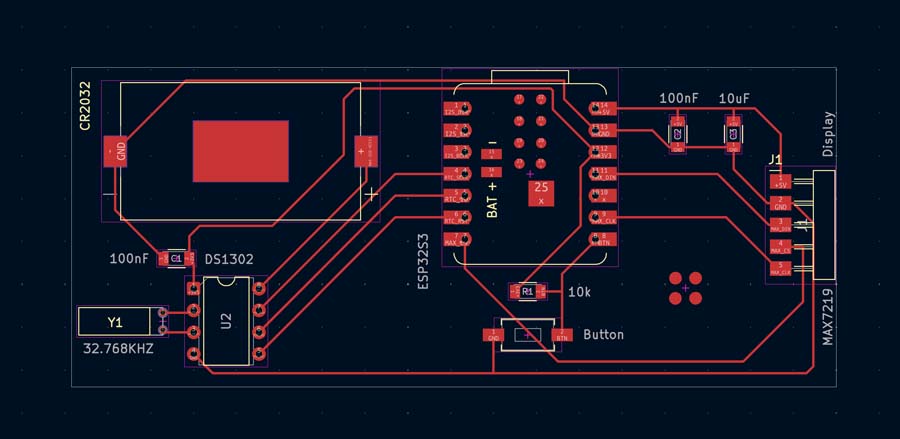
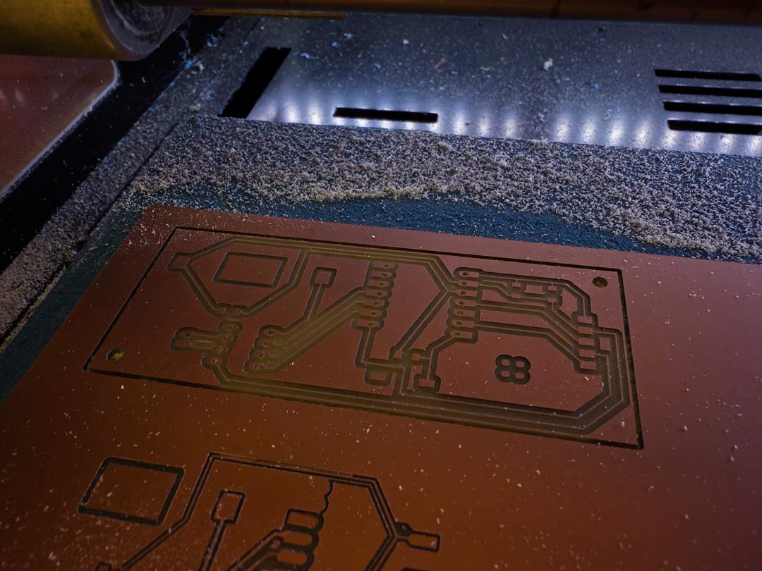
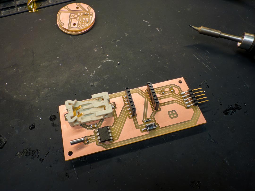
To show a functional board for this week, I'm including the alarm clock PCB I designed in week 06 and soldered up in week 11. It's a more complex board than the watch pomodoro, and it works.
The alarm clock is a custom PCB built around a Seeed XIAO ESP32S3 Sense. The concept is a multimodal alarm clock that uses light, sound, and touch together. The time display is hidden behind a distortion grill, so you have to physically interact with the device to read the time or dismiss the alarm. That friction is intentional: it also stops you from glancing at your phone while trying to sleep.