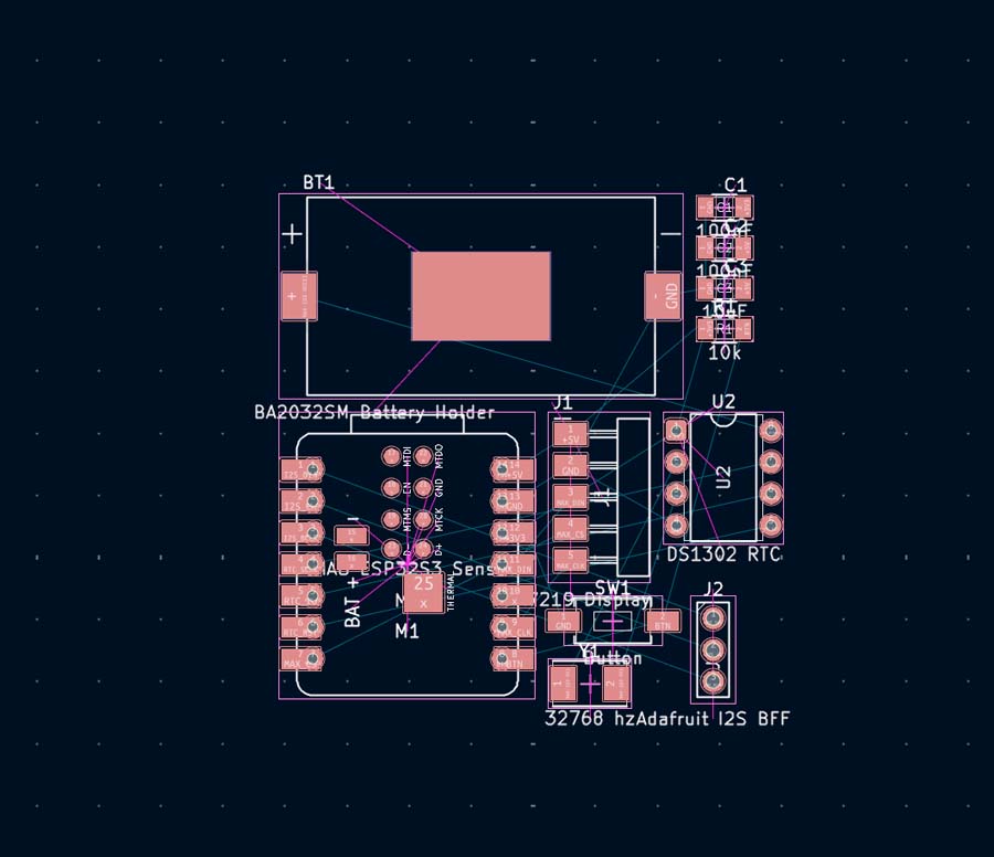
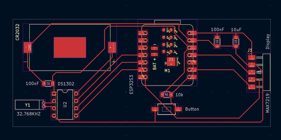
The main thing I worked on this week was designing a preliminary test board for my final project. The concept is still loose, but the core idea is a multimodal alarm clock that uses light, sound, and touch together. The time display is hidden behind a distortion grill: you can't just glance at it. You have to pick it up and wrestle with it to read the time or turn off the alarm. That friction is intentional. It also prevents you from glacing at the time while you're trying to sleep (that's the worst). Still a lot of open questions about the final form, but this test board is a first pass at getting some of the core electronics working together.
Here's what I wanted on the board:
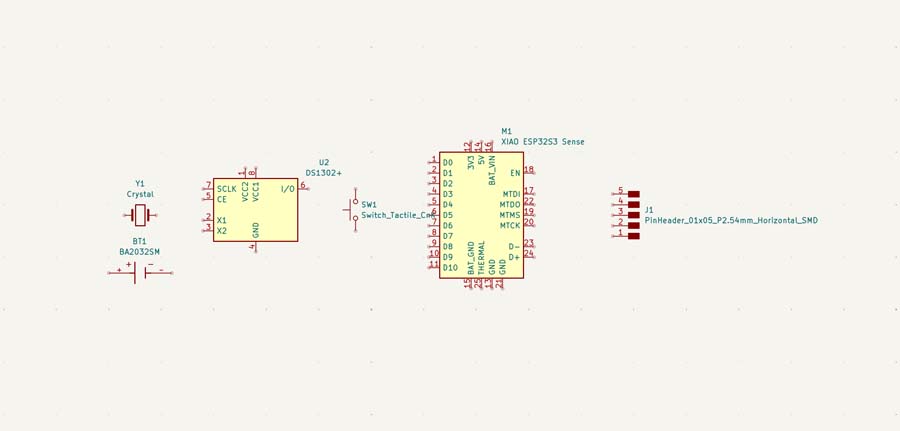
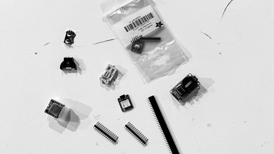
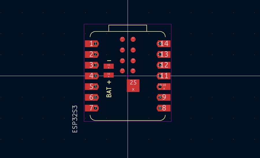
I originally wanted the regular XIAO ESP32S3, but our lab only had the S3 Sense, the C3, and the C6 at the moment. I went with the S3 Sense since it's the most similar. The C6 might be a better fit for the final project, but I didn't want to add more complexity for this first iteration.
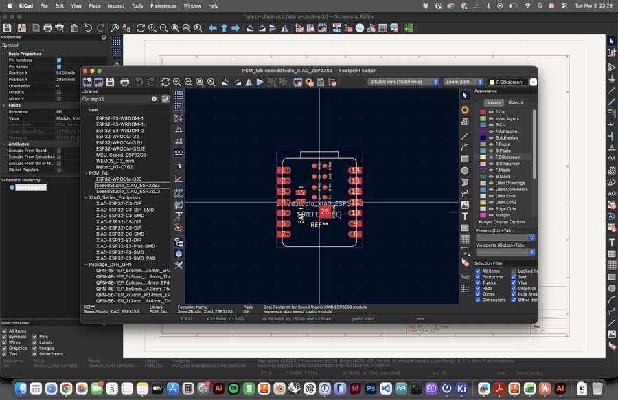
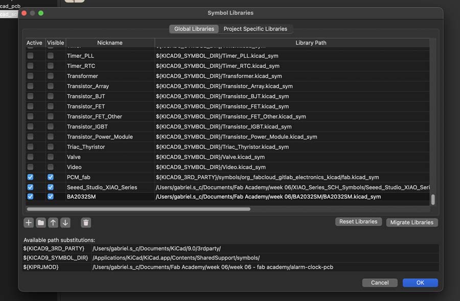
The S3 Sense wasn't in the FabLib KiCad library. My initial plan was to use two 1×7 THT headers, but I found a proper XIAO ESP32S3 symbol and footprint from the FabLib library with named pins so I used that instead since it's identical to the Sense.
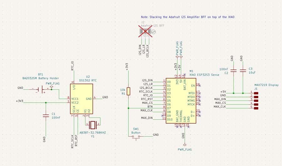
I placed the XIAO at the centre and used net labels throughout to avoid long wires everywhere.
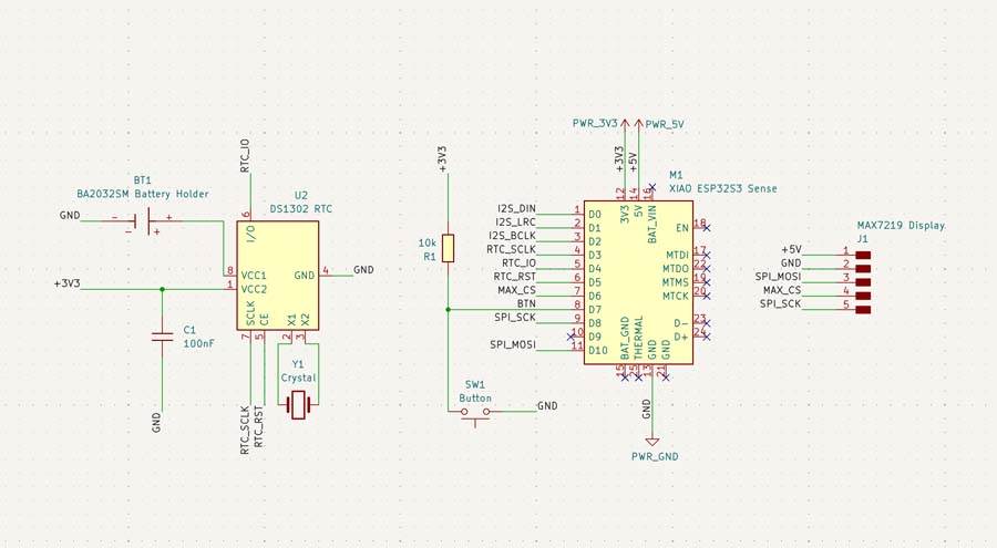
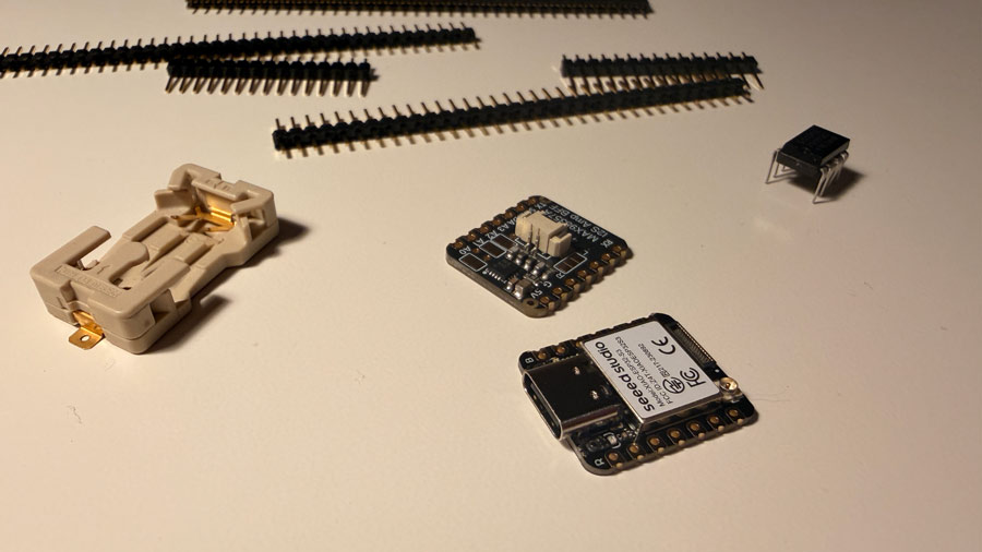
A CR2032 keeps the DS1302 running when the board isn't powered. The BA2032SM is the exact cell holder that I had on hand. I found a proper KiCad symbol and footprint for it, as well as a 3D model.
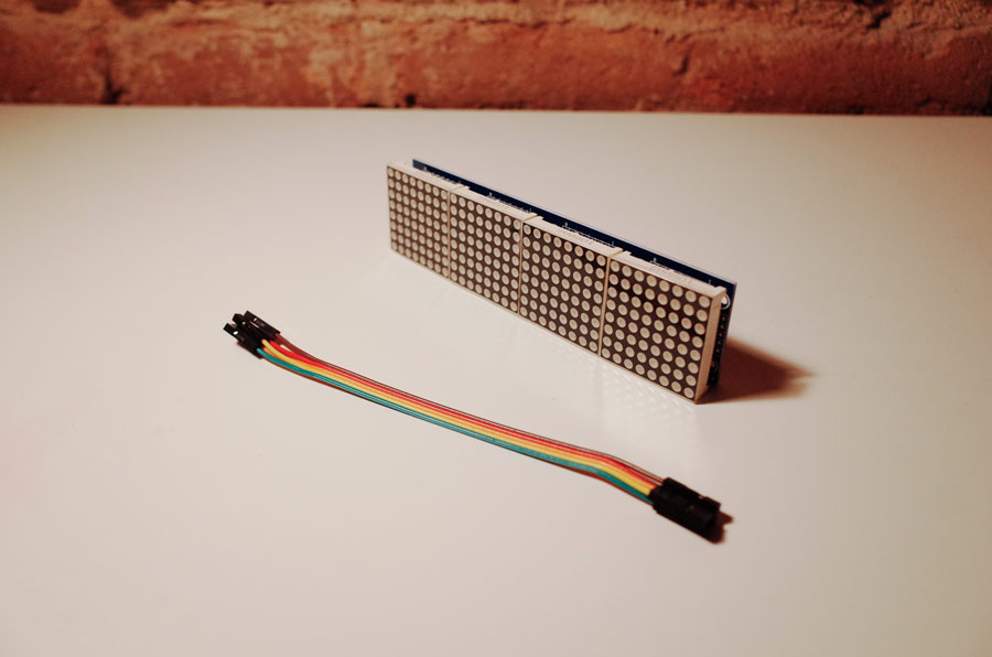
Added a 100nF cap near the DS1302's VCC2 pin for stability, based on my research. For the MAX7219, the datasheet says to put a 10μF electrolytic and a 0.1μF ceramic cap between V+ and GND as close to the chip as possible to handle peak current draw from the digit drivers.
"To minimize power-supply ripple due to the peak digit driver currents, connect a 10μF electrolytic and a 0.1μF ceramic capacitor between V+ and GND as close to the device as possible. The MAX7219/MAX7221 should be placed in close proximity to the LED display, and connections should be kept as short as possible to minimize the effects of wiring inductance and electro-magnetic interference. Also, both GND pins must be connected to ground.”
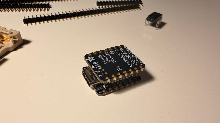
The BFF stacks directly on the back of the XIAO so it doesn't need its own connector in the schematic. I just added a text note for the I2S connectors.
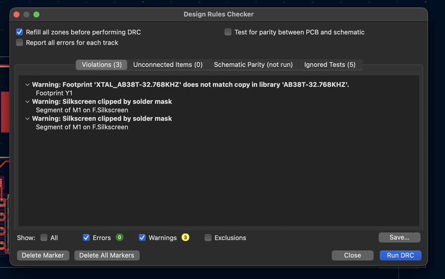
KiCad's ERC needs every power net to have at least one power output pin driving it, otherwise it throws errors. At first I used the FabLib PWR_3V3, PWR_5V, and PWR_GND symbols.
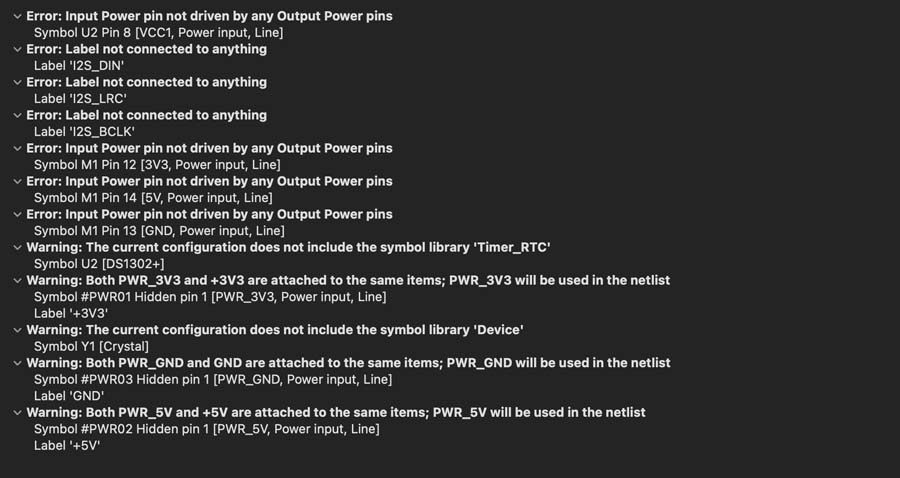
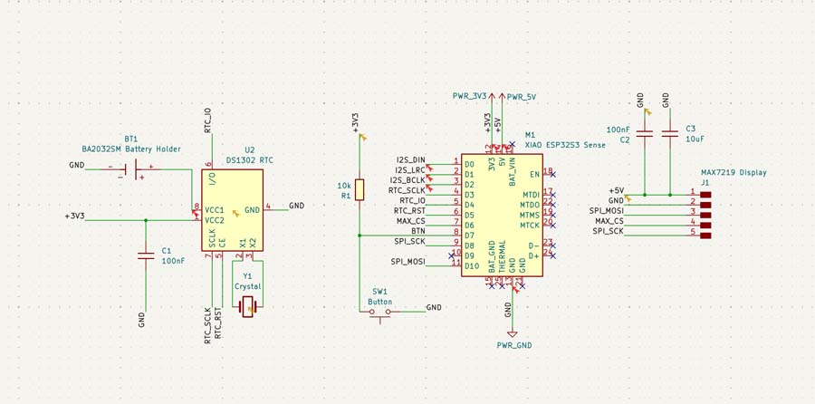
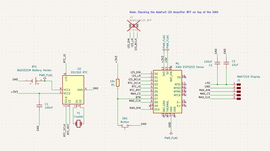
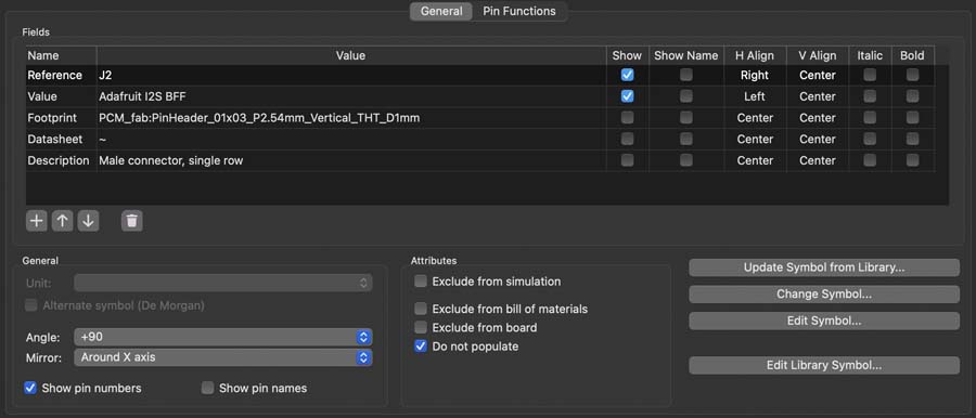
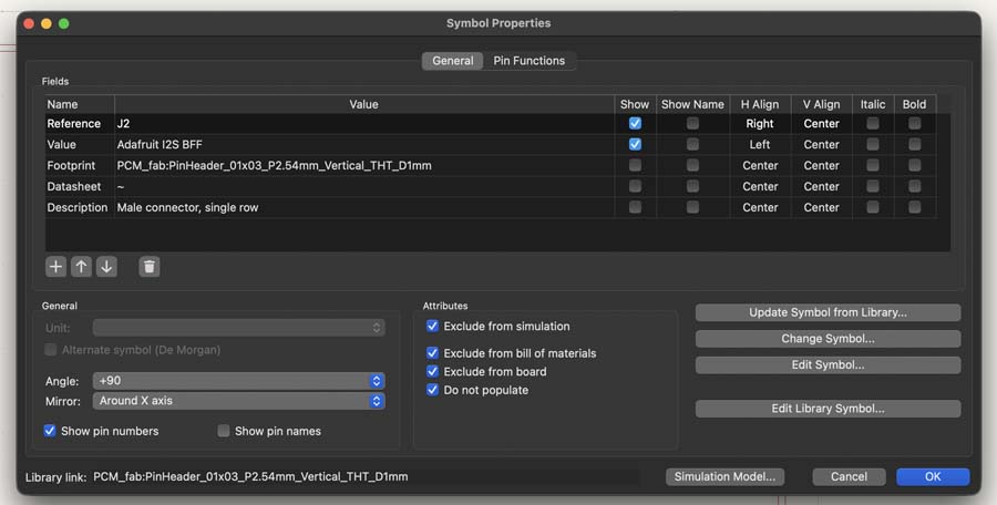
I added proper PWR_Flags to all power rails, instead of the FabLib PWR_3V3, PWR_5V, and PWR_GND. I also added a 1x3 pinheader in order to be able to connect the I2S pins from the XIAO to something real. However, I checked the do not populate box.
The standard KiCad Crystal symbol had no footprint when I tried to push the schematic to the PCB.
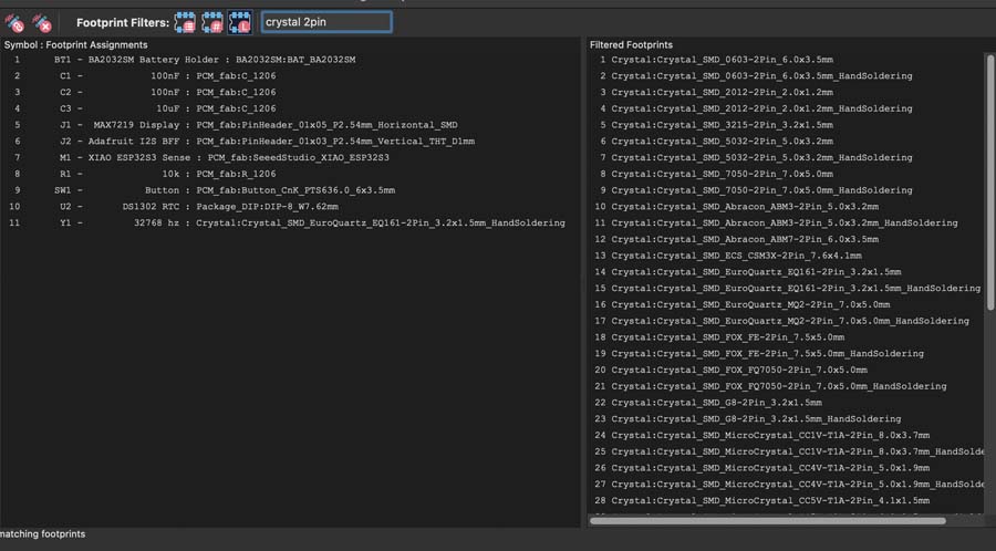
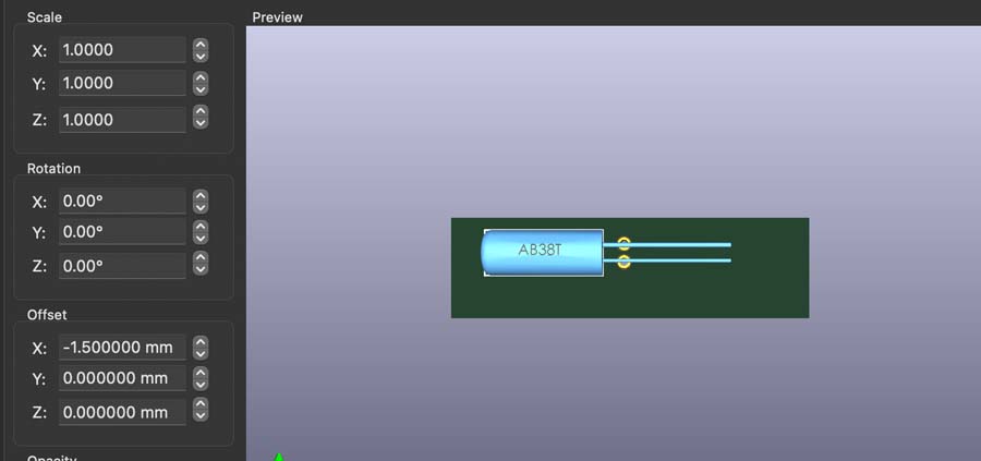
The Abracon AB38T and ABS07 seemed quite popular and easy to find in my searches on DigKey, Mouser, and Google.
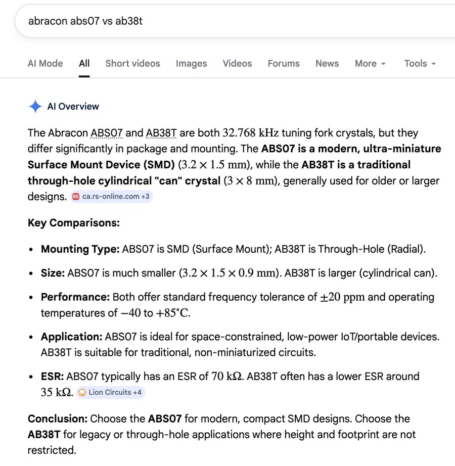
I went with the AB38T specifically because the through-hole pads are easier to hand solder vs the tiny Abracon ABS07.
I ended up finding the Abracon AB38T-32.768KHz footprint, schematic, and 3D model on SnapEDA.
Trying do not populate didn't end up removing the 1x3 pinheader when I populated my footprint.
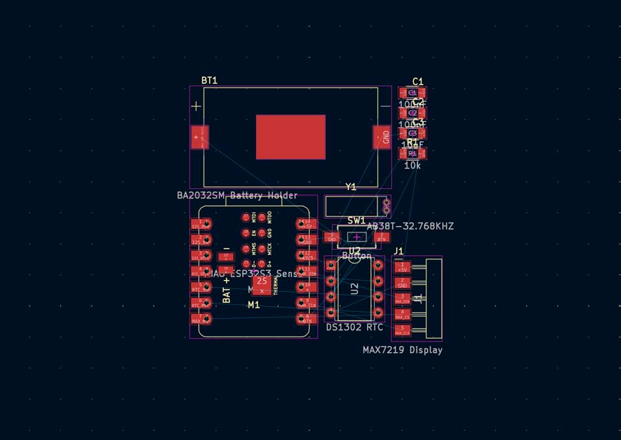
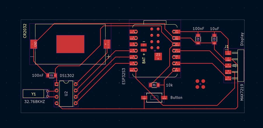
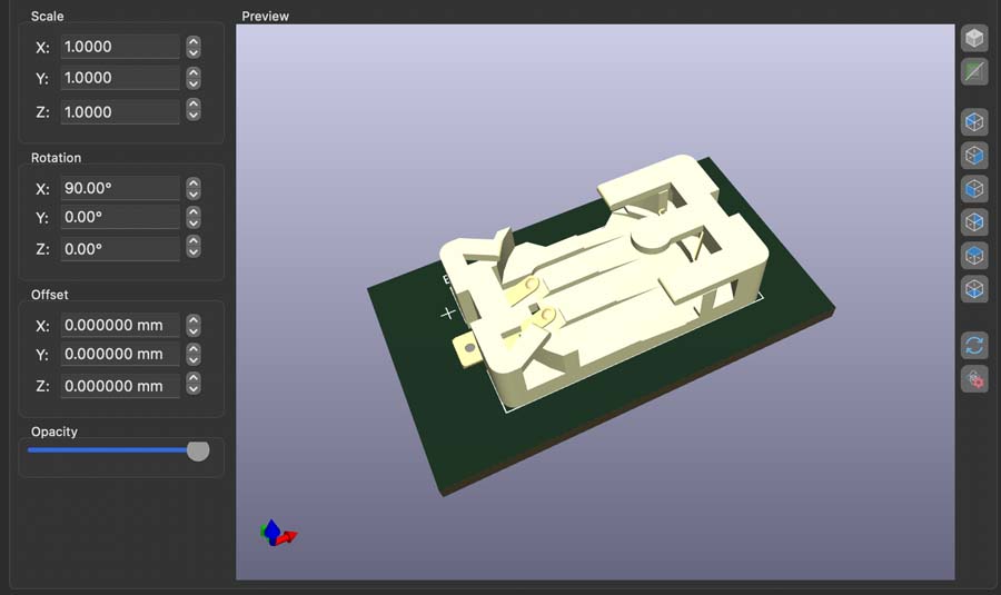
I first removed or relocated all the silkscreen text that was causing issues. I won't be using any of the pads under the ESP32 and it will be floating above the board.
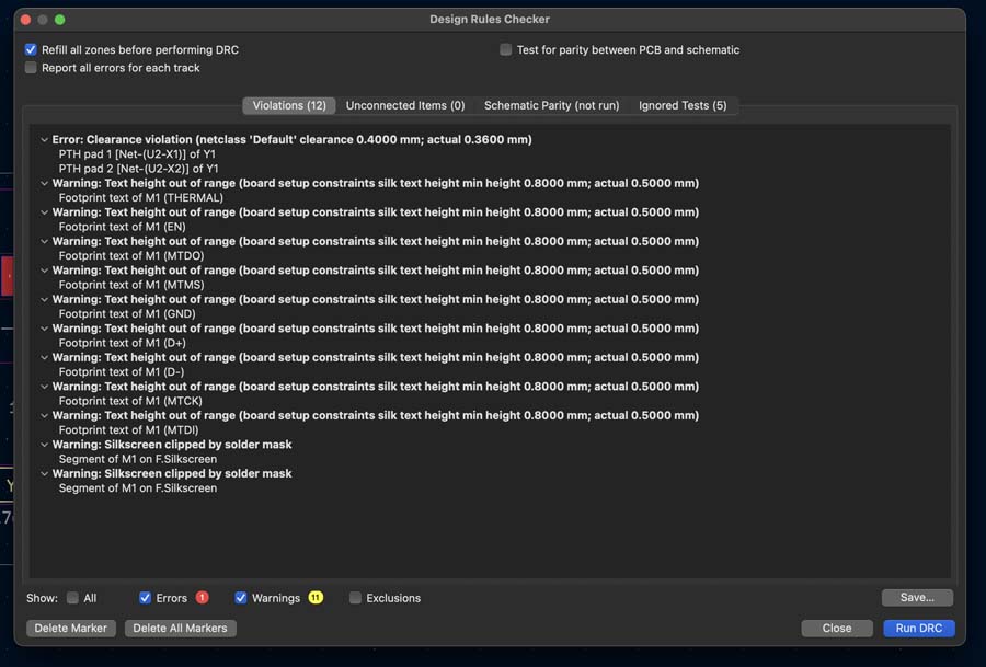
I also had to space out the holes for the crystal because our holes are larger when using our in house fab. The design of the AB38T uses two leads so it shouldn't be a problem.
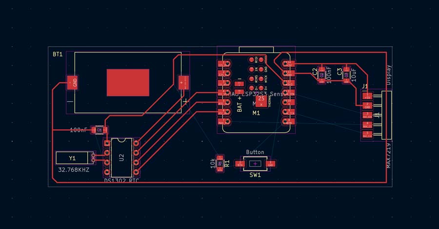
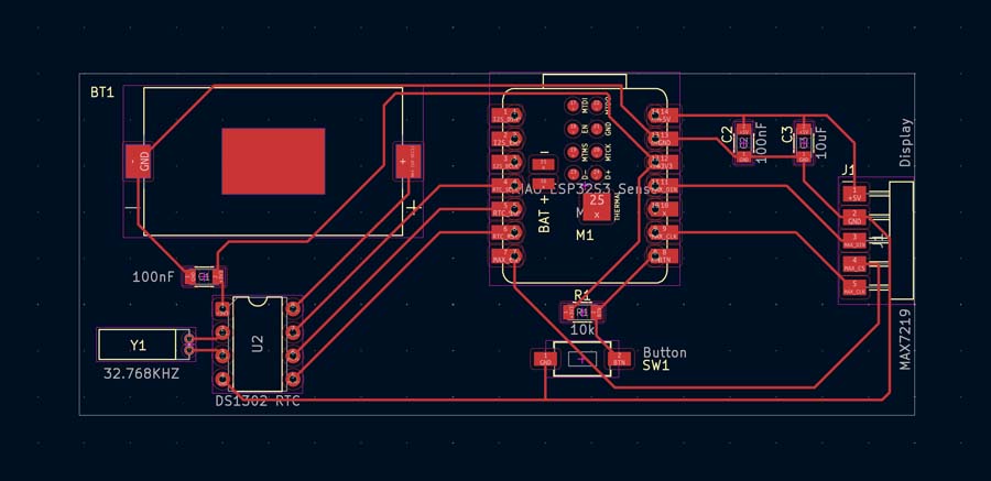
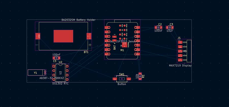
I tried two different ways of routing the ground trace.