8. Electronics Production
Group Assignment
Characterize the design rules for your in-house PCB production process.
Our Fab Lab has a Roland SRM-20, which I will be using to mill my board.
Trace Width and Spacing
Minimum Trace Width: the narrowest trace that could be milled without detaching from the substrate was 0.13mm. This is the minimum functional width, though using wider traces is recommended to ensure greater durability and adhesion.
Minimum Trace Spacing: The smallest reliable gap between adjacent traces was 0.16mm. Tighter spacing may result in bridging or incomplete isolation.
Milling Settings
Milling Speed: a constant speed of 10mm was used for both trace and edge milling
Feed Rate: the feed speed was maintained at 4mm/s during the milling process.
Cut Depth: trace depth of 0.1016mm and outline depth of 0.6096mm.
In KiCad, I made sure to make all traces at least 0.4 mm wide because with anything smaller, the 0.4mm cutting bit won’t be able to fit between them.
Exporting KiCad Files
For this week, I used my week 6 design. I first exported the traces and edges as 2 SVG files. Start by navigating to File>Plot. In the format dropdown menu, select SVG as the output format.
Week 6
Under the “Include Layers” section, make sure that only F.Cu (Front Copper) and Edge.Cuts (Board Outline) are selected.
Lastly, at the top of the dialog, you specify where the files will be saved by setting the Output Directory. Once complete, click Plot. This generateds two separate SVG files: one for the front copper layer and one for the board outline.
Converting SVG to PNG
Use Adobe Illustrator to edit the saved SVG files and save as PNGs. After opening the Edge.Cut file in Illustrator, I ungrouped each part and filled in the board outline white. After filling, I grouped the black and white portions back together. I then opened the F.Cu file and grouped all the pieces together. After combining the outline and traces, I used the align tool to center the layers both vertically and horizontally. To export, I hid one layer and pressed File>Export>Export As>Export as PNG. Do the same with the other layer.
Edge Cuts

Traces

Preparations
I prepared my file for machining using Mods Web App. To start using Mods Web App, right click and select Programs>Open Programs. Once in the menu, I was guided by a fellow classmate on what comes next. Scroll down to where it says Roland and under that, select mill 2D PCB. This opens up to a new page requiring changed settings.
Roland Monofab PCB Program Setup
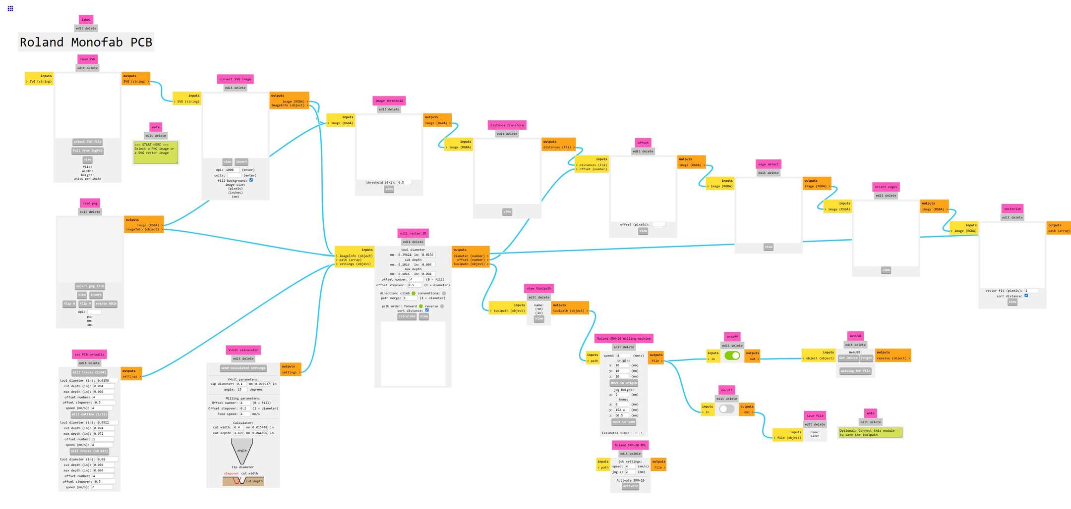
First, import as a PNG file. In the option of whether milling the trace or outline, that depends on which file you choose, though both will be done eventually.
Next, change the speed and location for the milling. Speed of ten and X,Y,Z to 0. Change the On/Off switch connected to WebUSB to Off and the On/Off switch below to On.
Lastly, in the middle of the screen, click the calculate box which saves it as an RML file.
Machining
Once the files are created, the milling can begin. To machine the board, first secure the FR1 Copper Clad sheet to the machine bed. This was done using double sided tape, carefulling ensuring the tape is even with no bumps. Next, you need to put in the end mill. Using VPanel SRM-20, I positioned the spindle upwards to make putting in an end mill easier.
Then jog the bit to the correct position you want the X,Y,Z=0, 0 position to be. Then hit the XY Zero button.
VPanel SRM-20 Setup
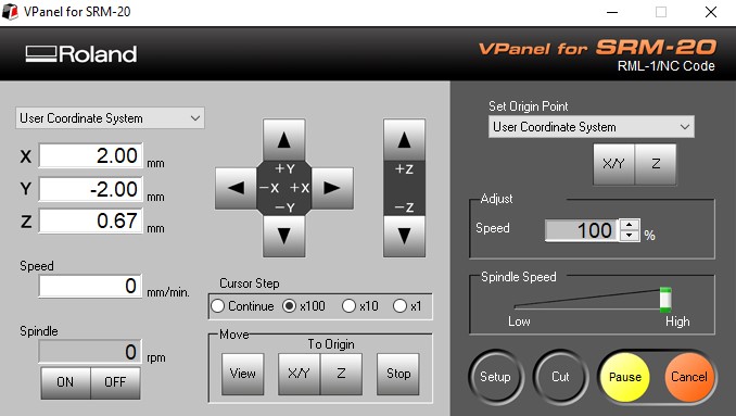
I then moved the spindle down so that the end mill sat just above the top right corner of the copper. To set the Z-zero, I then let the tip slide to just touch the material. I then slightly moved the spindle down and set the origin point. I then moved the spindle up slightly after tightening in the end mill bit. Make sure the lid is closed and start milling. Use the 0.4mm end mill to cut the traces and the 0.8mm end mill to perform the edge cuts.
Milling Board
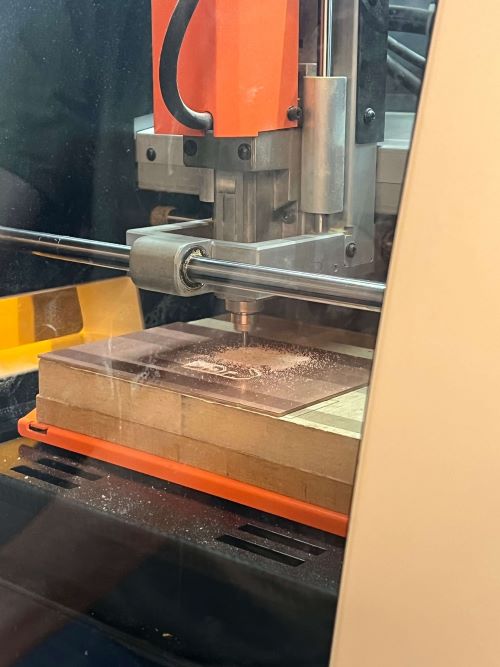
I then vacuumed the dust away and removed my milled board.
Soldering
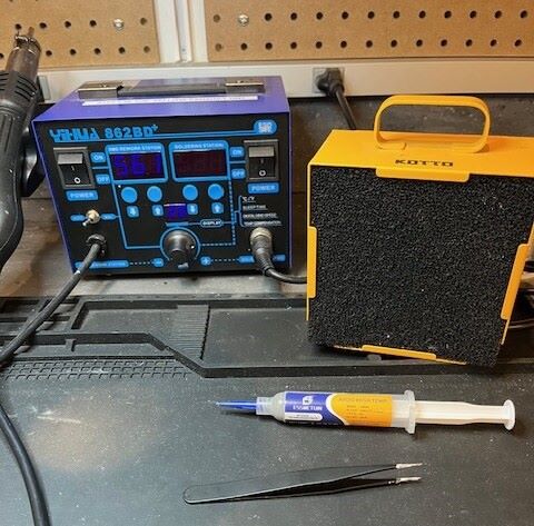
It’s now time to solder! I used my KiCad design as a reference when finding the components needed and during the assembly process. I used solder paste to mount each component, using the heat gun until the paste turns silver. That is its solid state.
Solder Station
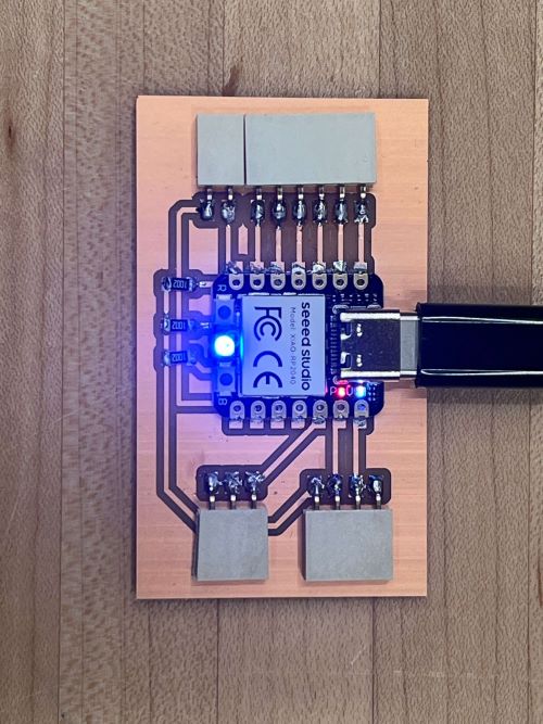
Final Circuit Board
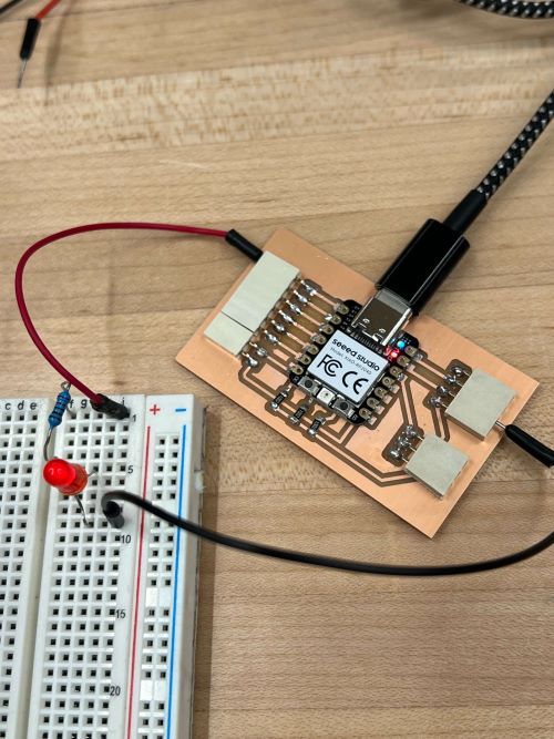
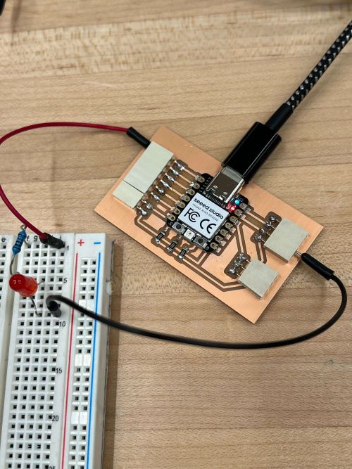
Testing
Now that the board is complete, it’s time to test it! I completed a basic blinking led function using a separate breadboard and some basic code found on the arduino website.
Blinking Light On
Blinking Light Off
Basic Code
        /*
  Blink

  Turns an LED on for one second, then off for one second, repeatedly.

  Most Arduinos have an on-board LED you can control. On the UNO, MEGA and ZERO
  it is attached to digital pin 13, on MKR1000 on pin 6. LED_BUILTIN is set to
  the correct LED pin independent of which board is used.
  If you want to know what pin the on-board LED is connected to on your Arduino
  model, check the Technical Specs of your board at:
  https://www.arduino.cc/en/Main/Products

  modified 8 May 2014
  by Scott Fitzgerald
  modified 2 Sep 2016
  by Arturo Guadalupi
  modified 8 Sep 2016
  by Colby Newman

  This example code is in the public domain.

  https://www.arduino.cc/en/Tutorial/BuiltInExamples/Blink
*/

// the setup function runs once when you press reset or power the board
void setup() {
  // initialize digital pin LED_BUILTIN as an output.
  pinMode(LED_BUILTIN, OUTPUT);
}

// the loop function runs over and over again forever
void loop() {
  digitalWrite(LED_BUILTIN, HIGH);  // turn the LED on (HIGH is the voltage level)
  delay(1000);                      // wait for a second
  digitalWrite(LED_BUILTIN, LOW);   // turn the LED off by making the voltage LOW
  delay(1000);                      // wait for a second
}