Input Devices
Learning Experience
During this assignment, I gained extensive hands-on experience in integrating sensors, designing printed circuit boards (PCBs), and programming microcontrollers. I explored various temperature sensors and light-dependent resistors (LDRs), gaining a thorough understanding of their working principles and how they interact with microcontrollers such as the XIAO ESP32-C3. To deepen my learning, I designed a custom PCB using KiCad, where I creatively implemented an octopus-inspired layout. I then successfully fabricated the board using the SRM-20 milling machine. Following this, I assembled the circuit by carefully soldering all the components and accurately placing them on the board. Using the Arduino IDE, I developed and uploaded a program that enabled sensor-based control of an LED, which added a practical dimension to the theoretical knowledge. While working on this, I encountered and resolved issues such as I2C device detection errors, which significantly enhanced my troubleshooting and problem-solving skills. Overall, this assignment strengthened my understanding of analog and digital signals, circuit design, and real-world sensor applications, equipping me with the confidence and competence to tackle more advanced electronics projects in the future.
Key Accomplishments
✅Successfully combined and tested the XIAO ESP32-C3 with LDR sensors.
✅Created a unique PCB in KiCad with an inventive octopus-shaped architecture and sensor connections.
✅Created Gerber files, transformed them into G-code, then used SRM-20 to mill PCBs.
✅Finished component placement and soldering, guaranteeing a completely working circuit.
✅To process sensor data and control an LED based on light intensity, I wrote and uploaded Arduino ID code.
✅I2C device detection problems were debugged and fixed, enhancing circuit troubleshooting abilities.
✅Used the Serial Monitor in Arduino IDE for real-time data monitoring and validation.
✅Recognized the distinctions between digital and analog signals and how they are used in sensor-based systems.
✅successfully recorded every step of the process, including debugging, programming, manufacture, and design.
Task: Input Devices
Group assignment:
Probe an input device(s)'s analog levels and digital signals
Document your work on the group work page and reflect on your individual page what you learned
Individual project:
Measure something: add a sensor to a microcontroller board that you have designed and read it.
Individual Assignment:
As part of my Individual Assignment, I chose to explore and experiment with a variety of temperature sensors and Light Dependent Resistors (LDRs). To analyze their behavior and output, I utilized the Serial Monitor in the Arduino IDE, which allowed me to observe real-time data readings. Additionally, I planned to integrate one of these sensors directly into my custom-designed board, thereby enabling it to function as an input device within a larger embedded system.
What is a Sensor?
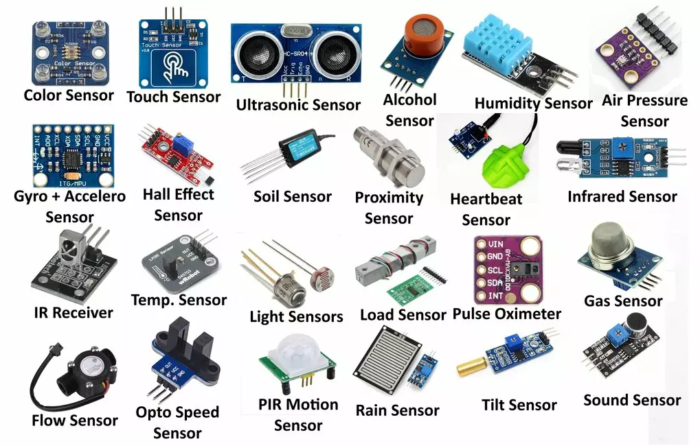
A sensor is an electronic device that detects changes in the physical environment and converts them into electrical signals. These signals are then processed to provide meaningful digital output. Sensors are capable of detecting a wide range of physical parameters such as temperature, light, sound, pressure, motion, and magnetic fields. They play a vital role in modern technology by enabling machines and systems to perceive and respond to their surroundings.
The output generated by a sensor can be used for monitoring, automation, or controlling other devices. Typically, the information collected is displayed on a screen or transmitted to other systems for further analysis.
Image: Types of Sensors
Sensors in Smartphones
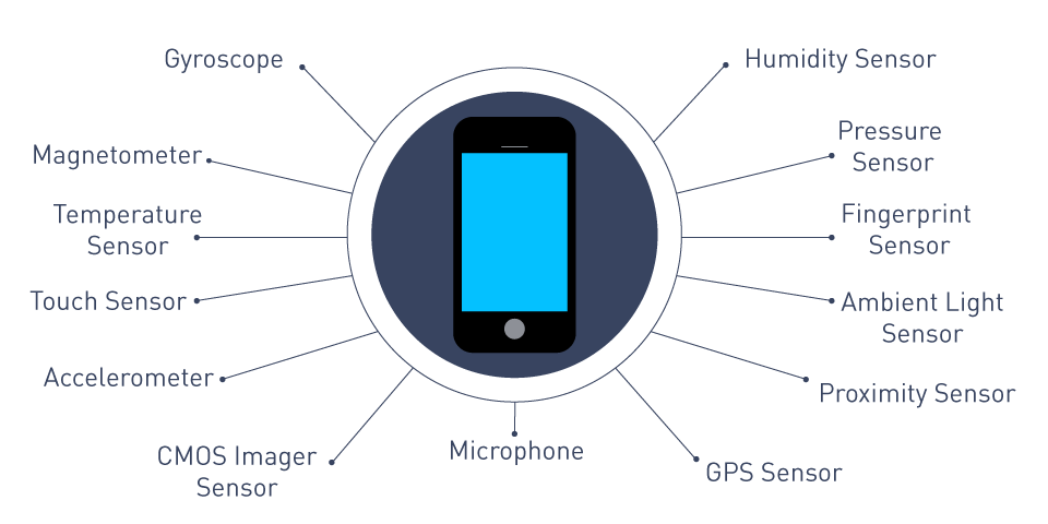
Modern smartphones are equipped with multiple sensors to enhance functionality and user experience. These include accelerometers, gyroscopes, proximity sensors, ambient light sensors, fingerprint sensors, magnetometers, and more. Each sensor has a specific role, such as detecting orientation, light levels, or touch, enabling advanced features like auto-rotate, facial recognition, and screen brightness adjustment.
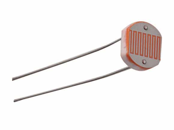
LDR Sensor (Light Dependent Resistor)
A Light Dependent Resistor (LDR), also known as a photoresistor, is an electronic component that changes its resistance based on the intensity of light falling on it. When the light intensity increases, its resistance decreases, and vice versa. This unique characteristic makes it ideal for designing circuits that respond to varying light conditions, such as automatic street lights or light-sensitive alarms.
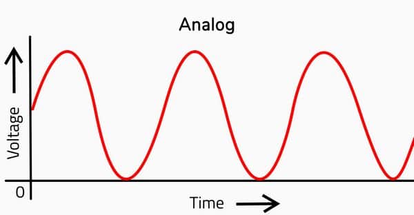
Analog Signal
An analog signal is a continuous signal that can represent an infinite number of values within a specific range. It varies smoothly over time and closely resembles the actual quantity it measures, such as sound, temperature, or light intensity. Analog signals are commonly found in natural phenomena and are used in many electronic devices.
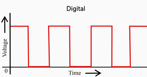
Digital Signal
In contrast to analog signals, digital signals consist of discrete values. These signals operate using binary states—either ‘HIGH’ (1) or ‘LOW’ (0). Digital signals are widely used in modern electronics and computing because they are easier to store, transmit, and process with high accuracy.
 Reference Website
PCB Design
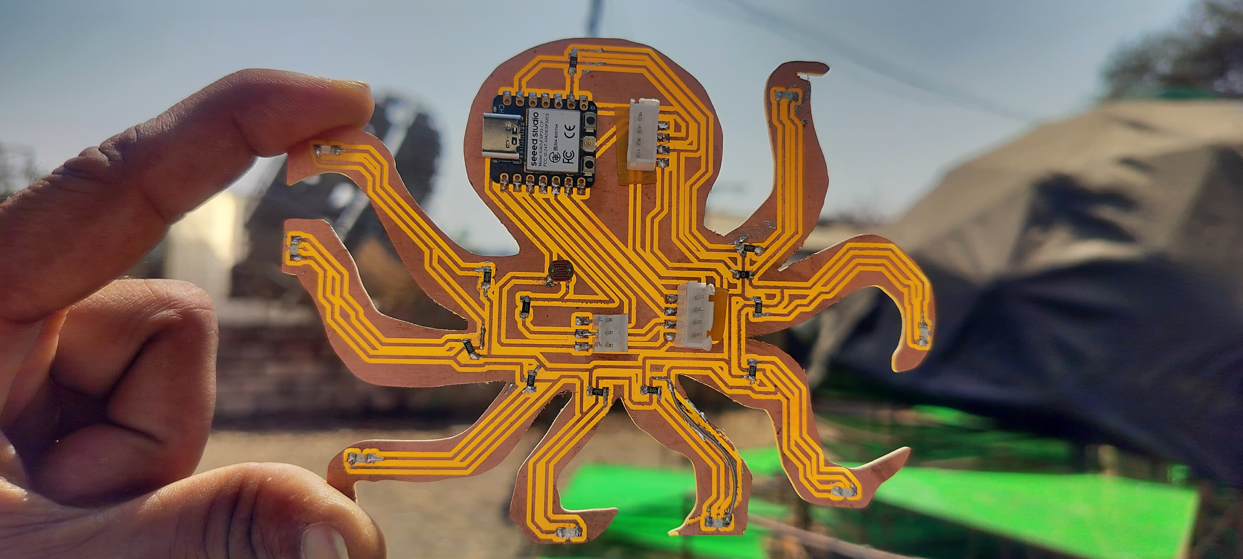
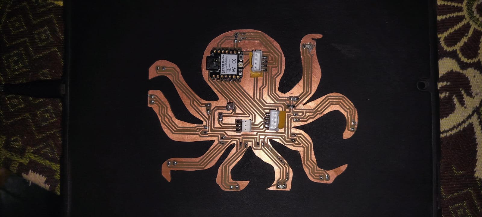
For my input device assignment, I decided to design a custom PCB that integrates an LDR (Light Dependent Resistor) sensor. The purpose of this board is to observe and analyze how both analog and digital signals behave within the same circuit environment. To give my PCB a distinctive and creative look, I chose an octopus-shaped design layout.
You can also refer to my previous assignment where I explored basic PCB designing techniques.
One of the key things I discovered during this process is that integrating an image into PCB design can help customize the board layout in a unique and visually appealing way.

I began by downloading an octopus-themed image from a search engine that would serve as the inspiration for my PCB outline.
Next, I opened KiCad and used the built-in Image Converter tool to prepare the image for PCB use.
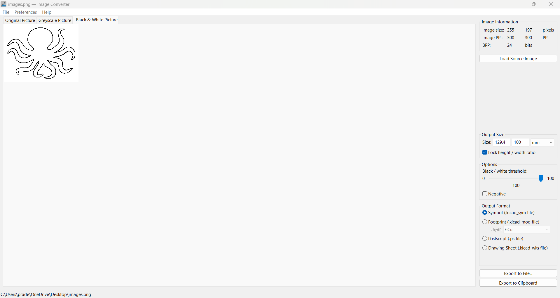
Within the file menu, I uploaded the octopus image and adjusted the output size parameters—setting the width between 100 to 129 mm—to align with my board dimensions.
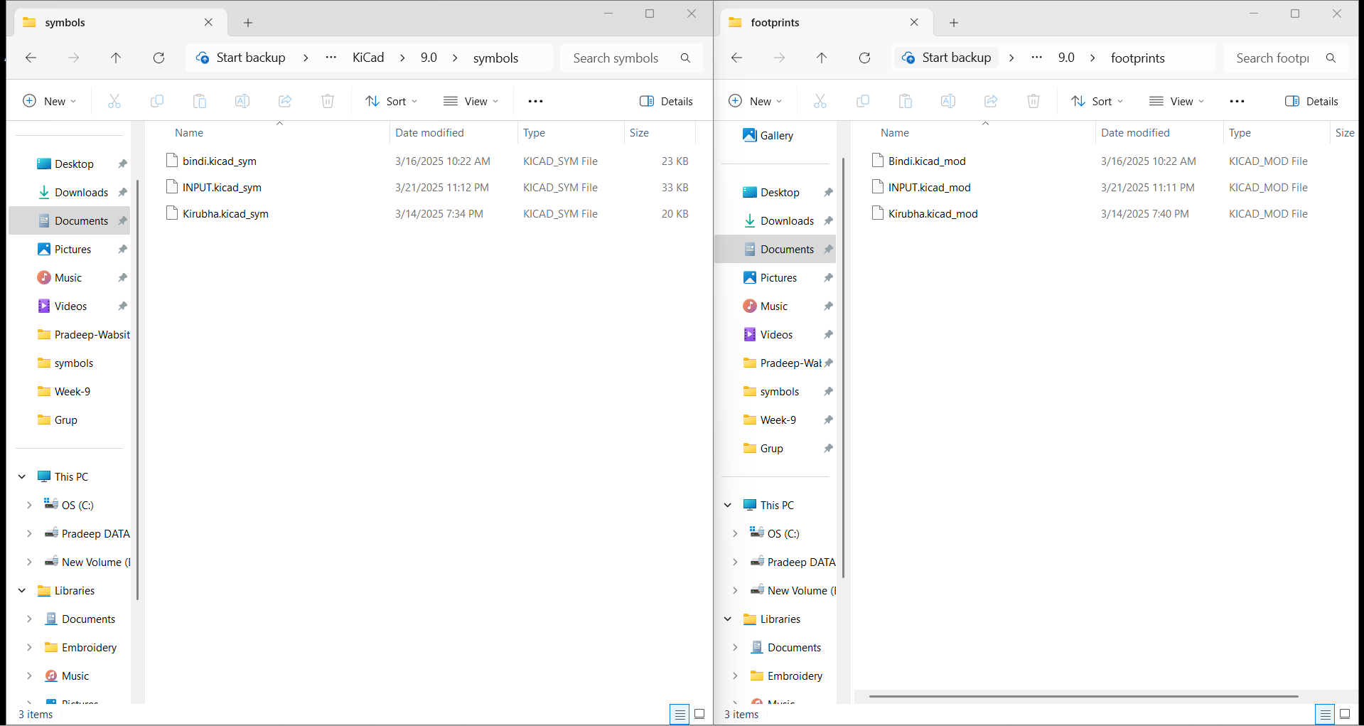
After setting the size, I exported both the symbol file and footprint (.mod) file and saved them in the KiCad project folder for further use.
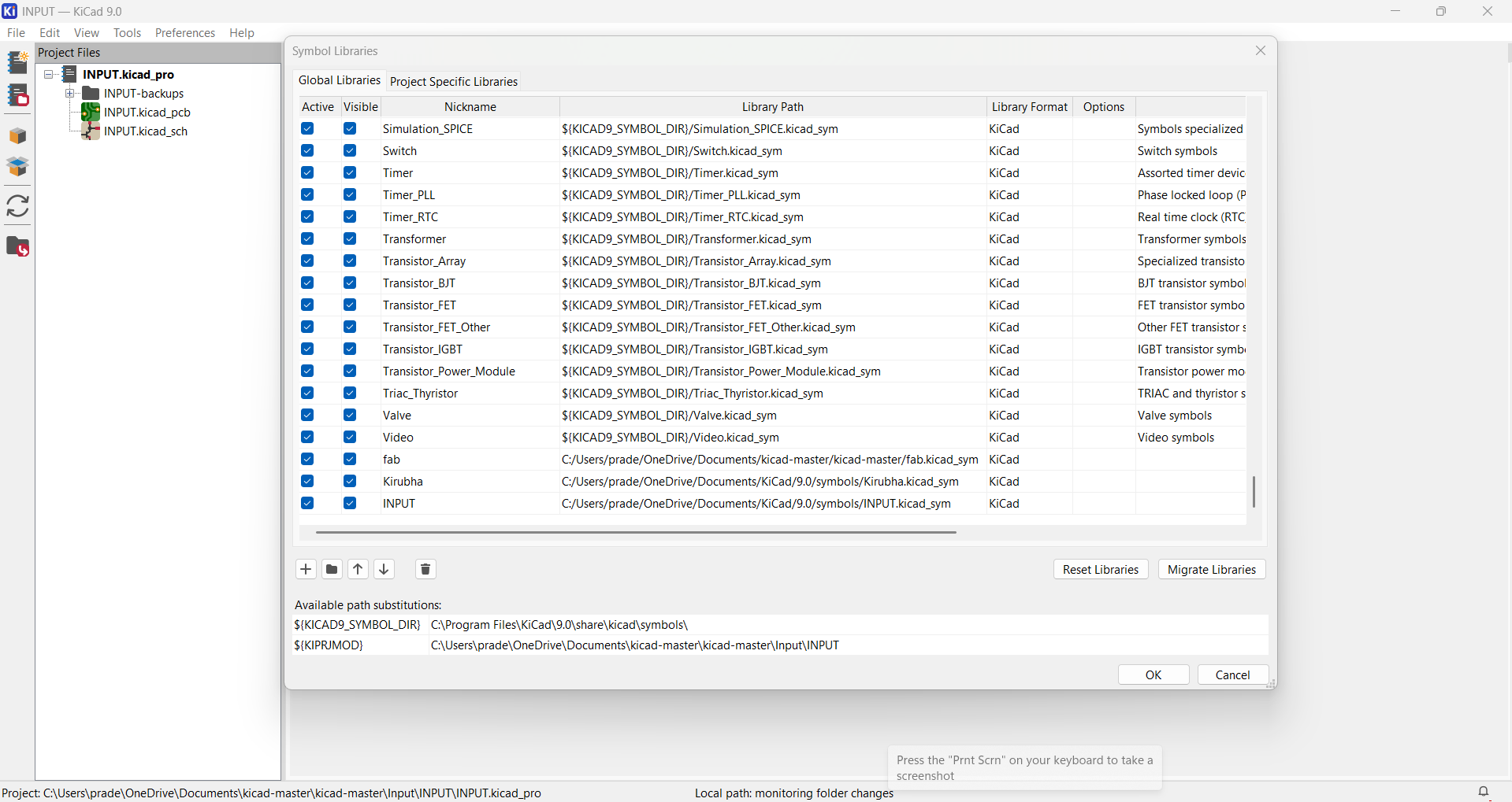
I then navigated to the Preferences section in KiCad and added my custom symbol library under the "Symbol Libraries" tab.
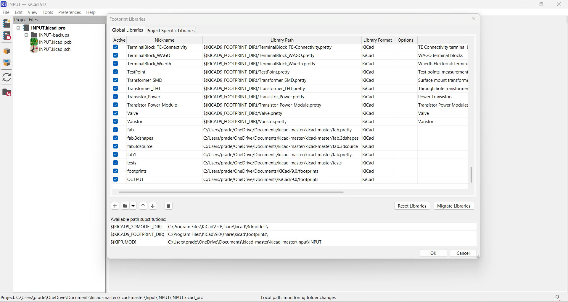
Similarly, I opened the "Manage Footprint Libraries" option and imported the previously created mod file so I could use the custom shape in my PCB layout.
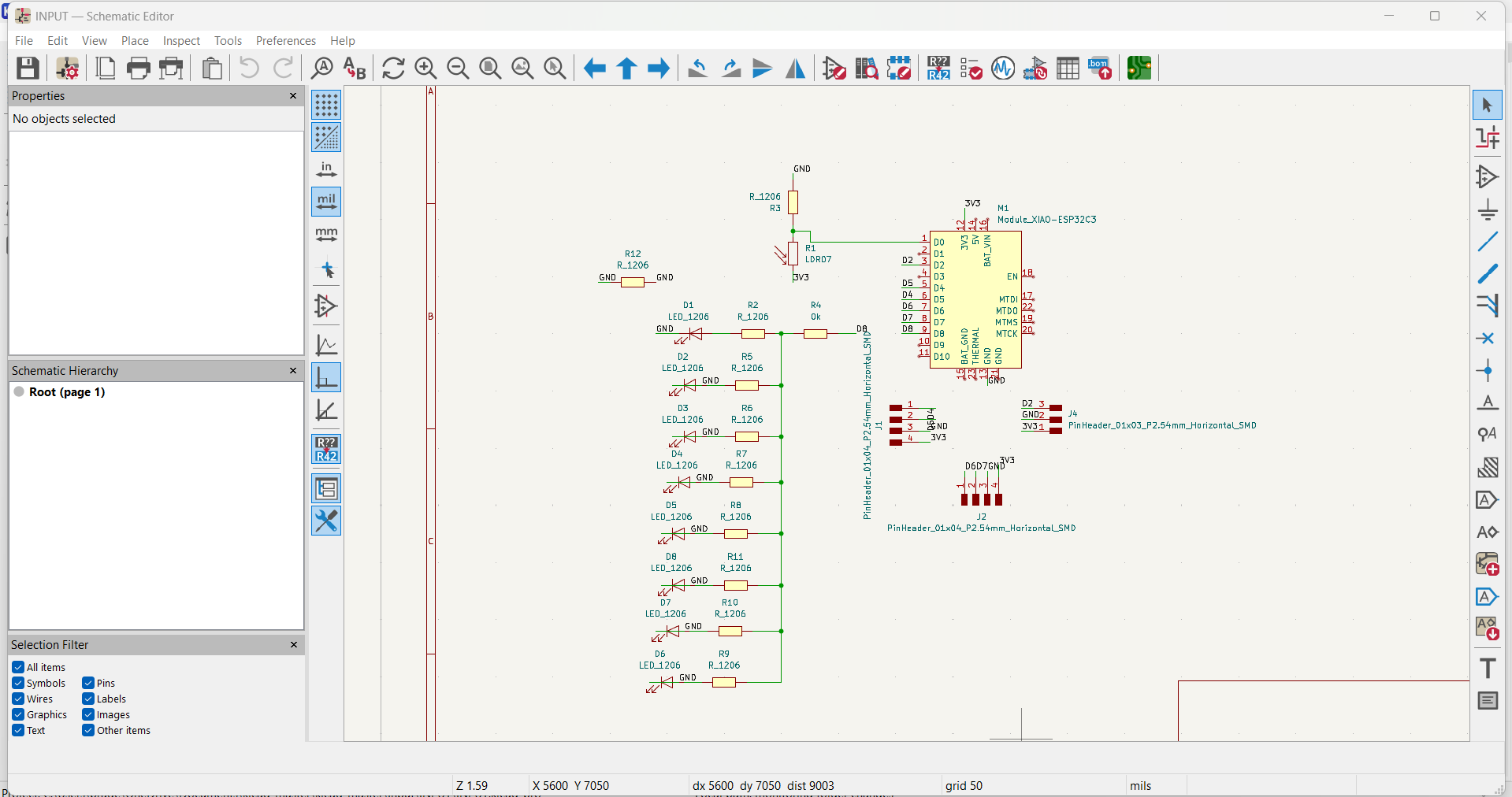
Once the libraries were added, I started designing the schematic by placing all necessary components based on the circuit requirements.
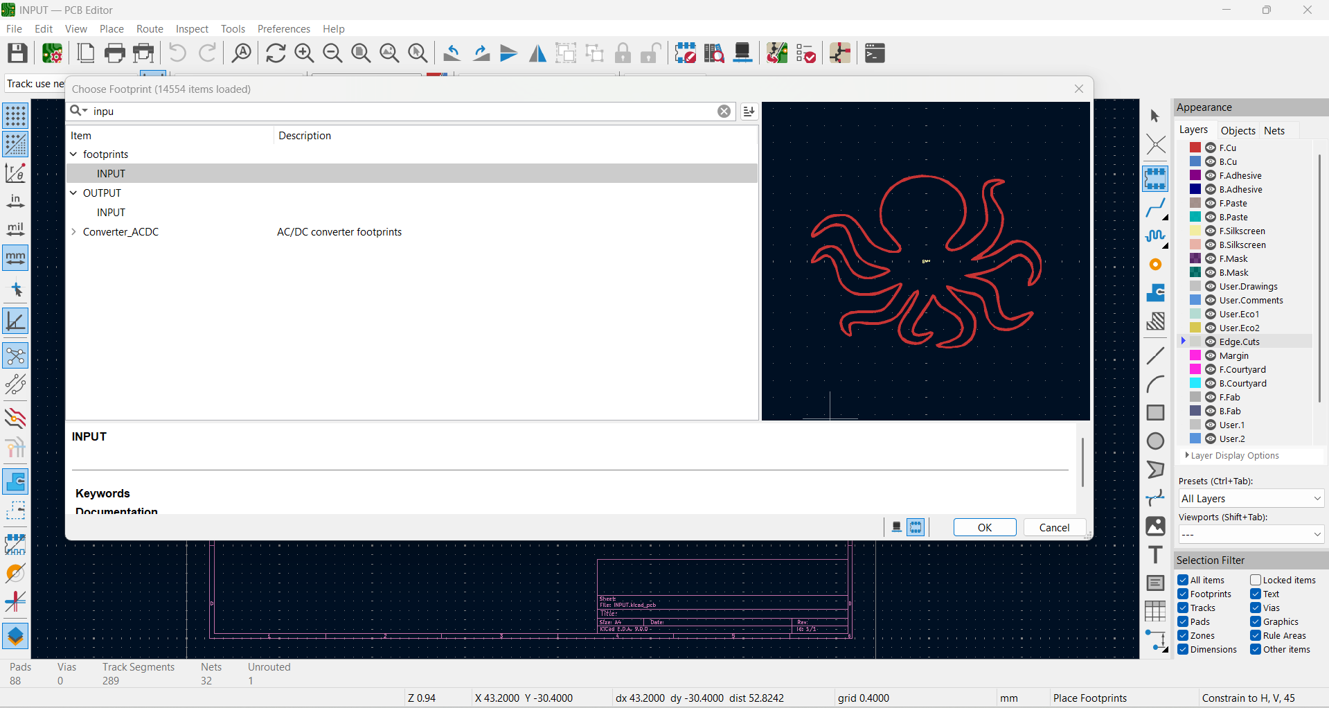
Using the "Place Footprint" tool, I selected each component and assigned the appropriate footprint. When I clicked "Choose Footprint," the symbol appeared, and I matched it with the corresponding component name.
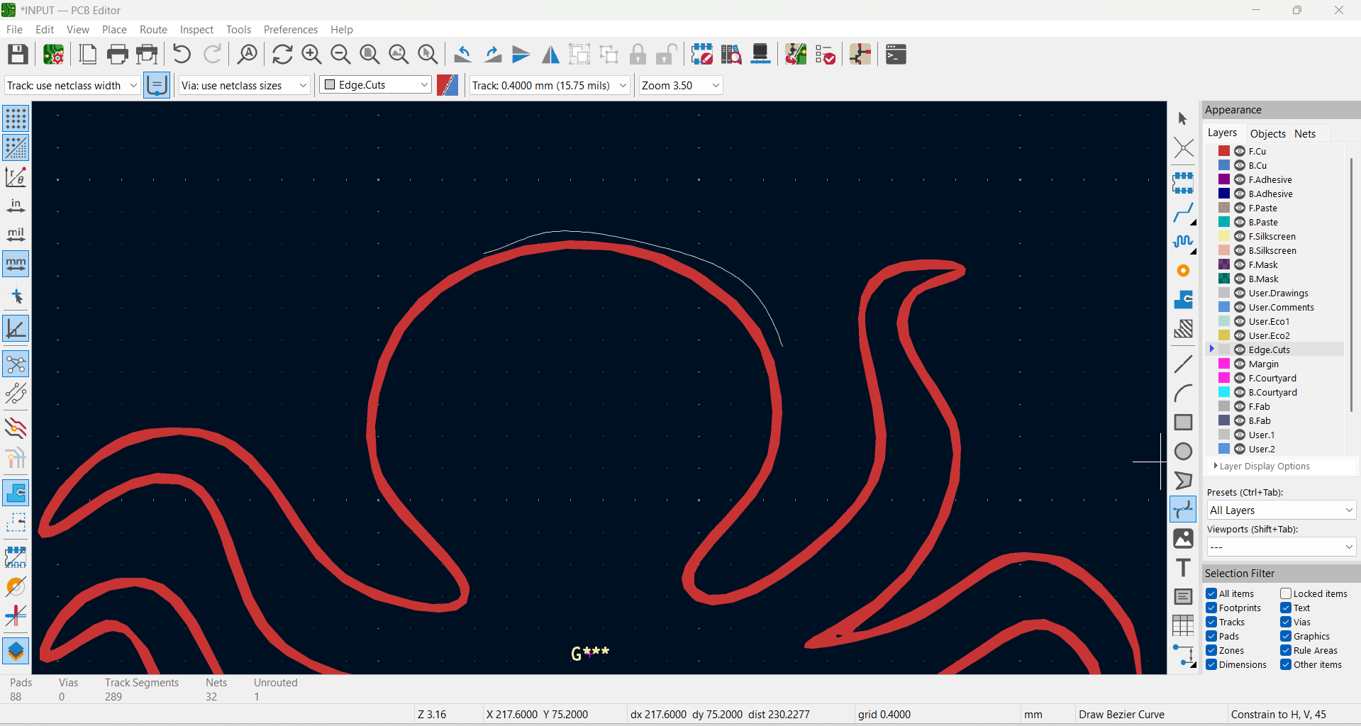
To finalize the board shape, I drew an edge cut line around the octopus outline, ensuring that the PCB followed the same shape. After defining the edges, I removed the temporary image file used for reference.
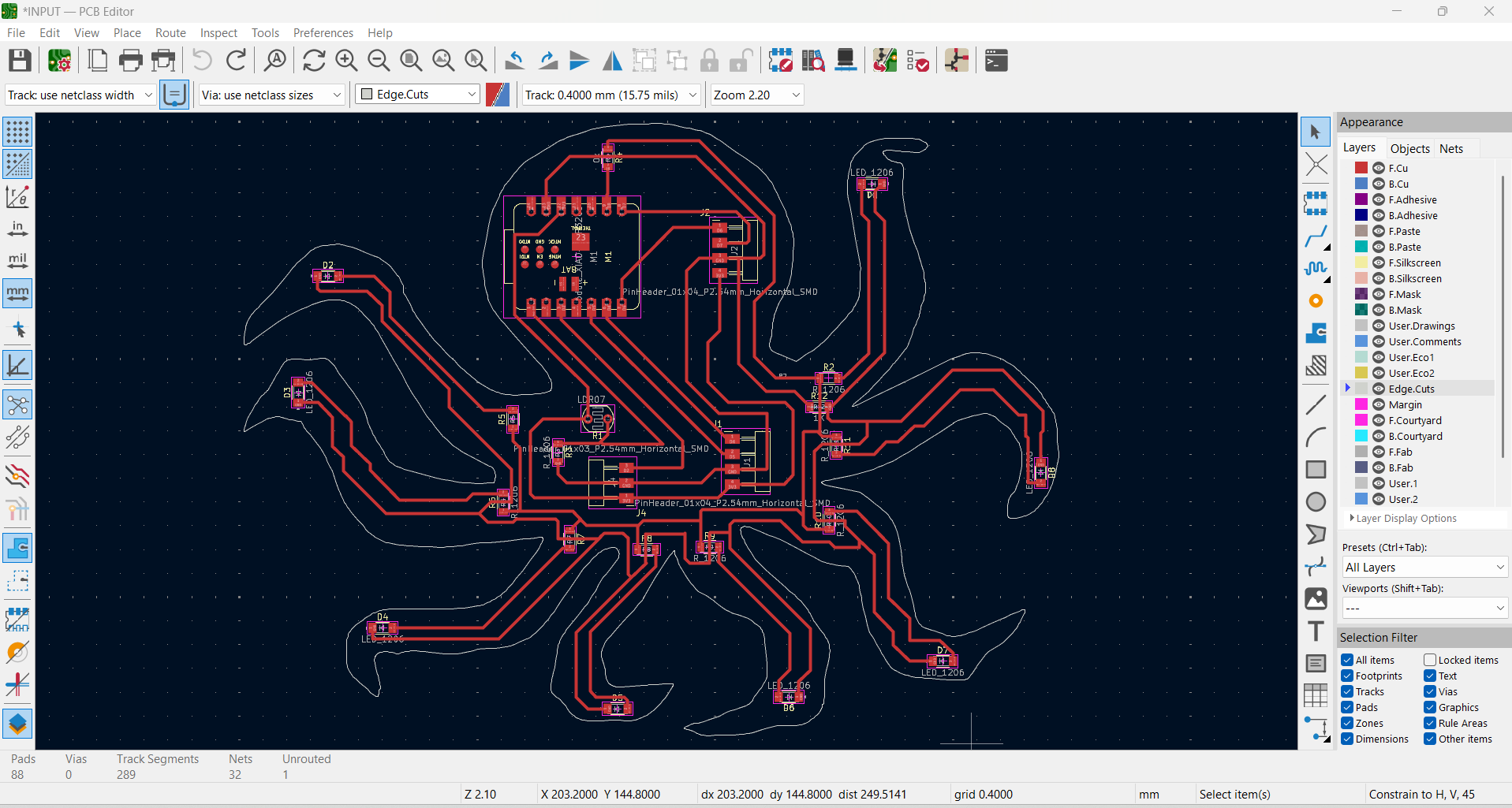
I completed the routing process by connecting all components with appropriate traces, ensuring a functional and efficient layout.
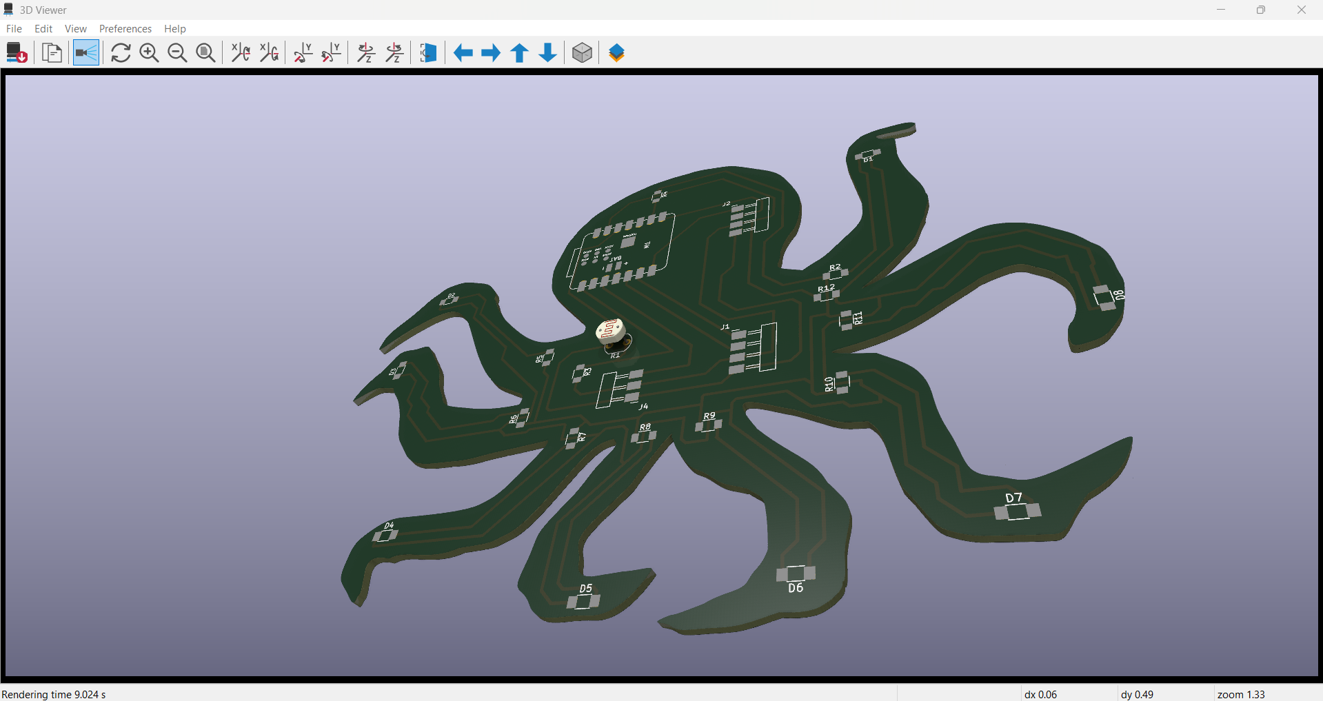
Finally, I previewed the 3D model of my octopus-shaped PCB and exported the file for fabrication.
Converting Gerber File to PNG Format
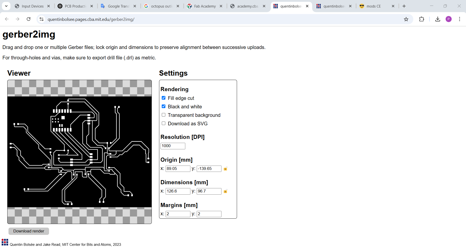
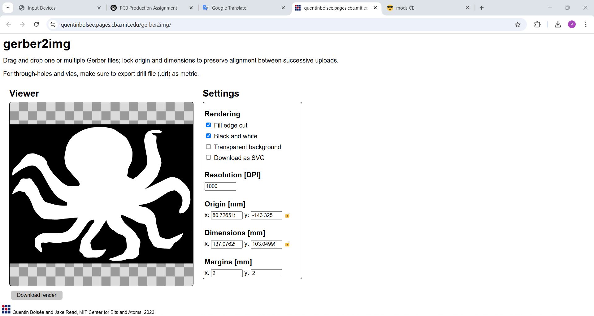
To convert my Gerber file into a PNG image, I accessed the Gerber2Image (Gerber2IMG) website from my home computer.
I uploaded the Gerber file on the platform, and it successfully generated a downloadable PNG version of my design.
If you're interested in learning the detailed step-by-step process, please refer to my documentation for the Electronics Production assignment.
G-code Generation Using Mods
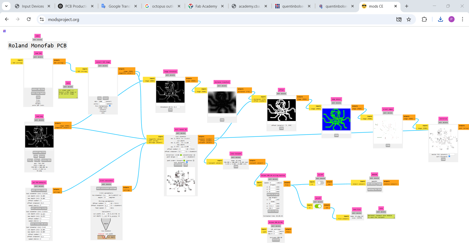
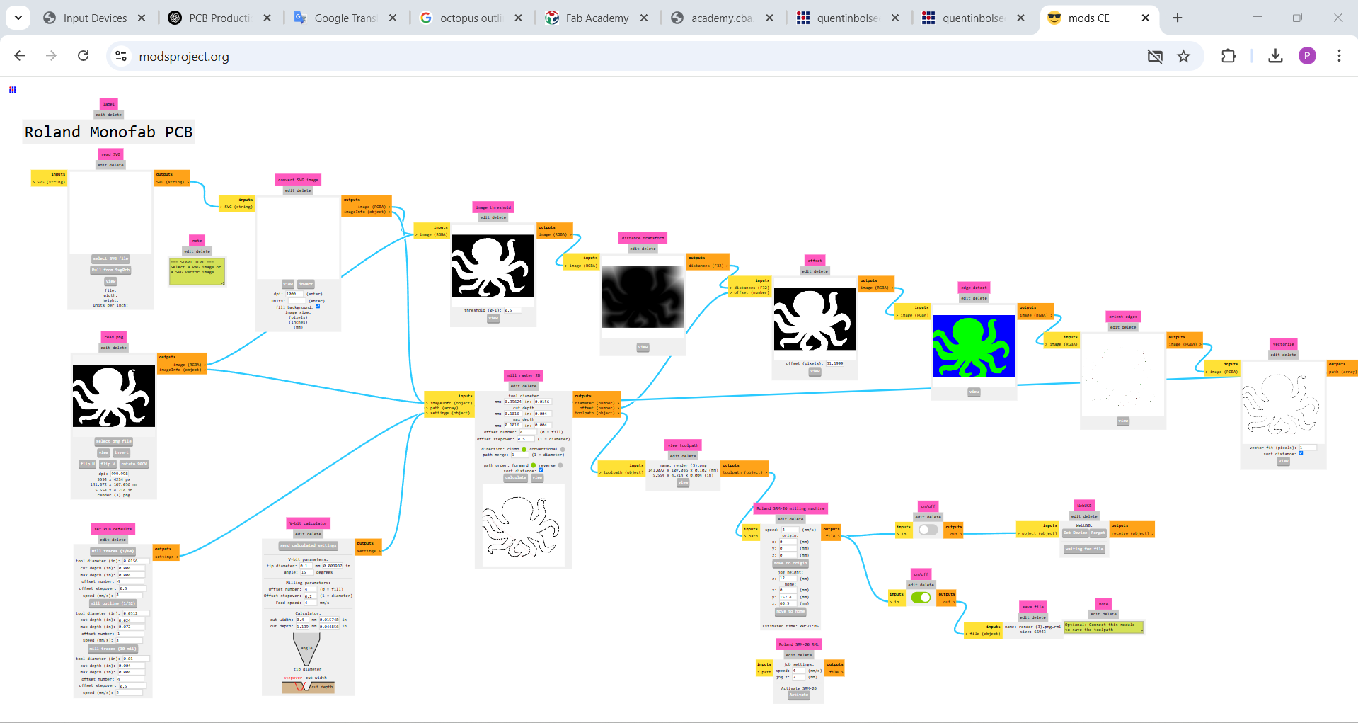
I used the Mods software to successfully generate G-code for both the internal and external outlines of my PCB design. This tool allowed me to precisely control the toolpaths and ensure the accuracy of the final milling process.
To explore the complete step-by-step procedure I followed, please refer to my Electronic Production assignment.
PCB Cutting Process
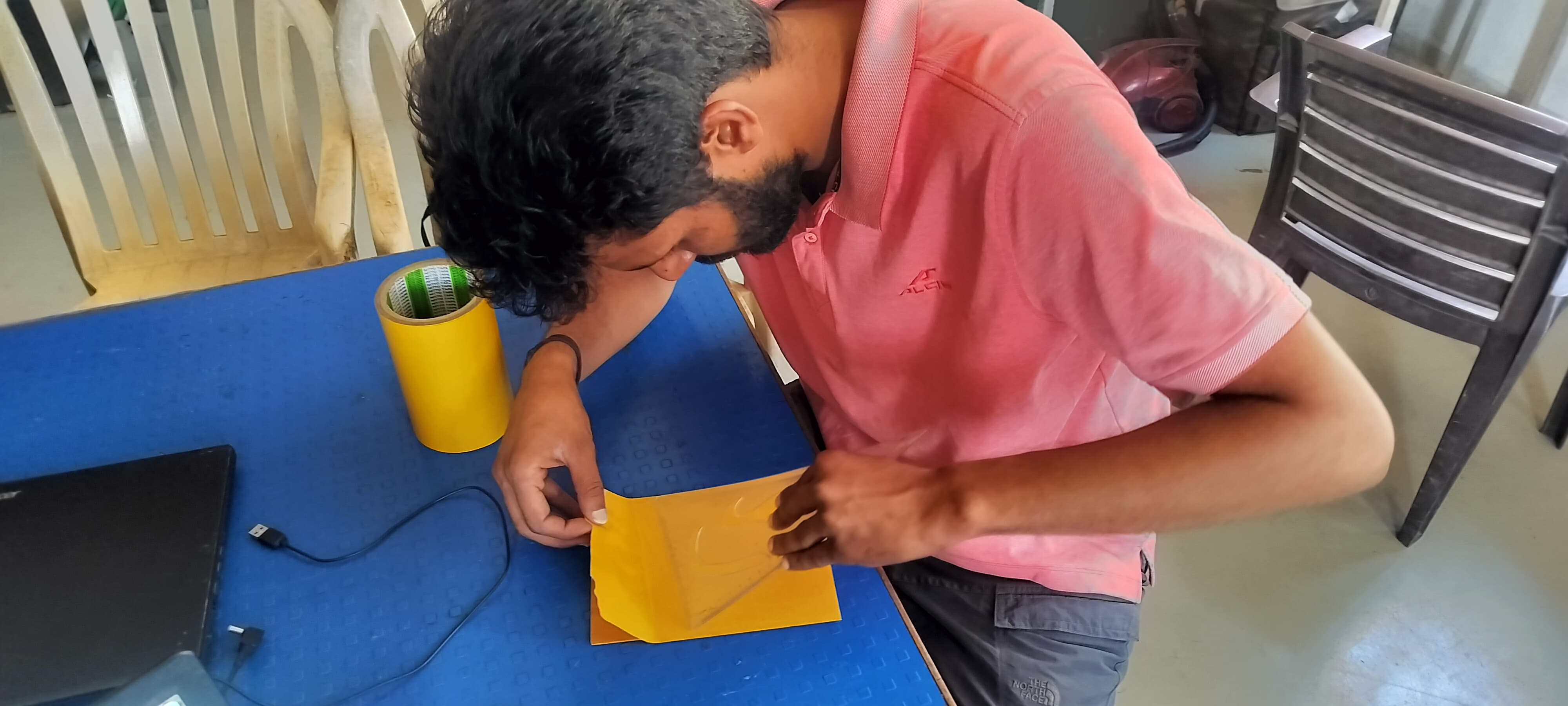
To begin the process, I carefully applied double-sided tape on the PCB board based on the required dimensions. This ensured that the board was firmly attached to the machine bed before initiating the milling process.
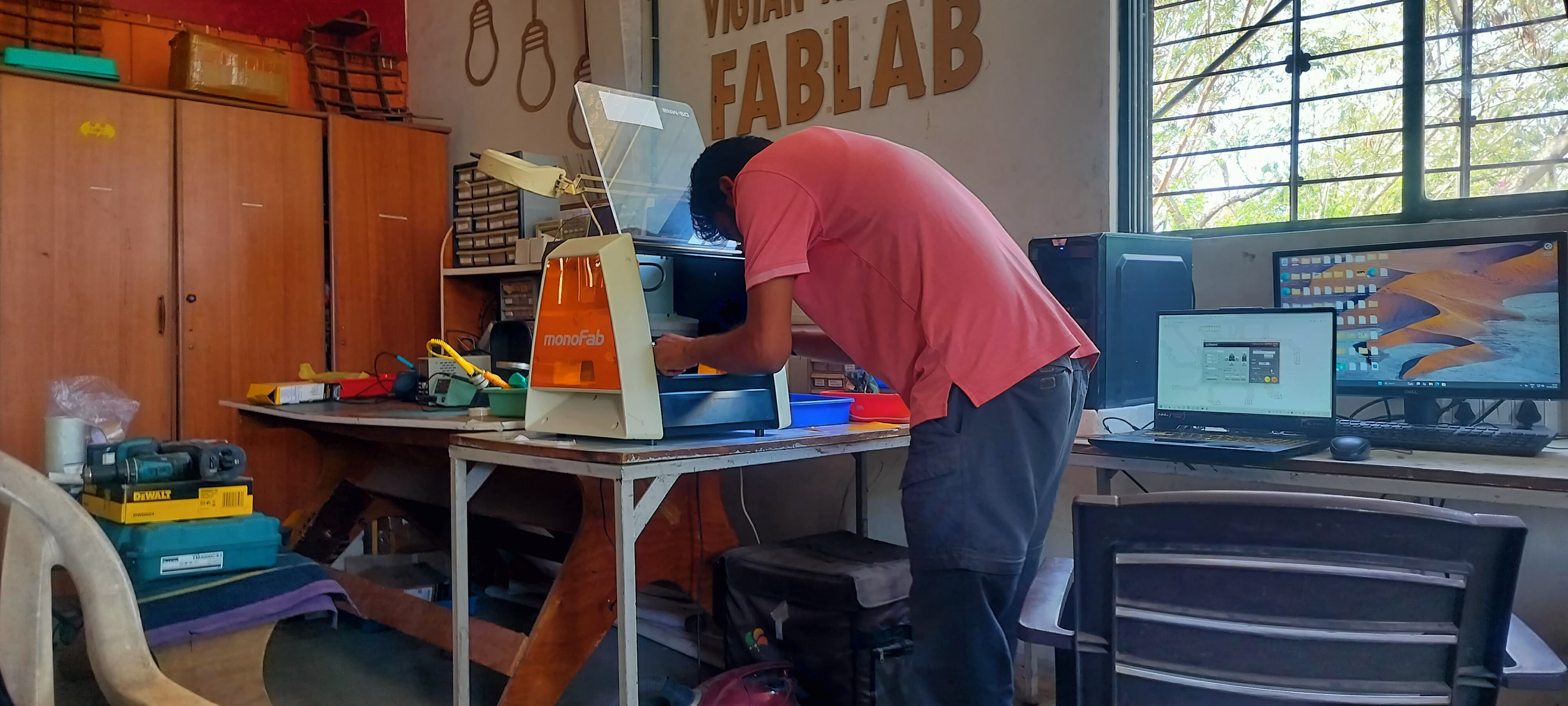
Next, I accurately positioned the PCB onto the SRM-20 milling machine bed, aligning it correctly to avoid any displacement during the cutting operation.
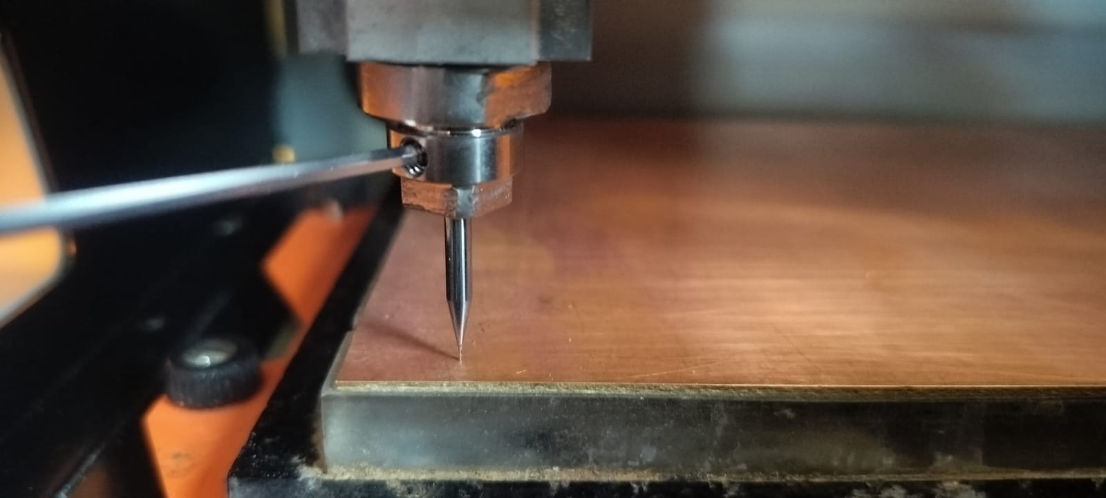
After securing the board, I installed the end mill bit into the spindle of the SRM-20, making sure it was tightly fixed for precise cutting.
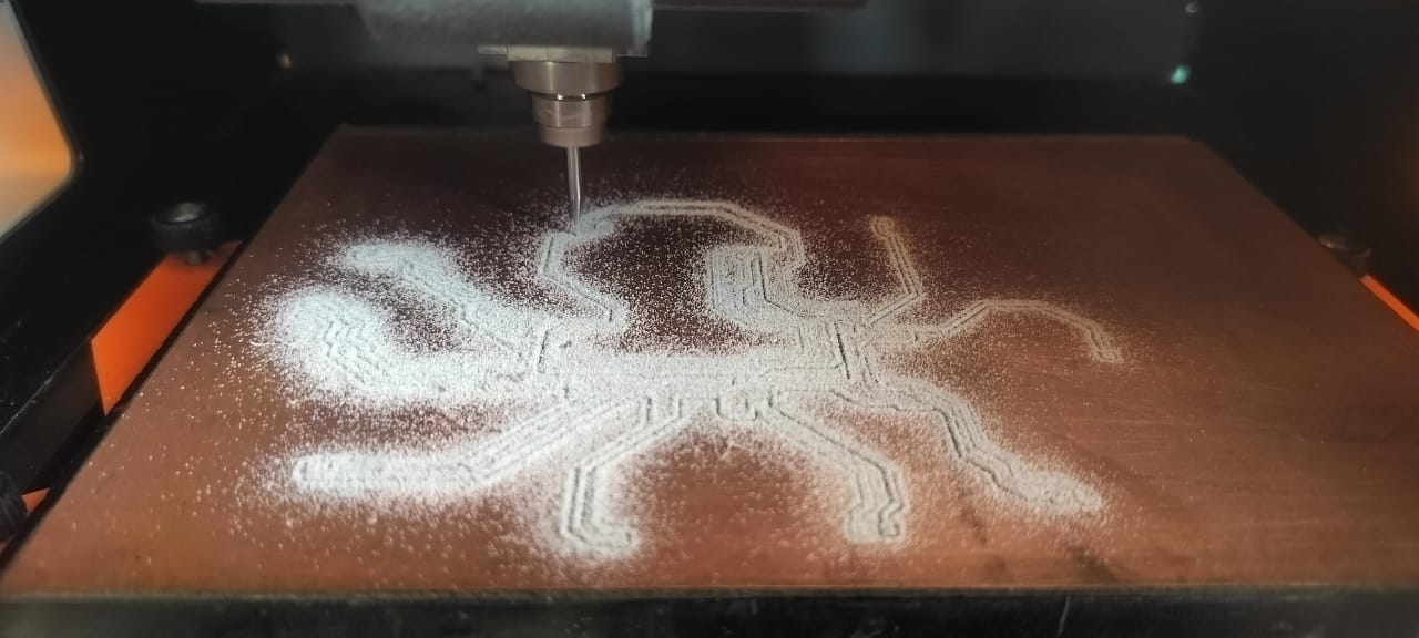
Once everything was set up, I uploaded and executed the G-code file that contained my PCB design. The machine then started the cutting process based on the provided paths.
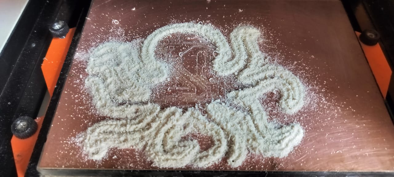
Upon successful execution of the command, the PCB cutting was completed accurately as per the design specifications.
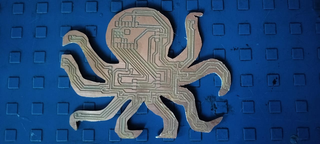
Finally, I carefully removed the PCB from the machine bed and cleaned it to remove any dust or remaining debris.
To explore the entire process in more detail, please visit my Electronic Production assignment page.
Soldering Process
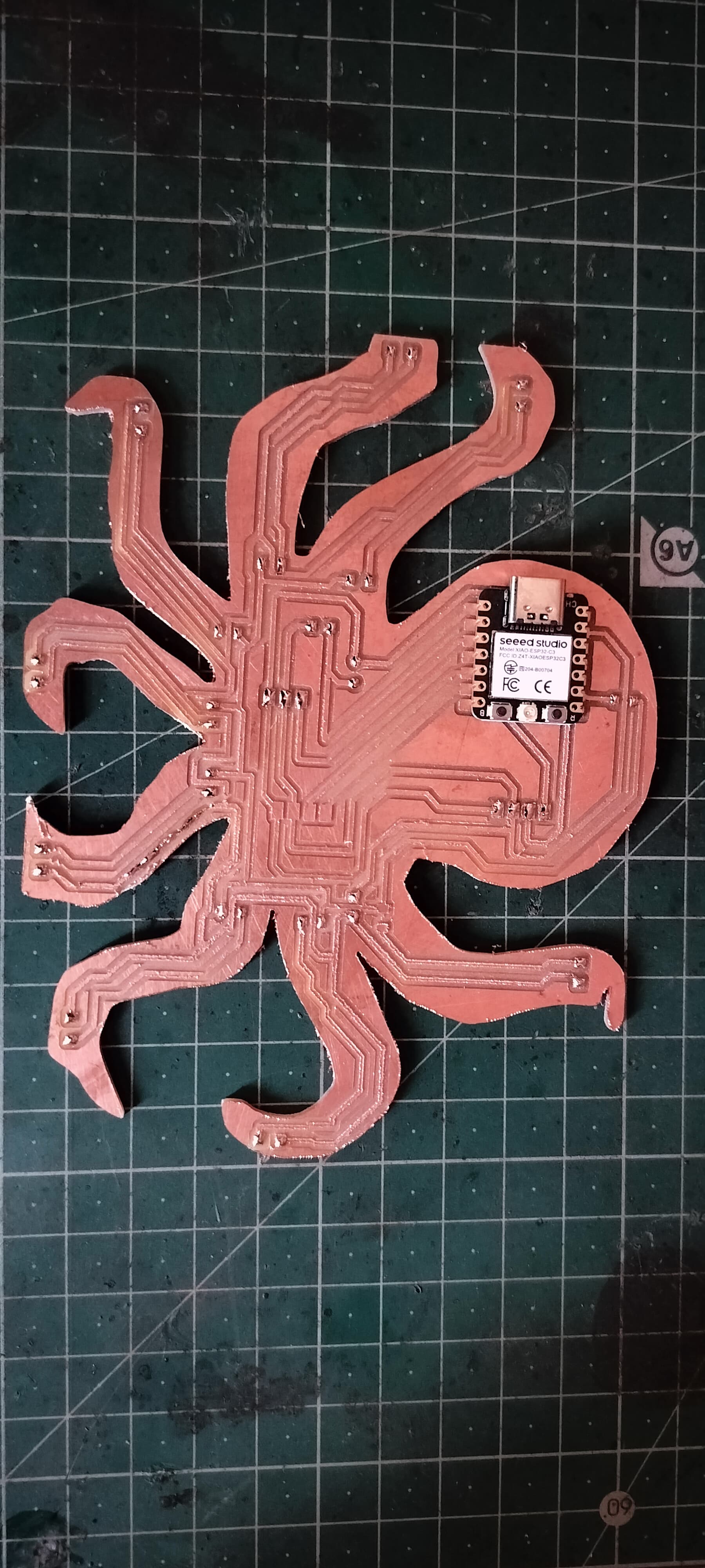
The following components were used to assemble the PCB:
- 1 × XIAO ESP32-C3 microcontroller
- 2 × 4-pin connectors
- 1 × 3-pin connector
- 8 × LEDs
- 8 × 4.99KΩ (4990 ohm) resistors
- 2 × 0Ω resistors
- 1 × LDR (Light Dependent Resistor)
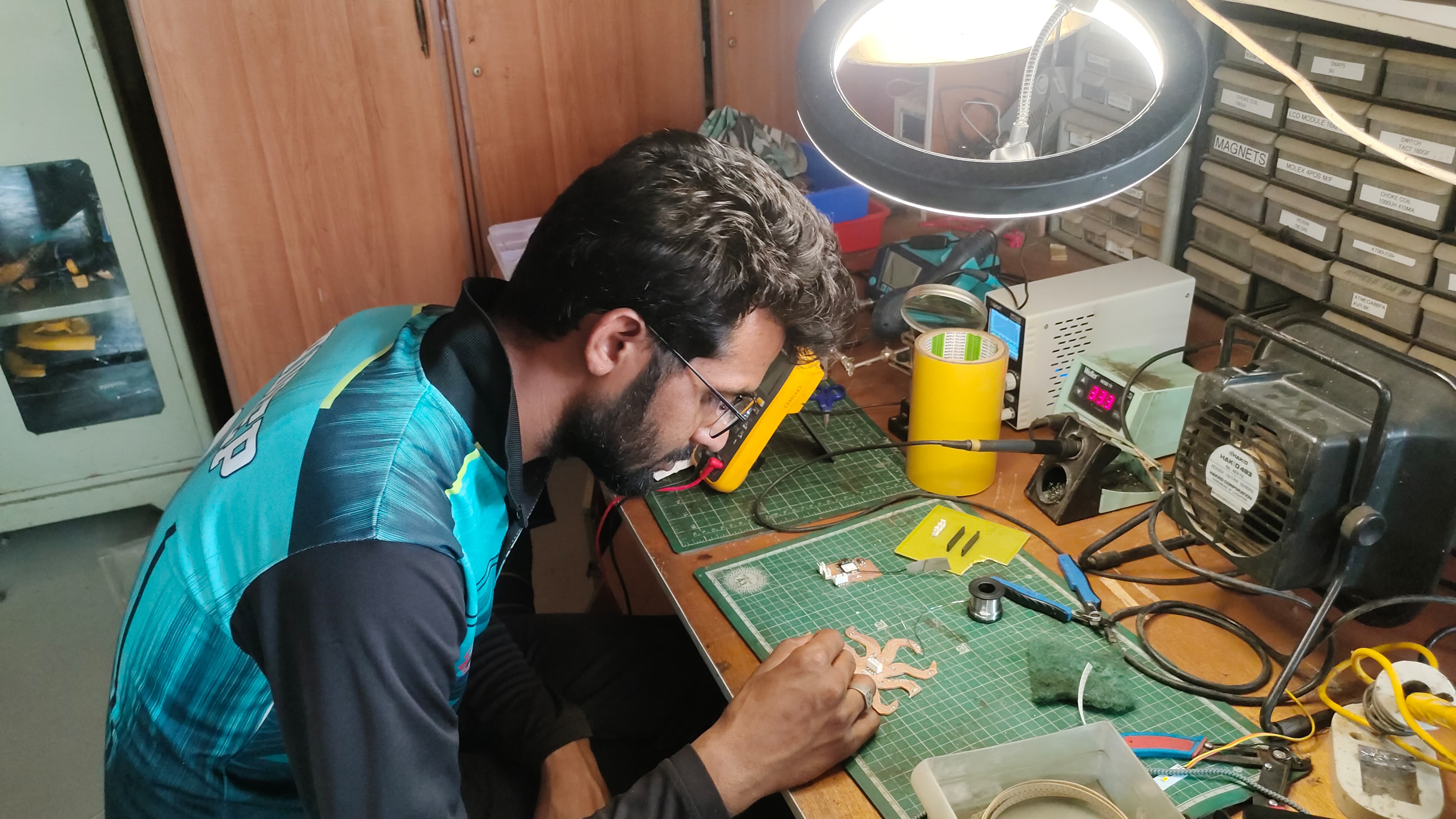
I began the soldering process by preparing all the necessary components and ensuring the PCB was clean and ready for assembly.
The first component I soldered onto the board was the microcontroller IC, which required precision and careful alignment with the pads.
After the IC was secured, I continued by soldering one LED, a corresponding resistor, a 3-pin connector, and one of the 4-pin connectors.
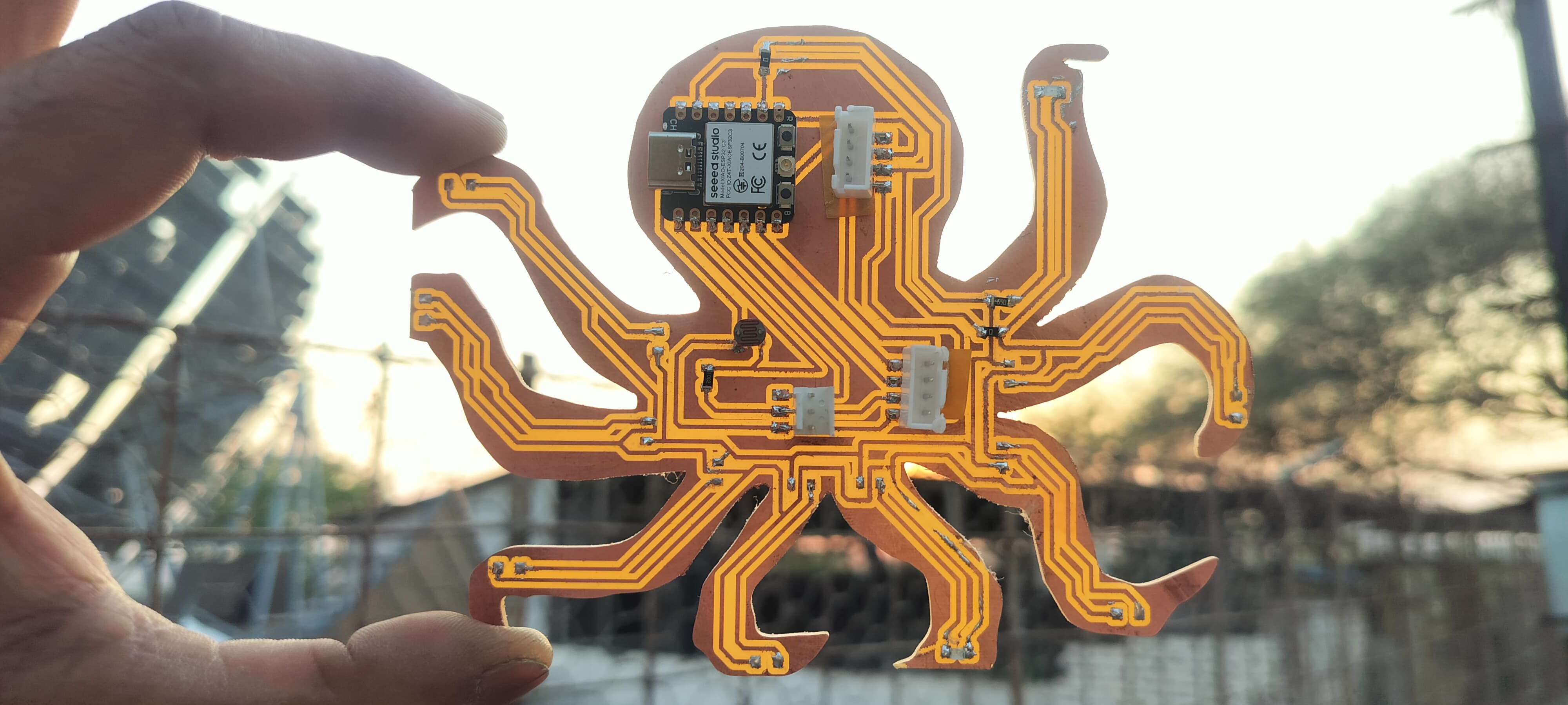
Once the key components were in place, I tested the continuity across all soldered points using a multimeter to ensure proper connectivity. I also tested the LED to confirm that the board was functioning as expected.
After successfully testing the basic functionality, I proceeded to solder the remaining LEDs and resistors onto the board.
With all components now soldered, my microcontroller board is fully assembled and ready for programming and further testing.
Programming and Testing Process
To begin, I launched the Arduino IDE and uploaded the code onto the board.
Code:
#define LDR_PIN A0   // LDR connected to A0 (Analog)
#define LED_PIN 8    // LED connected to D8

void setup() {
    pinMode(LED_PIN, OUTPUT);
    Serial.begin(115200);
}

void loop() {
    int ldrValue = analogRead(LDR_PIN);
    Serial.print("LDR Value: ");
    Serial.println(ldrValue);

    if (ldrValue < 1500) {
        digitalWrite(LED_PIN, HIGH);
        Serial.println("Dark Detected - LED ON");
    } else {
        digitalWrite(LED_PIN, LOW);
        Serial.println("Light Detected - LED OFF");
    }

    delay(500);
}
Reference: ChatGPT
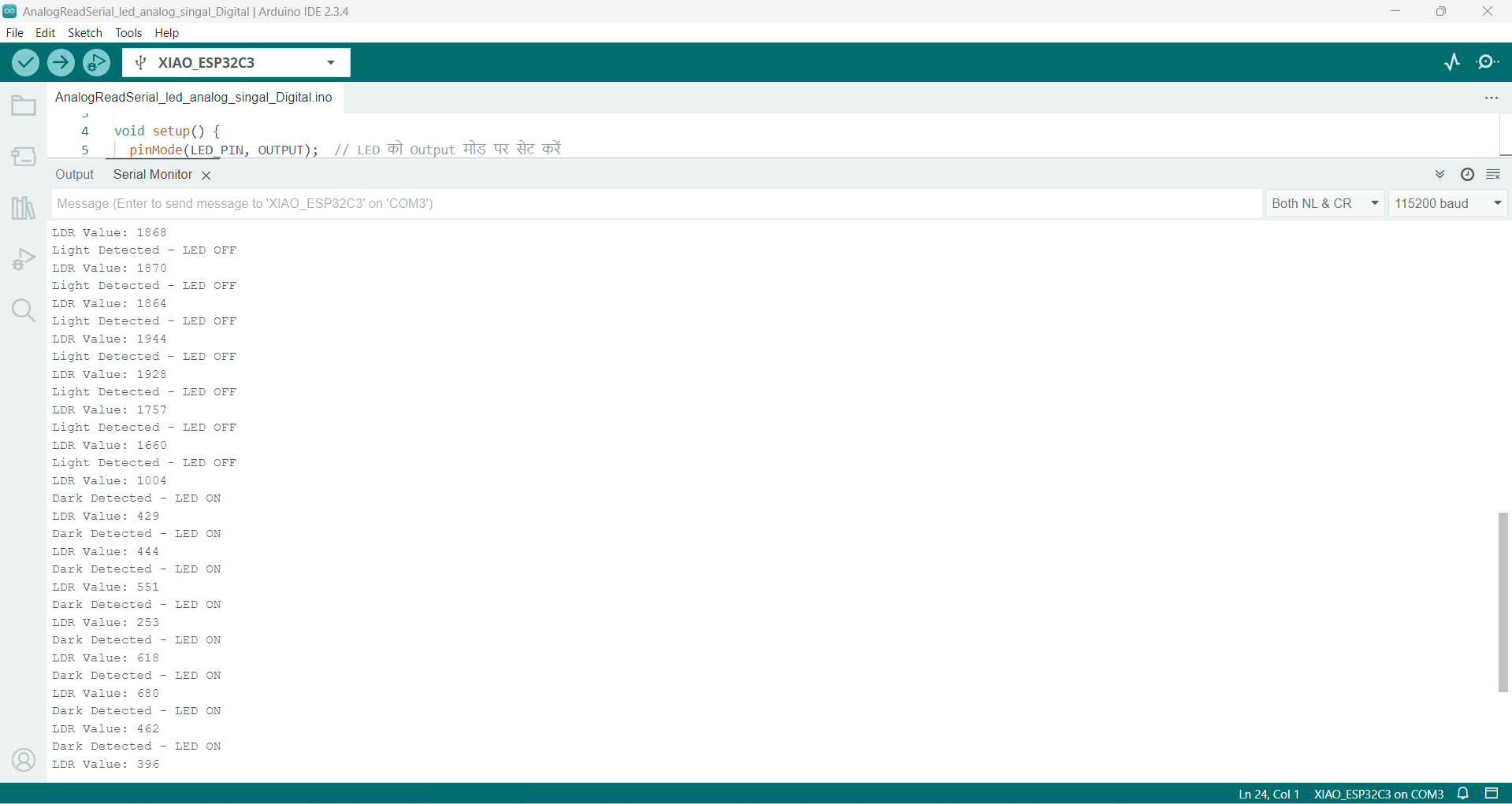
Next, I checked the serial monitor to verify if the LDR sensor and the LED were functioning properly. The results confirmed that everything was working as expected.
LED Blinking with LDR Sensor: When the light is turned on, the LED turns off, and when the light is switched off, the LED turns on. This behavior was successfully detected by the LDR sensor, as per the logic implemented in the code.