Week 6
Assignment: Electronics Design
Group assignment
The Link of Group assignments.
Individual assignment
- use an EDA tool to design a development board that uses parts from the inventory to interact
- and communicate with an embedded microcontroller
- extra credit: try another design workflow
- extra credit: simulate your design
- extra credit: design a case around your design
Introduction
This assignment marks my first experience working with an Electronic Design Automation (EDA) tool. For my PCB design journey, I selected KiCad, an open-source software widely used for schematic capture and PCB layout design.
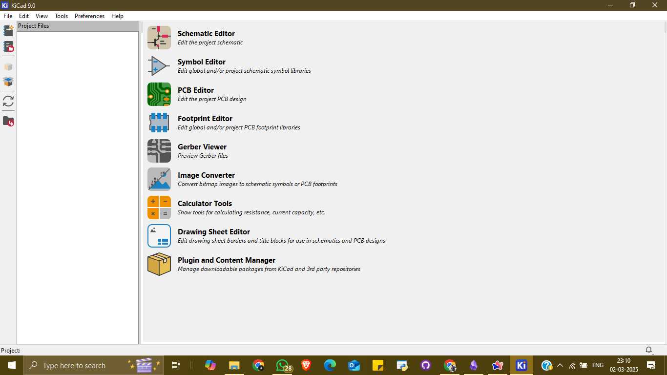
Downloading and Exploring KiCad :
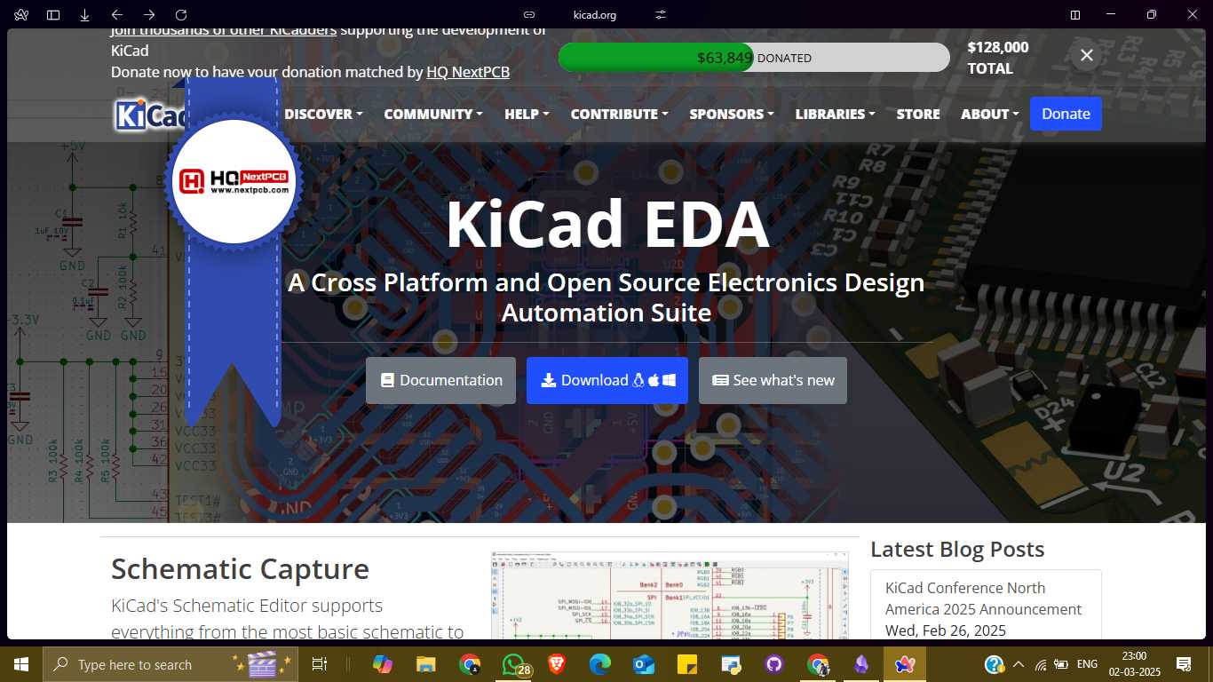
The first step was to download KiCad from its official website. The software provides detailed documentation and tutorials on how to handle schematic design and PCB layout, making it an excellent choice for beginners. The official KiCad website offers structured learning resources, which I found useful while getting started.
Schematic Diagrams :
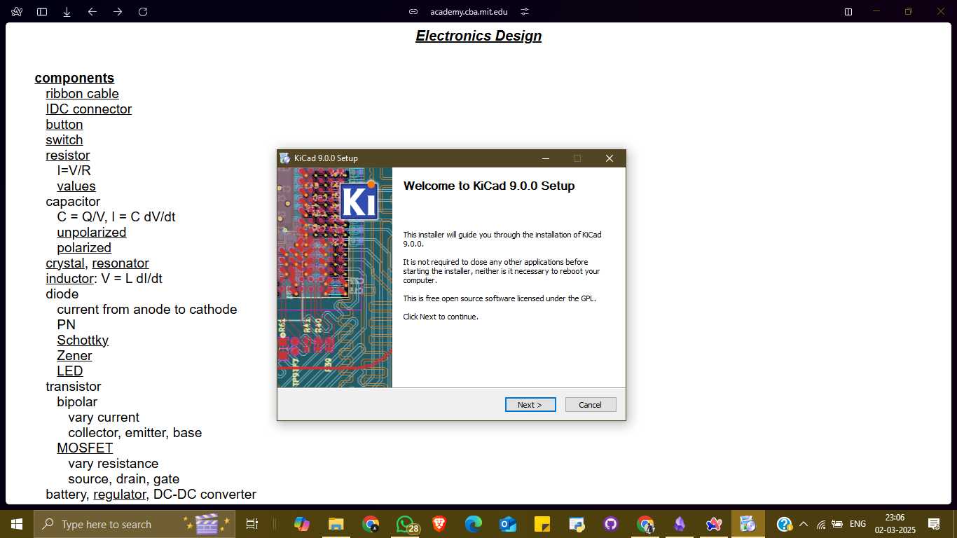
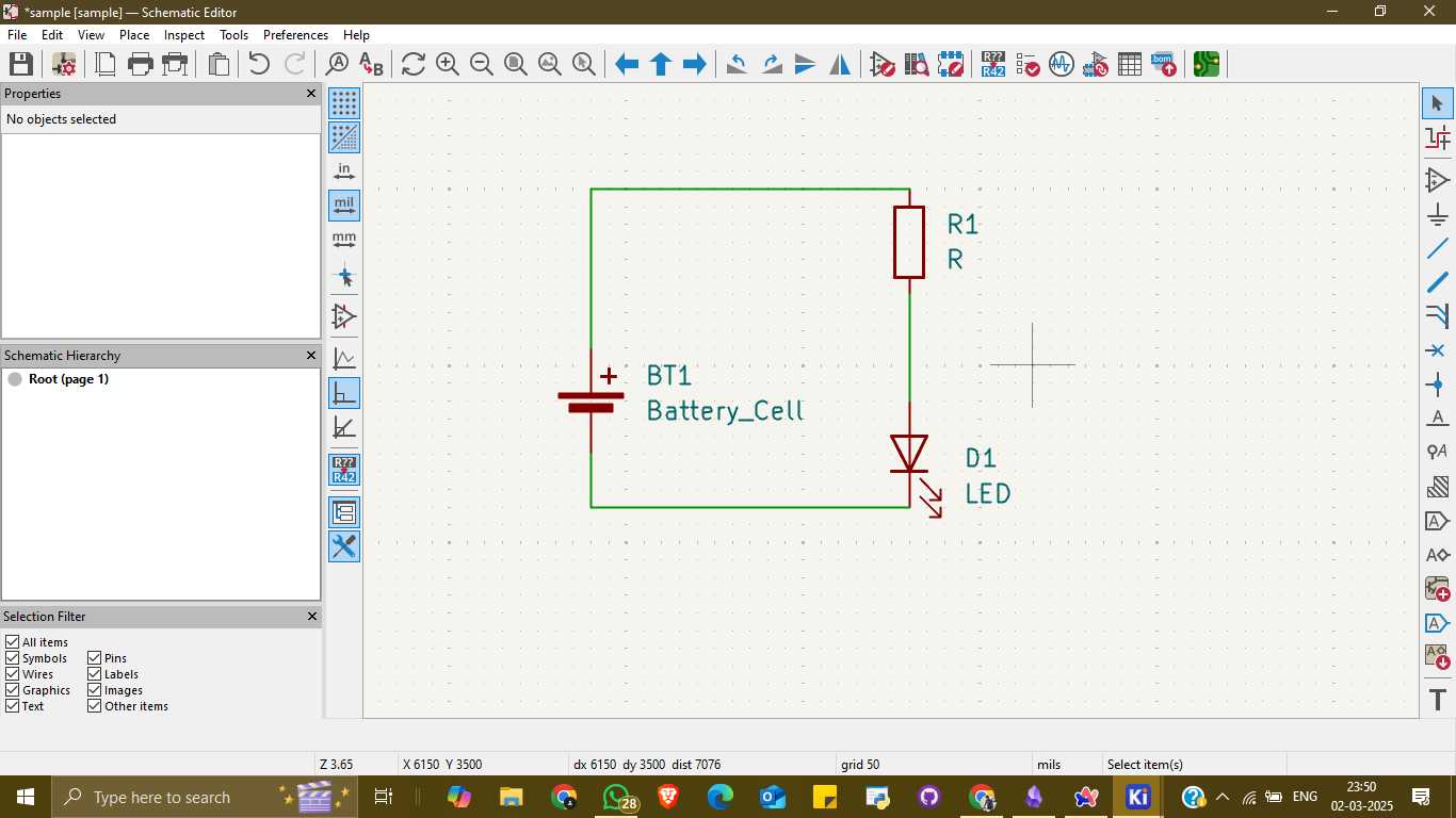
Since I had never worked with an EDA tool before, I referred to multiple tutorials to understand how to read schematic diagrams. To get comfortable with KiCad's workflow, I worked through the example files available on the KiCad learning page. This helped me understand the step-by-step design process, which includes:
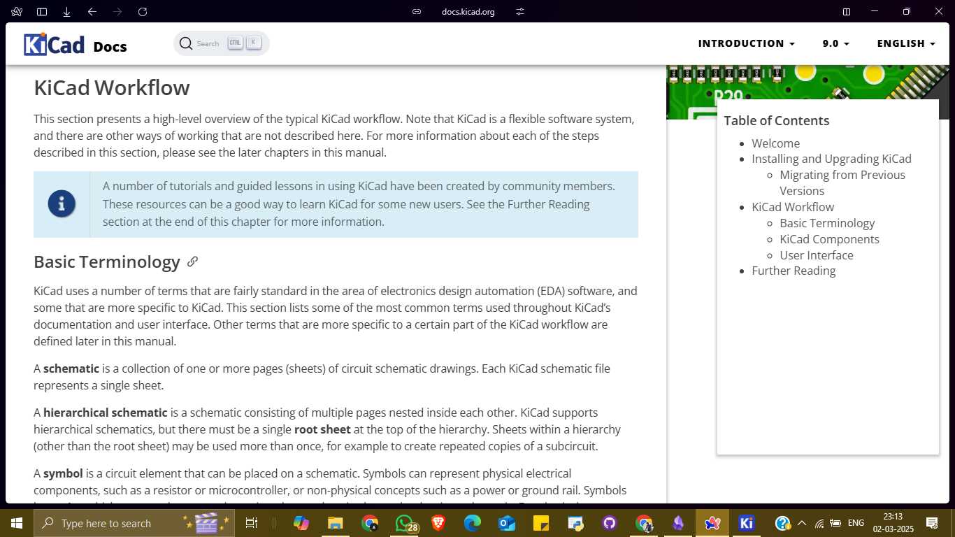
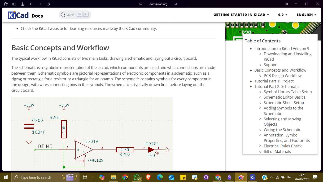

KiCad Workflow :
- 1. Creating the Schematic Diagram - Drawing the circuit diagram using symbols for different components.
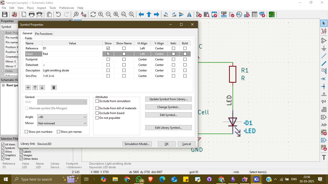
- 2. Assigning Component Values - Specifying values for resistors, capacitors, and other elements.
- 3. Assigning Footprints - Selecting the physical package for each component.
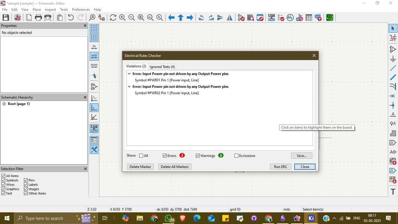
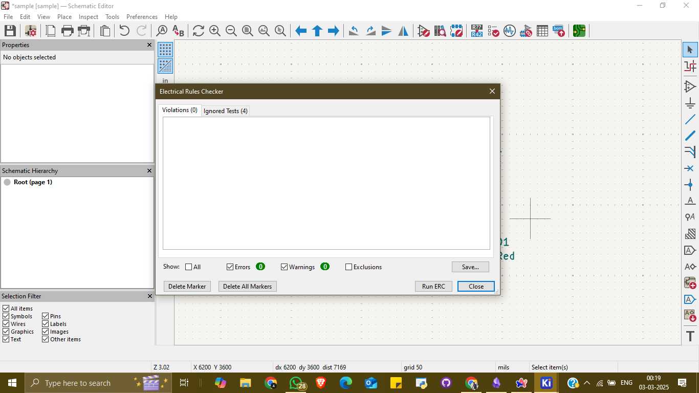
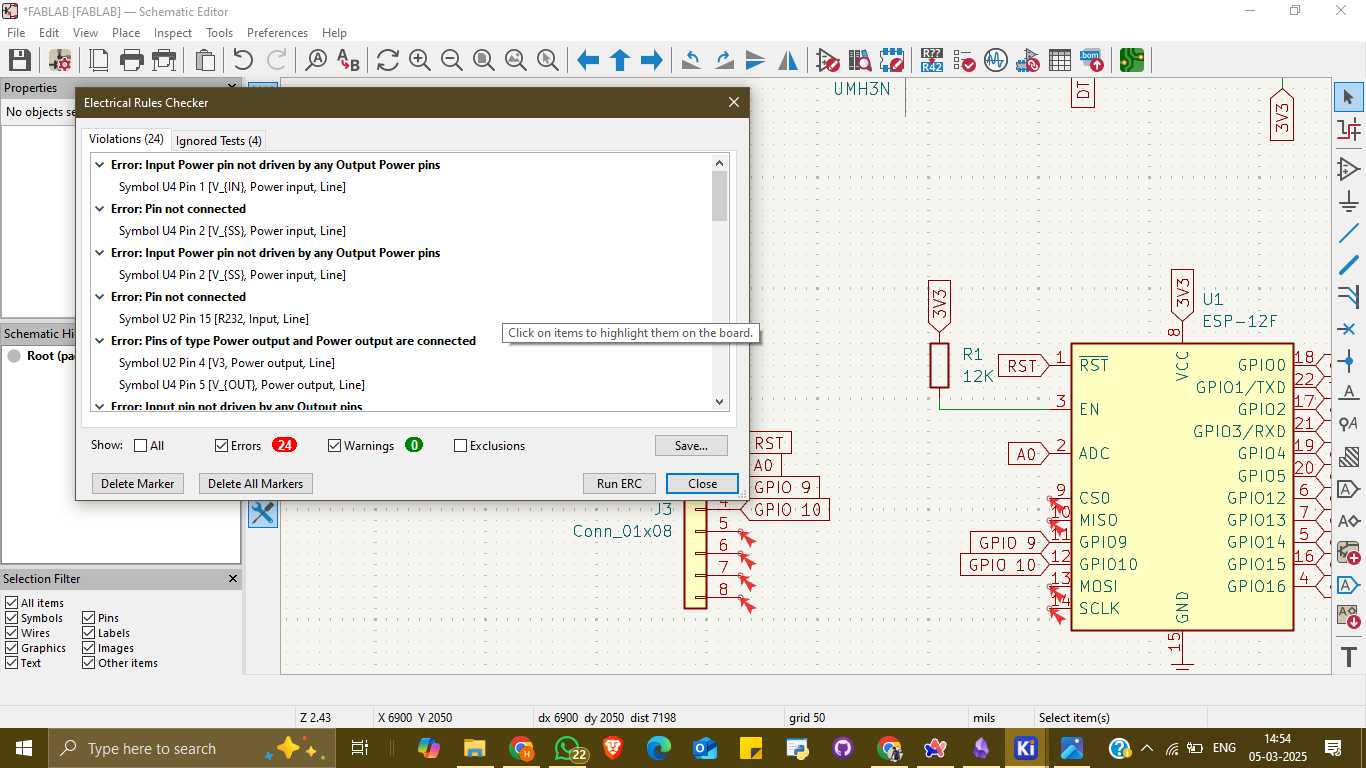
- 4. Running the Electrical Rules Check (ERC) - Identifying and resolving electrical connection errors.
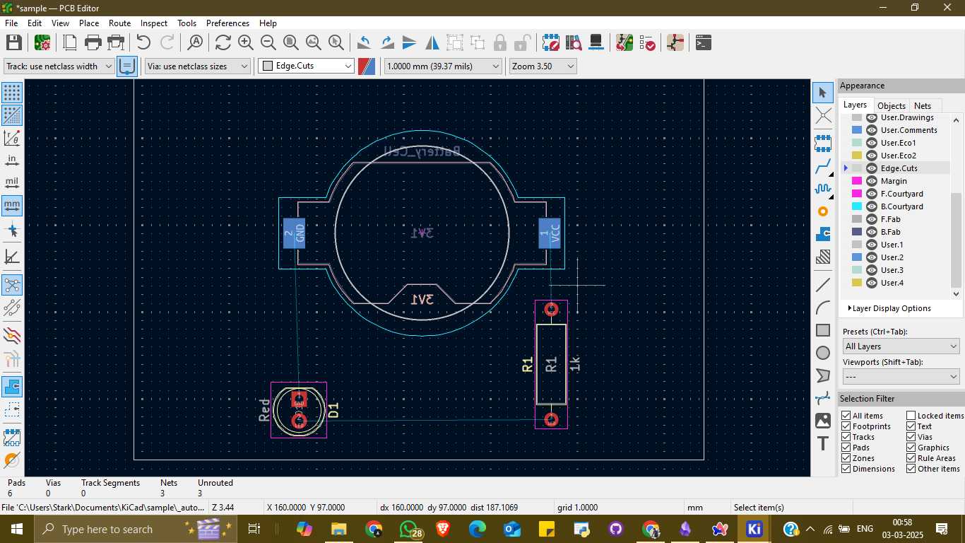
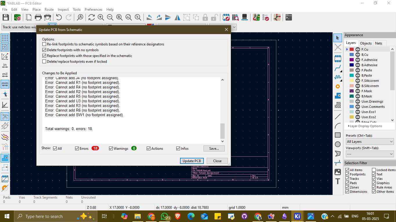
- 5. Converting the Schematic to PCB Layout - Transferring the schematic into the PCB editor.
- 6. Placing Components and Routing Traces - Ensuring an optimal layout for signal flow and power distribution.
- 7. Running the Design Rule Check (DRC) - Validating trace widths, clearances, and manufacturing constraints.
- 8. Generating a 3D Render View - Visualizing the final board before exporting for fabrication.

Project Inspiration :
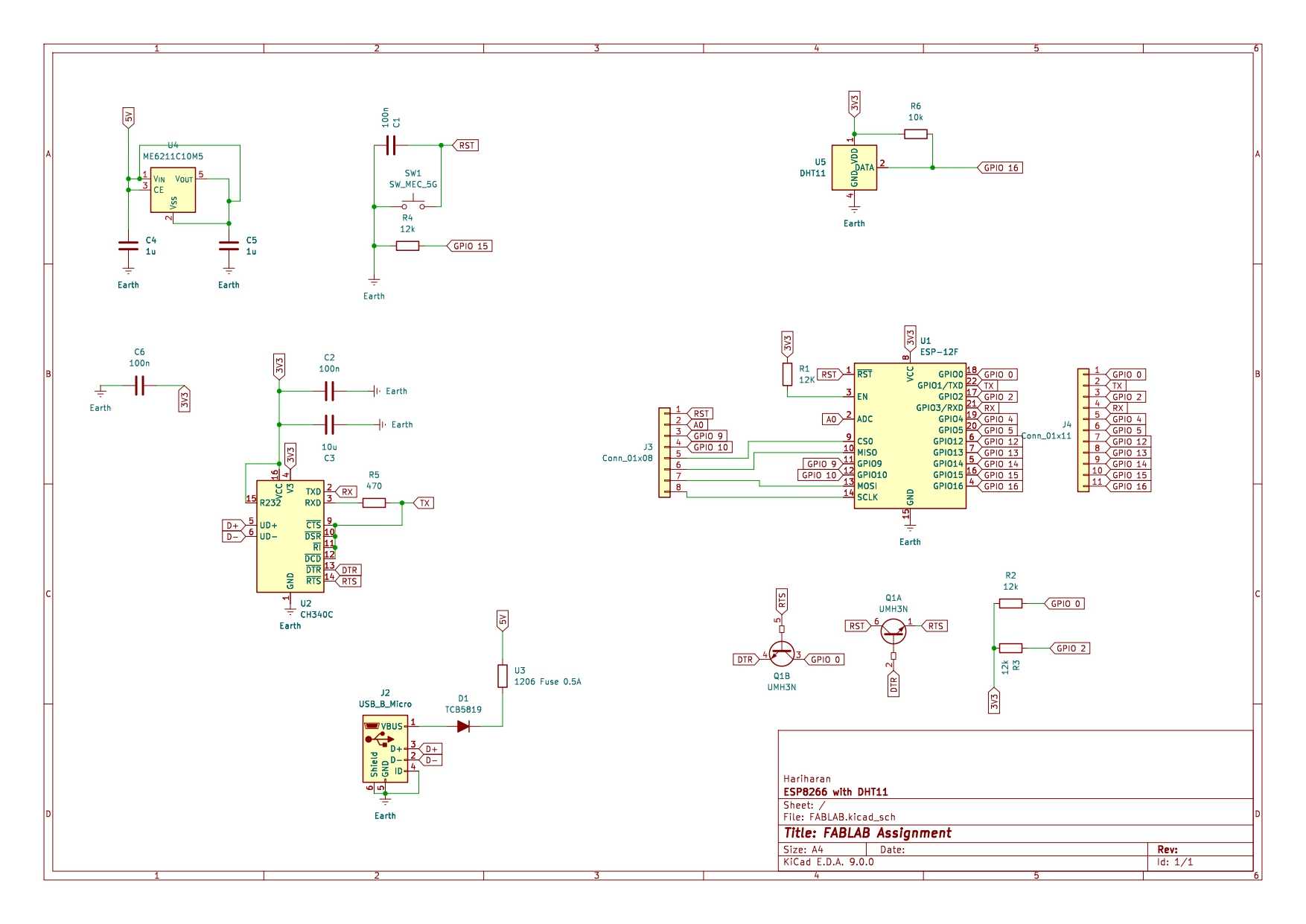
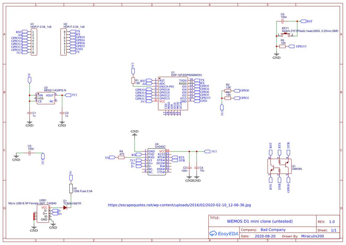
For my first project, I wanted to design a Temperature & Humidity Sensor Board that integrates an ESP8266 microcontroller and a DHT11 sensor. I was inspired by existing projects that combine these two components into a single PCB for data collection and wireless communication.
- 1. Collecting Schematic References: I searched for open-source schematic designs for the ESP8266 and DHT11.
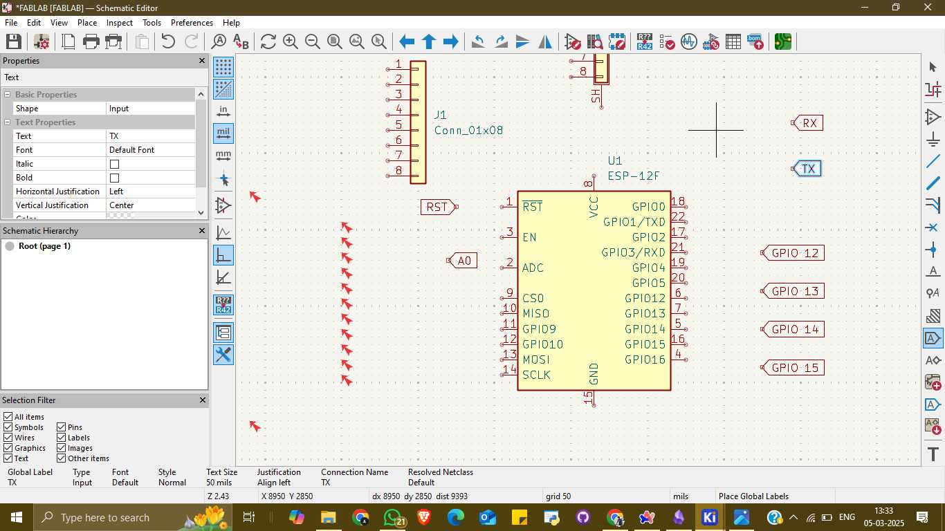
- 2. Creating the Schematic in KiCad: I drew the circuit in KiCad on a single-page schematic file, ensuring all connections were correctly placed.
- 3. Running ERC: I conducted the Electrical Rules Check (ERC) and cleared all errors
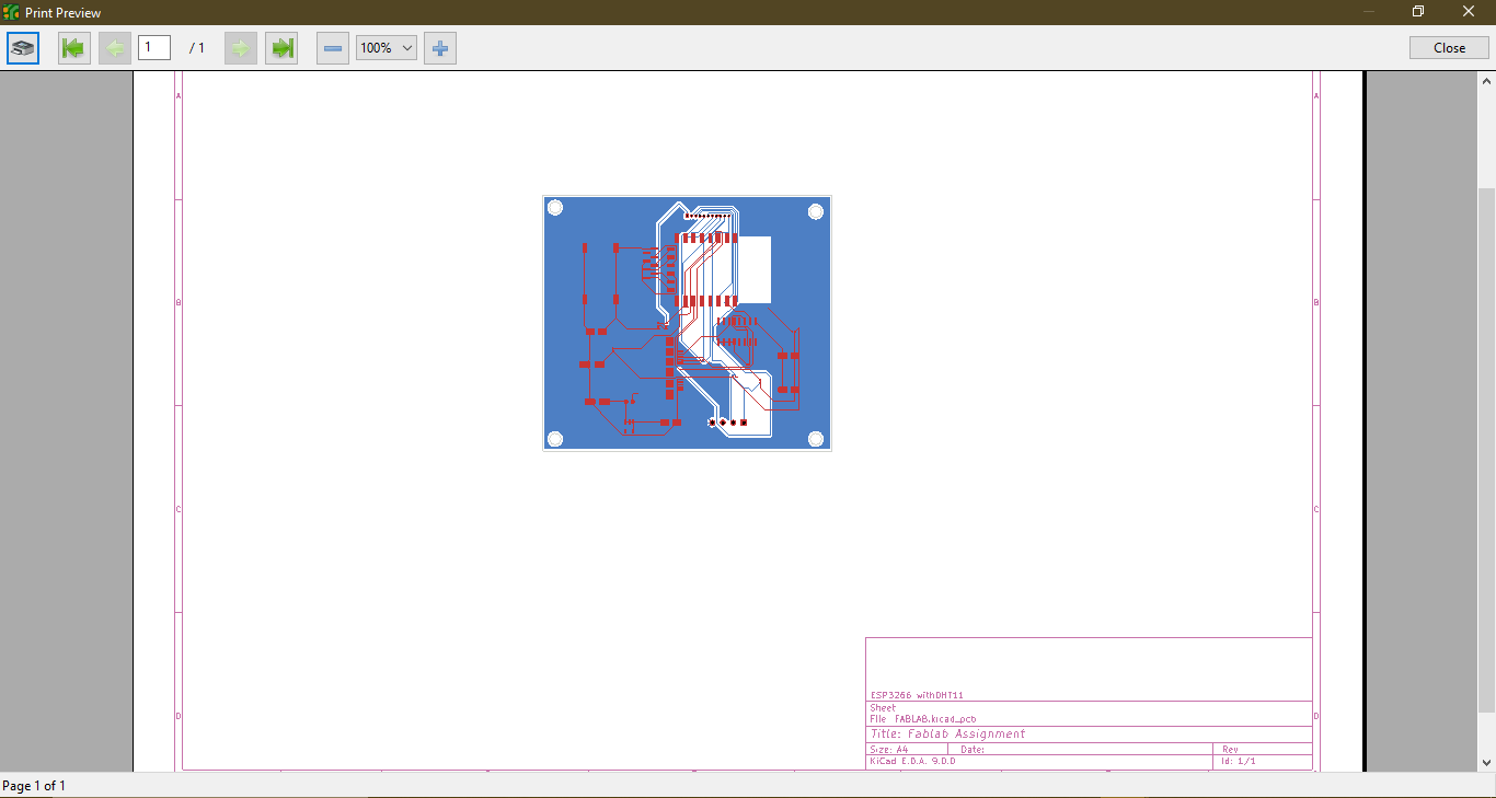
- 4. Converting to PCB Layout: After validating the schematic, I transferred it to the PCB editor.
- 5. Performing DRC Check: I verified trace widths, spacing, and other design rules to ensure manufacturability.
- 6. 3D Render View: Finally, I used KiCad's 3D viewer to visualize my design before exporting it for manufacturing.
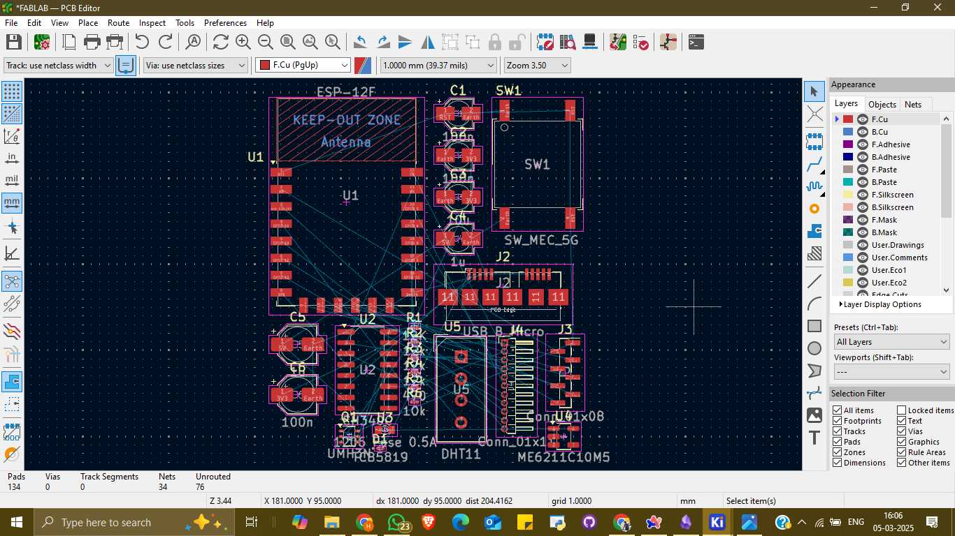

Conclusion :
Through this assignment, I gained hands-on experience with KiCad, learning how to design a PCB from start to finish. The step-by-step workflow allowed me to understand schematic design, PCB layout, and the essential verification processes. This project has given me confidence in working with EDA tools, and I look forward to developing more complex designs in the future.
