Individual Assignment: Make and Test a Microcontroller Development Board
1. Define Project Requirements
Question:
Determine the specific functionalities your development board should support, such as processing power, memory capacity, input/output interfaces, and communication protocols.
Answer:
The answer given here is a continuation from week 6 which was about electronic design of a development board. The schematic and the pcb was achived in KiCad.
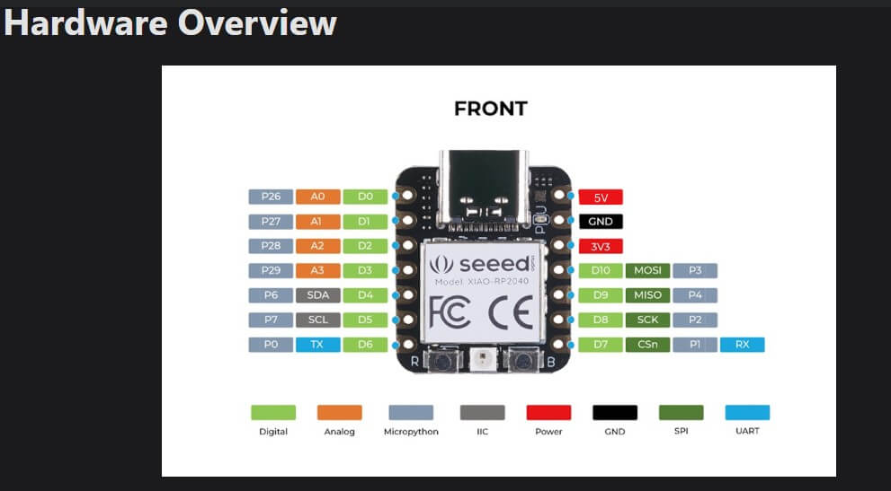
The XIAO RP2040 microcontroller development board supports the following functionalities:
Processing Power: The RP2040 has a dual-core Arm Cortex-M0+ processor running at 133 MHz, sufficient for small to medium-scale embedded projects like sensor interfacing or IoT applications.
Memory Capacity: The RP2040 includes 264 KB of SRAM and 2 MB of flash memory on the XIAO RP2040, adequate for small programs and data storage in hobbyist projects.
Input/Output Interfaces: The board provides 11 digital I/O pins, 4 analog inputs (ADC), and includes:
Pin headers (J5, J2, J3, J4) for GPIO access to connect sensors or actuators.
A push-button (SW1, "SWITCH_TACTILE_OMRON") for user input, such as reset.
An LED for status indication, connected to a GPIO pin via resistors R1 and R2.
Communication Protocols: The RP2040 supports:
UART (J3 header labeled "UART").
SPI (J4 header labeled "SPI").
I2C (J2 header labeled "I2C").
These enable communication with peripherals like sensors or displays. The board is designed for general-purpose prototyping in educational or experimental settings.
Click the link below to view the data sheet of the SEED XIAO-RP2040
Choose a microcontroller that aligns with your project needs. Consider factors like architecture, clock speed, available peripherals, power consumption, and package type.
Answer:
The XIAO RP2040 aligns with the project needs based on the following:
Architecture: The RP2040 uses a dual-core Arm Cortex-M0+ 32-bit architecture, balancing performance and power efficiency for embedded applications.
Clock Speed: The RP2040 runs at 133 MHz, sufficient for real-time tasks like sensor data processing.
Available Peripherals: The RP2040 provides:
30 GPIO pins (11 accessible on the XIAO RP2040).
2 UART, 2 SPI, and 2 I2C controllers (accessible via J3, J4, J2 headers).
4 ADC channels for analog input.
16 PWM channels for motor or LED control.
Power Consumption: The RP2040 consumes 20-30 mA in active mode and supports sleep modes, suitable for battery-powered projects.
Package Type: The XIAO RP2040 is a compact module (20 mm x 17.5 mm) with castellated edges, easy to solder onto a PCB.
This microcontroller is ideal for a prototyping development board due to its versatile interfaces, compact size, and sufficient processing power.
3. Design the Schematic
Question:
Create a schematic diagram incorporating the microcontroller and essential components such as power supply circuits, oscillators, reset circuits, and necessary interfaces. Ensure proper decoupling capacitors and include programming headers.
Answer:
XIAO RP2040 designed in KiCAD
The schematic above incorporates the following components:
Microcontroller: The XIAO RP2040 (M1) is the central component, including the RP2040 chip, a 12 MHz crystal oscillator, and 2 MB flash memory.
Power Supply Circuits: The XIAO RP2040 has an onboard regulator converting 5V (via USB-C) to 3.3V. The PCB includes a USB-C connector for 5V input, with VCC and GND traces routed to headers and components.
Oscillators: The XIAO RP2040 has a built-in 12 MHz crystal oscillator, requiring no external oscillator.
Reset Circuits: The PCB includes a tactile switch (SW1, labeled "RESET") connected to the RP2040’s RESET pin for manual resetting.
Necessary Interfaces: The PCB provides headers for:
UART, SPI, and I2C (J3, J4, J2) for external device communication.
Analog pins (J5, labeled "Analog Pins") for ADC inputs.
General-purpose I/O pins via headers on both sides of the XIAO RP2040.
Resistors R1 and R2:
R1 (Connected to the LED D1)
Purpose: Current limiting resistor
Function: It limits the current flowing through the LED to prevent it from burning out.
Typical value: 220–1k ohm depending on LED brightness and supply voltage.
R2 (Connected to the tactile switch SW1):
Purpose: Pull-down resistor
Function: Ensures that the 'RESET' pin is held low (GND) when the switch is not pressed, preventing false triggering due to floating input.
When the button is pressed, the RESET pin gets pulled to VCC, triggering a reset.
Programming Headers: The XIAO RP2040 uses its USB-C port for programming via the RP2040’s USB bootloader, eliminating the need for additional headers.
The design includes essential components and follows best practices for noise filtering and interfacing.
4. PCB Layout Design
Question:
Translate the schematic into a PCB layout, adhering to best practices like keeping trace lengths short, separating analog and digital grounds, and positioning components logically. Perform a Design Rule Check (DRC).
Answer:
XIAO-RP2040 designed in PCB Editor
The PCB layout adheres to best practices:
Trace Lengths: Traces are short, particularly for communication interfaces (UART, SPI, I2C), however the trace for TX is long as the pins are placed separately on either side of the RP2040. Traces from the XIAO RP2040 to headers (J2, J3, J4) are direct, minimizing loops for high-frequency signals like SPI.
Analog and Digital Grounds: The RP2040 uses mostly digital signals. The PCB lacks a separate analog ground plane but has wide ground traces for low-impedance return currents, acceptable for a single-layer board.
Component Positioning: Components are placed logically:
The XIAO RP2040 (M1) is central, with headers (J2, J3, J4, J5) around it for easy access.
The reset switch (SW1) and LED (with resistors R1, R2) are at the bottom, away from high-speed traces to reduce interference.
The USB-C connector aligns with the XIAO RP2040’s USB port at the top.
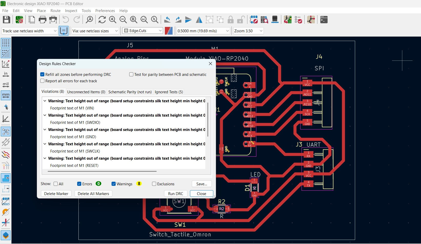
Design Rule Check (DRC):
The layout software reports 0 DRC errors ("Unrouted: 0"), confirming the design meets manufacturing constraints.
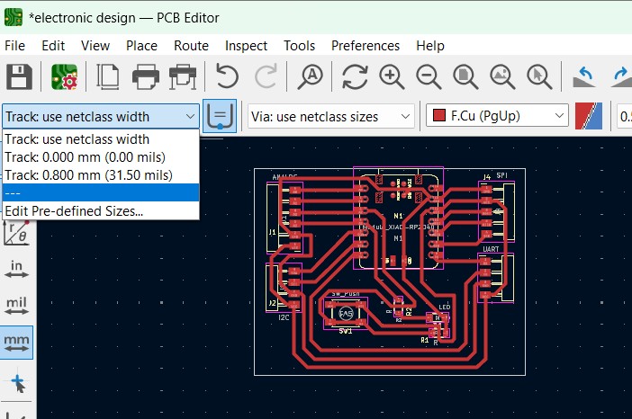
The track width (0.800 mm) ensures manufacturability for a single-layer board.
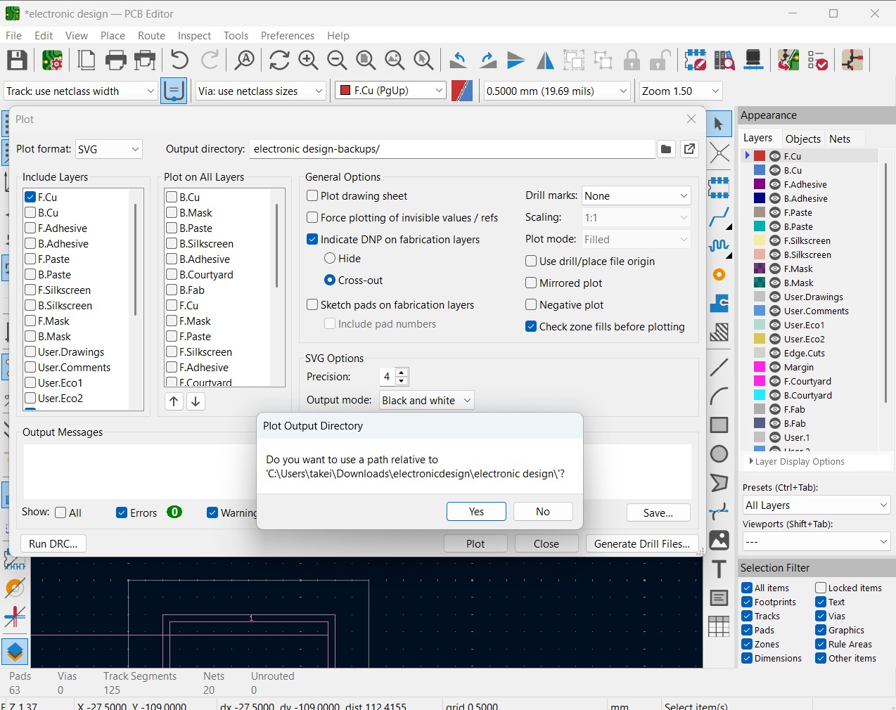
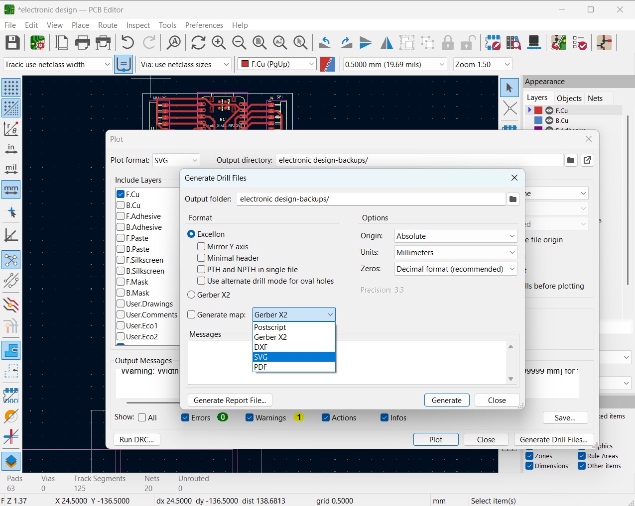
Making SVG Files for G-code
I saved the file in the directory where i would get it to covert to G-code by clicking file-plot
I selected the SVG file to make it ready to convert to gcode. The file is now ready for use.
File ready to be sent to mod
Making use of Mods
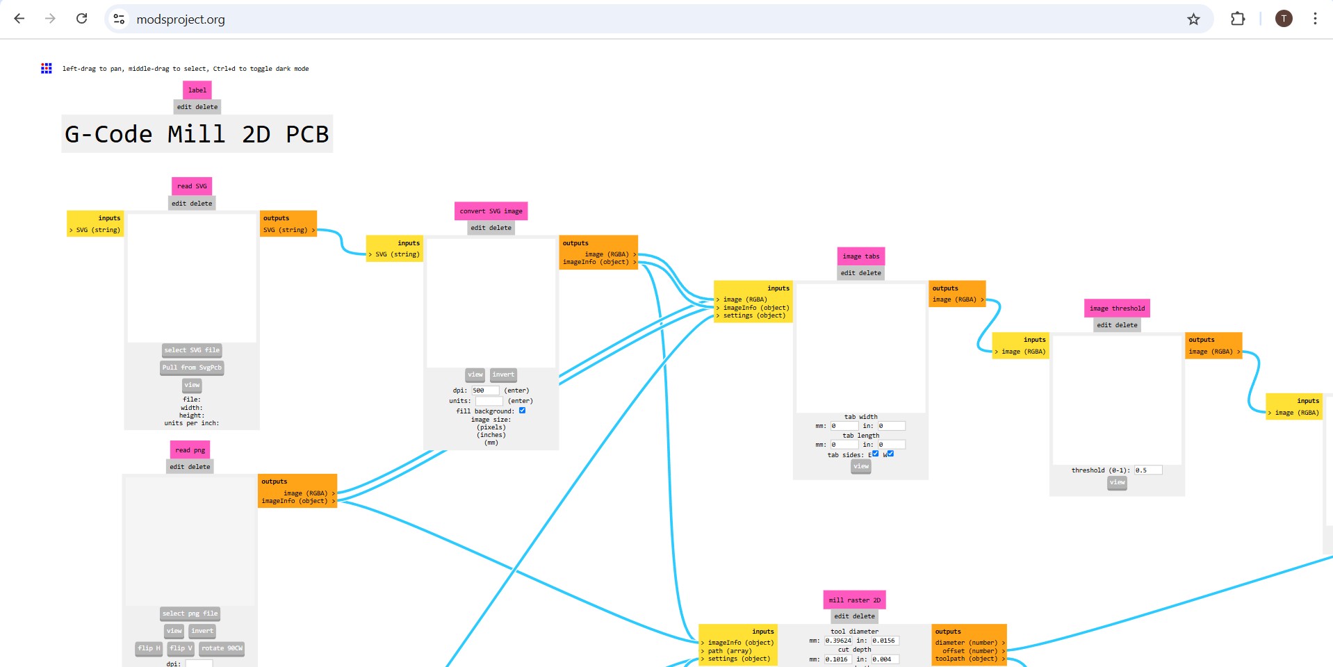
What is Mods CE in the Context of G-code Generation?
Mods CE (Community Edition) is a web-based, open-source platform developed by the MIT Center for Bits and Atoms
(CBA) for the Fab Lab community. It generates G-code for CNC machines, 3D printers, and other fabrication tools by
connecting modular workflows. Each module performs a specific task, such as reading files, processing images, generating
toolpaths, or outputting G-code. In this project, Mods CE is used to generate G-code for milling the PCB of the XIAO
RP2040 development board.
Mods CE Workflow:
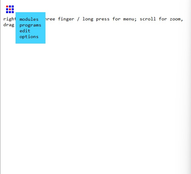
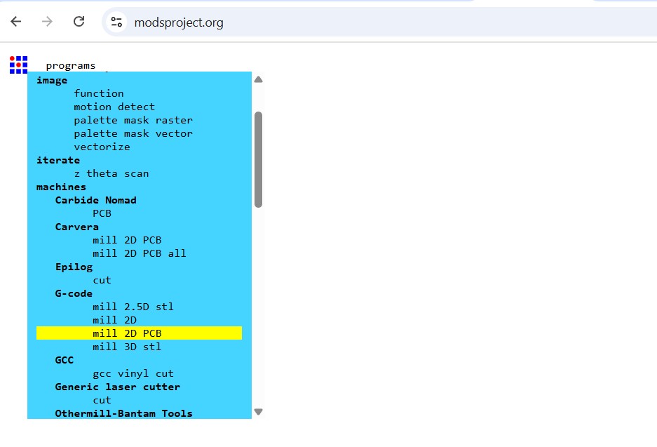
Open a browser and navigate to the Mods CE platform.
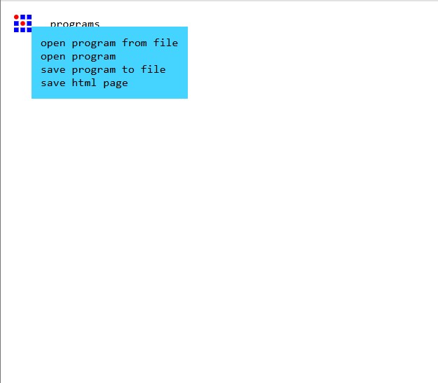
Right-click on the interface and select "Programs" > "Open Program" > "G-code" > "Mill 2D PCB."
A set of modules appears on the screen.
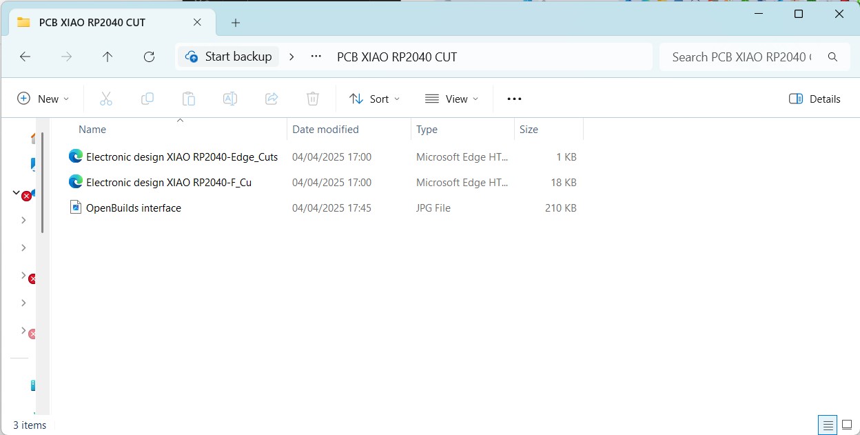
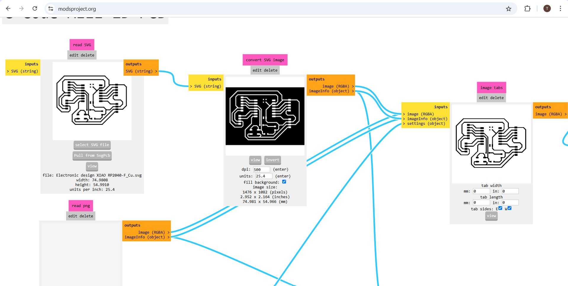
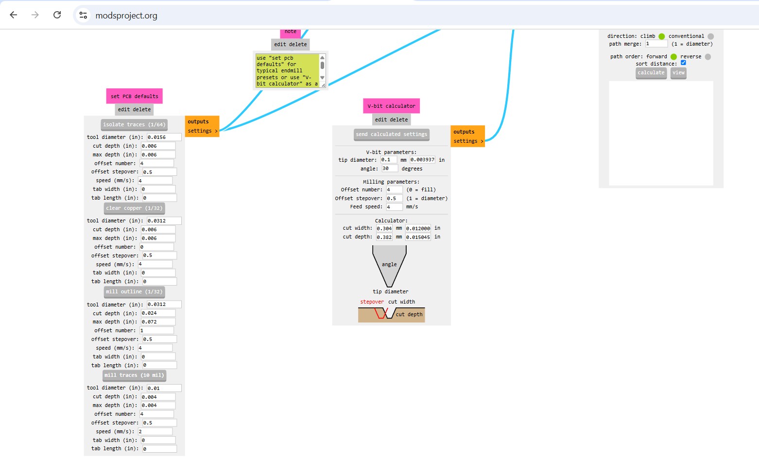
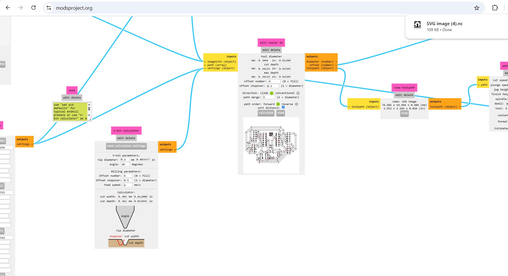
Save an SVG file and concvrt it to G-code
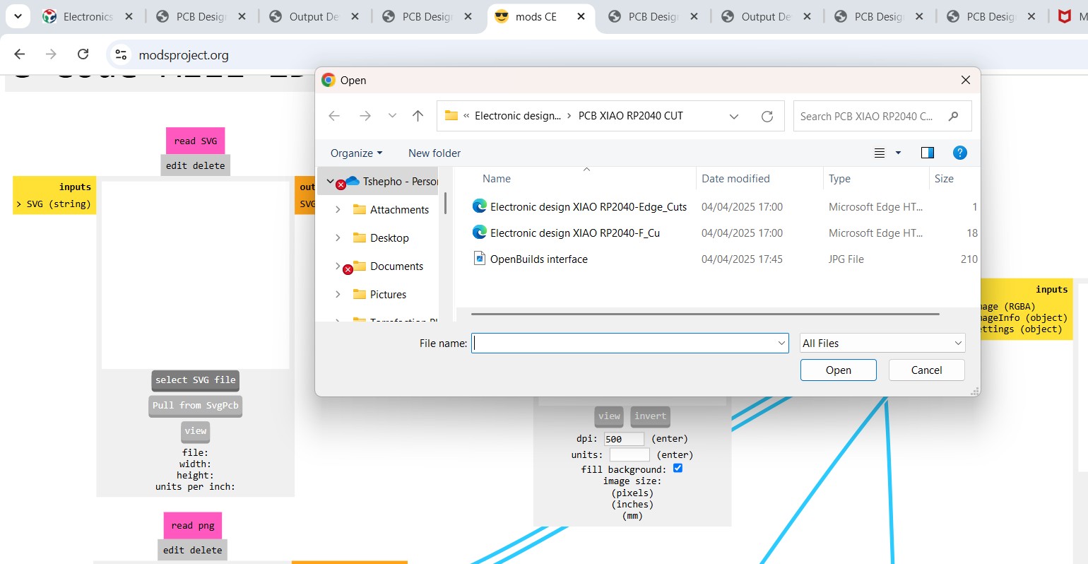
Uploading the svg file from where I saved it
SVG File Open in Mods workflow
Mill Traces and inputing v-bit parameters
Sending and calculated setting to Mill Raster 2D
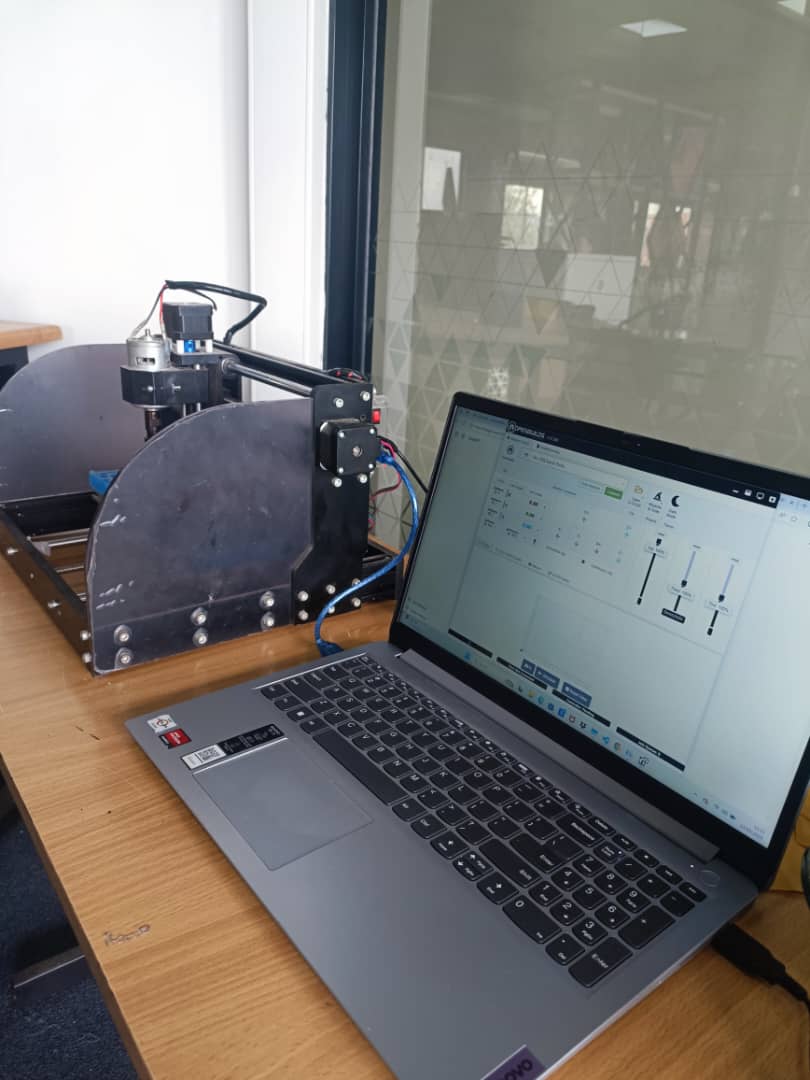
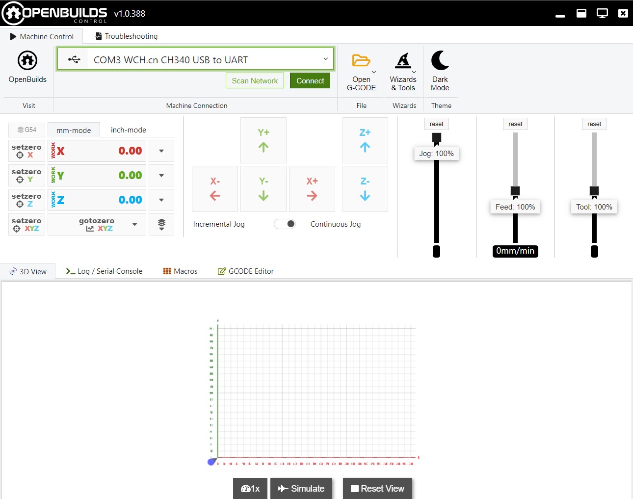
Transitioning to OpenBuilds Software for Control the CNC Mill with OpenBuilds CONTROL
OpenBuilds CONTROL replaces Universal G-code Sender (UGS) for sending the G-code to your CNC mill and controlling the machine.
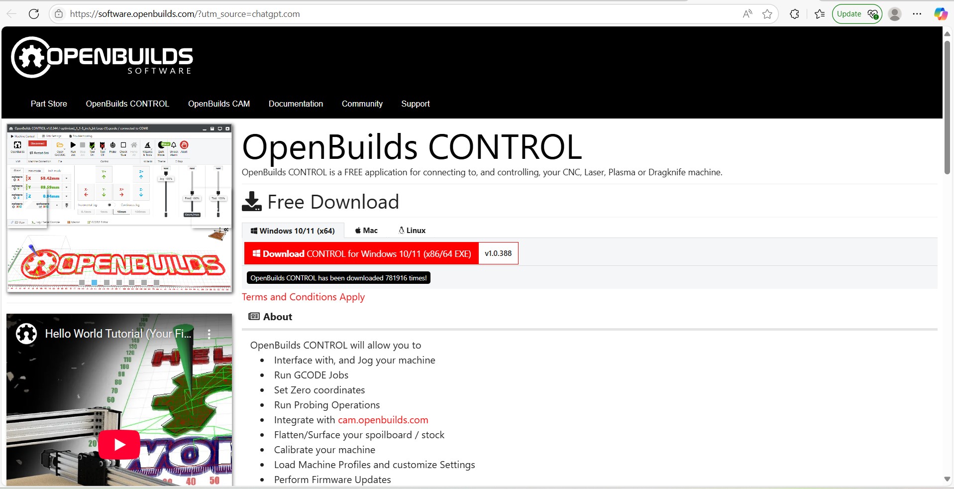
Install OpenBuilds Control
Download OpenBuilds CONTROL from software.openbuilds.com. It’s available for Windows, macOS, and Linux.
Connect to the CNC Mill:
Connect the CNC mill to my computer via USB. OpenBuilds CONTROL supports GRBL controllers,
whichthe PCB mill uses.
Open the application, select the correct port, and connect to the machine
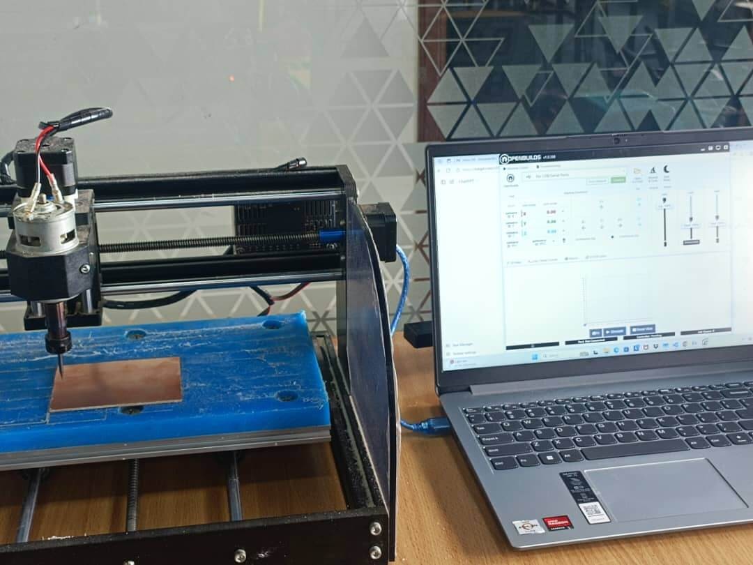
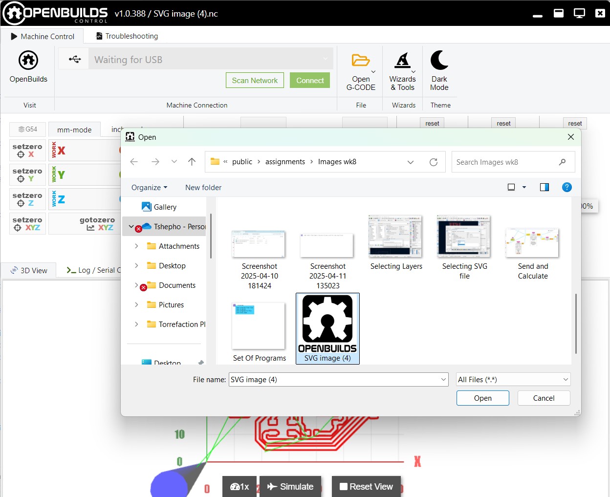
Load and Run the G-code:
Import the G-code file (board.nc) generated by OpenBuilds CAM.
Use OpenBuilds CONTROL to jog the machine, set the zero position, and verify the toolpath using its 2 & 3D G-code viewer.
Size the PCB board on KiCad
The layout is practical for a single-layer design, though a double-layer board could improve signal integrity with a ground plane.
5. Prototype Fabrication
Question:
Decide on a fabrication method (in-house production or professional board house).
Answer:
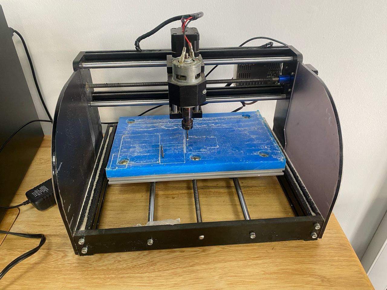
The board was fabricated using an in-house method using a PCB Milling machine
In-house PCB Milling Machine at UNIPOD Rwanda
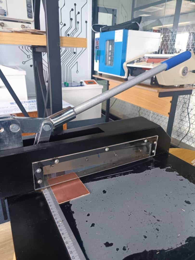
Cutting the Copper-clad board to the size of the PCB
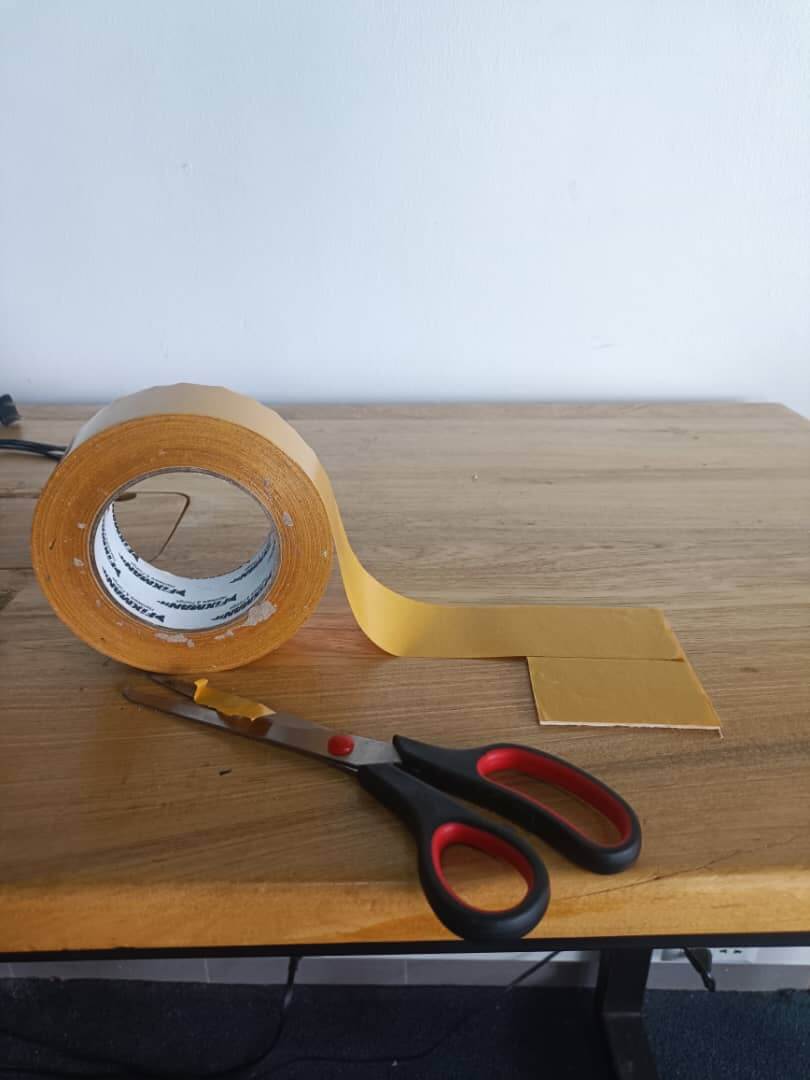
Use a double sided tape to stick the board to the base of the machine and place it
Set the Machine for cutting
Sizing Depth of Cut
Run the G-code to mill the PCB on the copper-clad board.
Video Milling PCB inhouse at UNIPOD Rwanda>
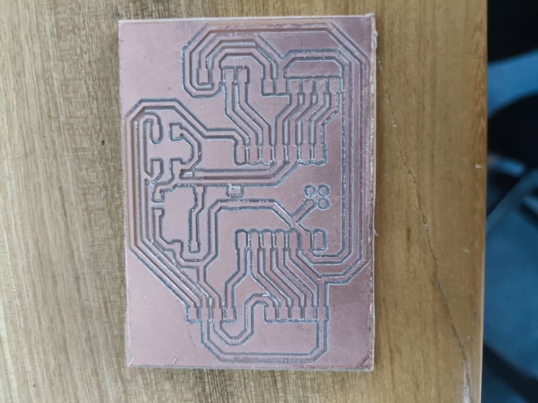
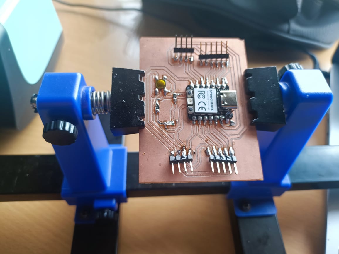
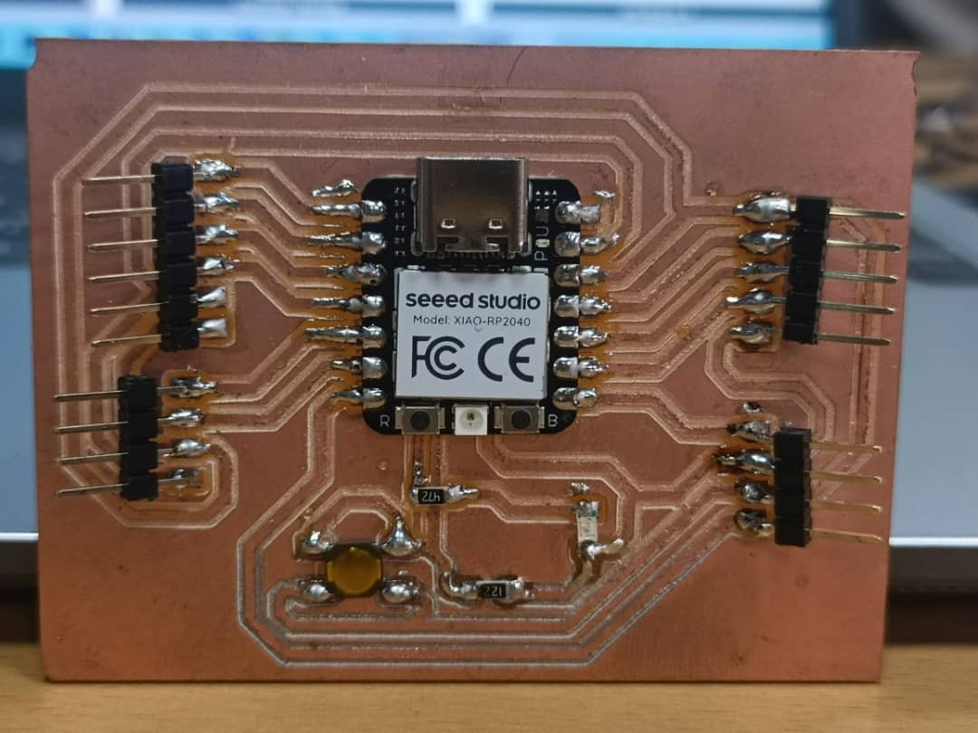
Completed PCB Traces
Fabrication Method: The board was created using PCB milling. The copper-clad board shows milling marks (white lines separating traces),
typical of a CNC milling process. The absence of solder mask and silkscreen (except for the XIAO RP2040’s markings) confirms in-house production.
In-House Setup: A Custom PCB milling machine was used. The single-layer design with wide traces (0.800 mm) matches the capabilities of desktop milling machines.
This method allows quick iteration for prototyping.
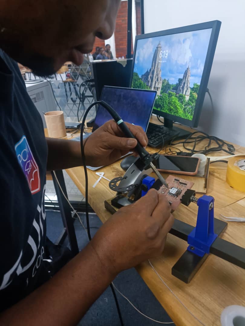
6. Assembly
Question:
Solder the components onto the fabricated PCB, use appropriate soldering techniques, and inspect solder joints.
Answer:
The assembly process includes:
Soldering: The XIAO RP2040, pin headers, USB-C connector, resistors, LED, and tactile switch are soldered onto the board. Solder joints are shiny and smooth, indicating proper soldering at around 300°C for lead-free solder.
Techniques: A fine-tip soldering iron was used to avoid thermal damage. For multi-pin components like headers and the USB-C connector, one pin was soldered first to secure the component, followed by the remaining pins.
Inspection: Solder joints are clean, with no bridges or cold joints. Components are aligned, and the XIAO RP2040’s castellated edges are well-soldered to the PCB pads.
The assembly is successful, with all components securely attached.
7. Testing and Validation
Question:
Develop a testing plan to verify each functionality, use debugging tools, and ensure all interfaces operate as intended.
Answer:
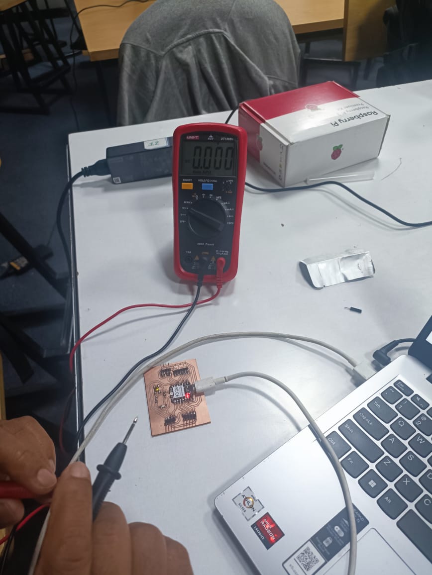
The testing plan to verify functionality includes:
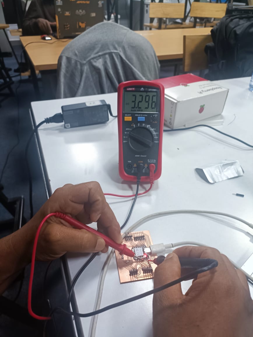
Power Supply Test: Connect the board to a USB-C 5V source. Use a multimeter to confirm the XIAO RP2040’s 3.3V output on a header is stable. Check for excessive heat indicating a short circuit.
Multimeter at Zero Volts
Multimeter at 3.3 Volts
Power Supply Test
The XIAO RP2040 has a built-in RGB LEDs, which are goodt for testing without external components. The onboard LED pins are:
Red: GPIO 17
Green: GPIO 16
Blue: GPIO 25
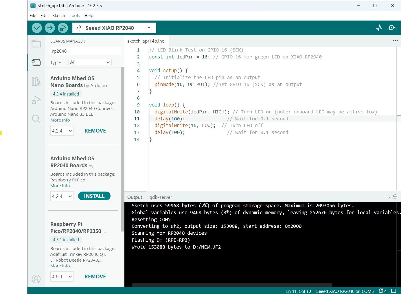
I used the green LED (GPIO 16 with the pin identified SCK on the PCB Design) to test the board.
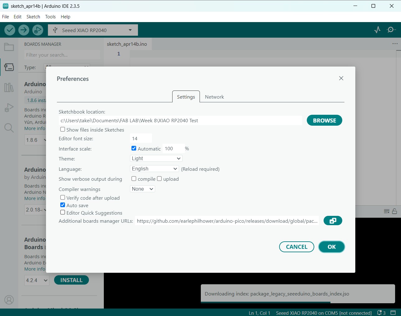
Install the Board
Install the package by Earle F. Philhower III and do the LED Blink Test
LED Test: Write a program Arduino IDE to toggle the LED on a GPIO pin. If the LED lights up, the GPIO output and LED circuit function.
Code Snippet LED GPIO 16:
// LED Blink Test on GPIO 16 (SCK)
                            const int ledPin = 16; // GPIO 16 for green LED on XIAO RP2040

                            void setup() {
                              // Initialize the LED pin as an output
                              pinMode(16, OUTPUT); //Set GPIO 16 (SCK) as an output
                            }

                            void loop() {
                              digitalWrite(ledPin, HIGH); // Turn LED on (note: onboard LED may be active-low)
                              delay(100);               // Wait for 0.1 second
                              digitalWrite(16, LOW);  // Turn LED off
                              delay(100); // Wait for 0.1 second
                            }
Video of the Green LED Blinking
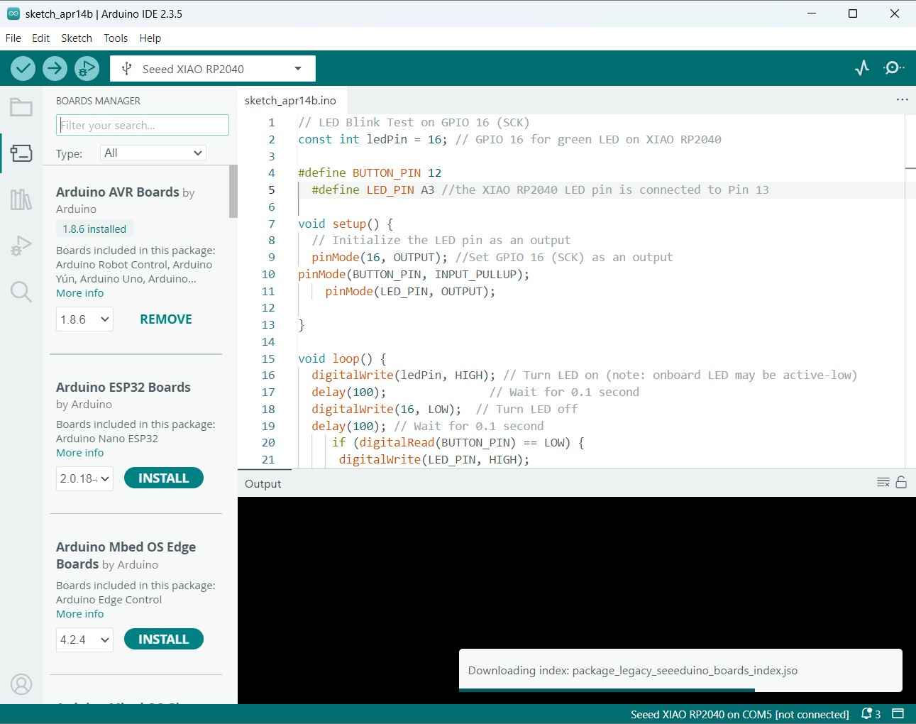
Switch Test: Program the RP2040 to detect the reset switch (SW1) state, printing a message to the serial monitor (via UART) when pressed, verifying the switch and reset functionality.
Switch (SW1) Test
Code Snippet LED GPIO 16 and SW1 Combined:
// LED Blink Test on GPIO 16 (SCK)
                                const int ledPin = 16; // GPIO 16 for green LED on XIAO RP2040

                                #define BUTTON_PIN 12
                                  #define LED_PIN A3 //the XIAO RP2040 LED pin is connected to Pin 13

                                void setup() {
                                  // Initialize the LED pin as an output
                                  pinMode(16, OUTPUT); //Set GPIO 16 (SCK) as an output
                                pinMode(BUTTON_PIN, INPUT_PULLUP);
                                    pinMode(LED_PIN, OUTPUT);

                                }

                                void loop() {
                                  digitalWrite(ledPin, HIGH); // Turn LED on (note: onboard LED may be active-low)
                                  delay(100);               // Wait for 0.1 second
                                  digitalWrite(16, LOW);  // Turn LED off
                                  delay(100); // Wait for 0.1 second
                                     if (digitalRead(BUTTON_PIN) == LOW) {
                                      digitalWrite(LED_PIN, HIGH);
                                    } else {
                                      digitalWrite(LED_PIN, LOW);
                                    }