Electronics Design
Group Assignment: Microcontroller Circuit Board Observation
Link to Group Assignment Page
Shared group findings on a centralized page: Visit our Group Assignment Page
Individual Assignment: Design and Check a Development Board
Design Documentation
Lessons Learned:
Adding Symbol Libraries:I learned to manage and import symbol libraries in KiCAD, ensuring the Xiao-RP2040 (M1)
and other components (LED D1, tactile switch SW1, resistors R1 and R2) had accurate symbols by cross-referencing
datasheets. I mastered searching for symbols (e.g., SWITCH_TACTILE_OMRON for SW1) and importing community libraries
for the Xiao-RP2040.
Adding Footprint Libraries: I gained expertise in associating symbols with footprints, selecting appropriate footprints
for the Xiao-RP2040 (surface-mount module), headers (2.54mm pin headers), and through-hole components (e.g., LED, resistors).
I learned to verify footprint dimensions for soldering and preview them in the Footprint Editor.
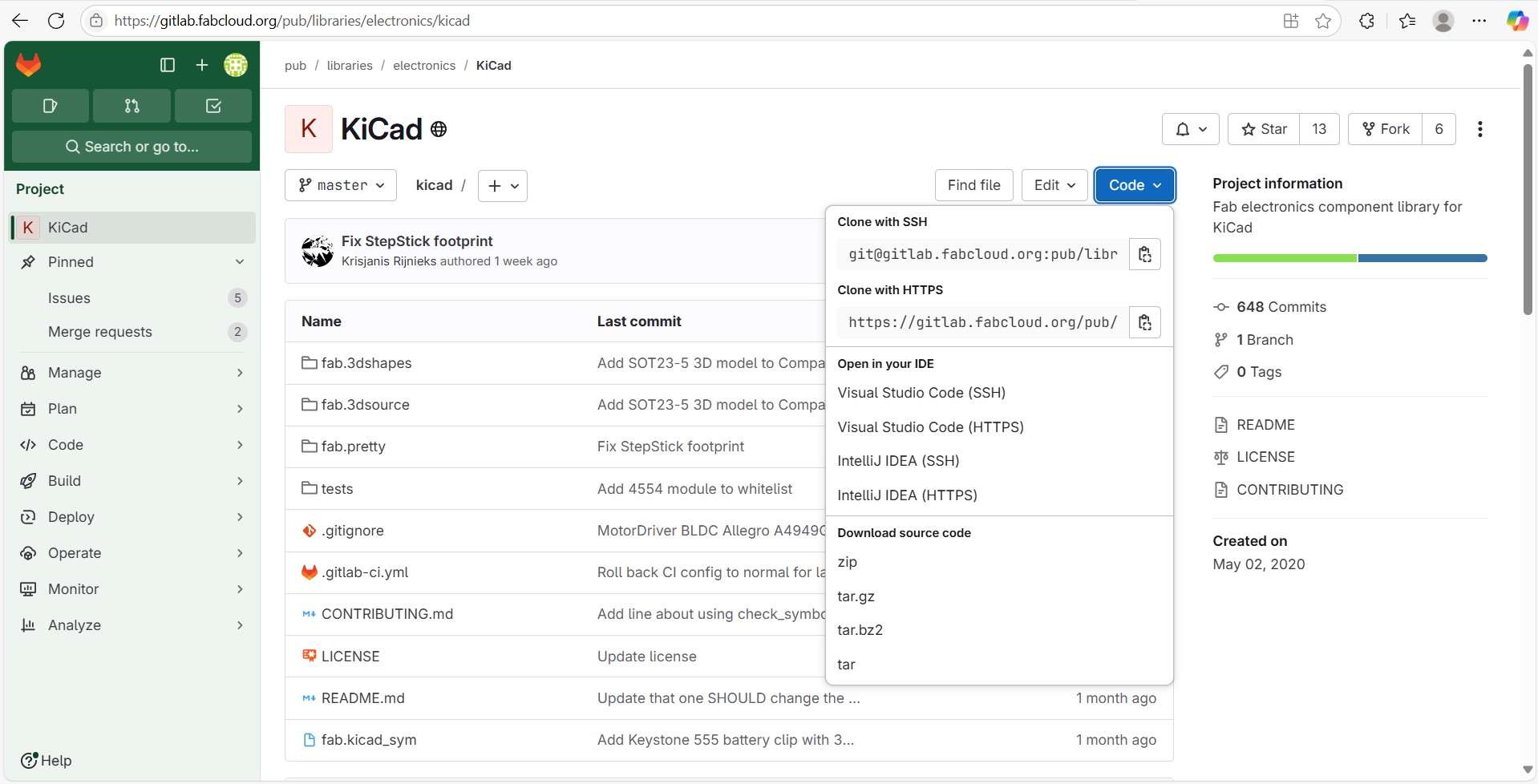
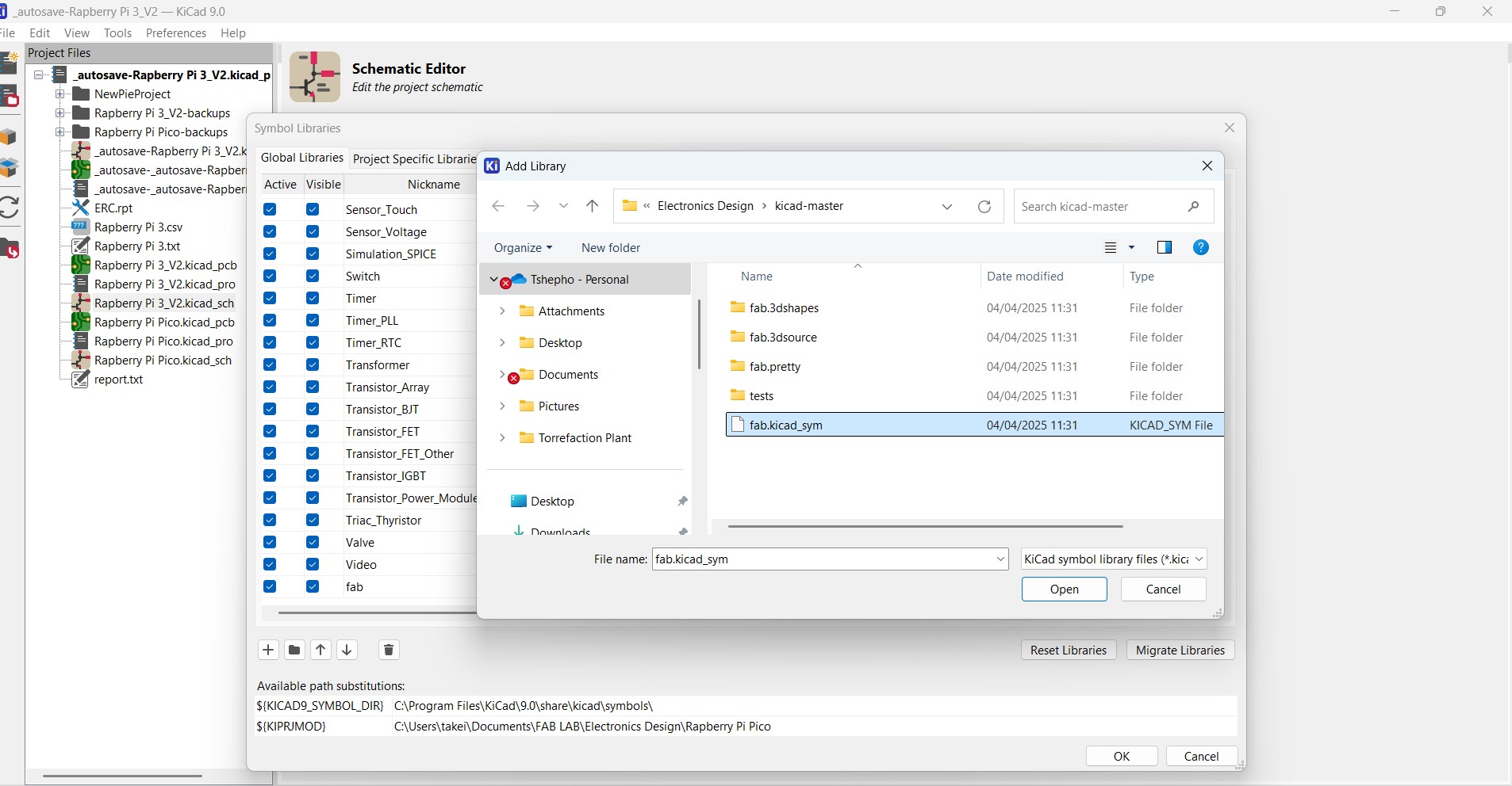
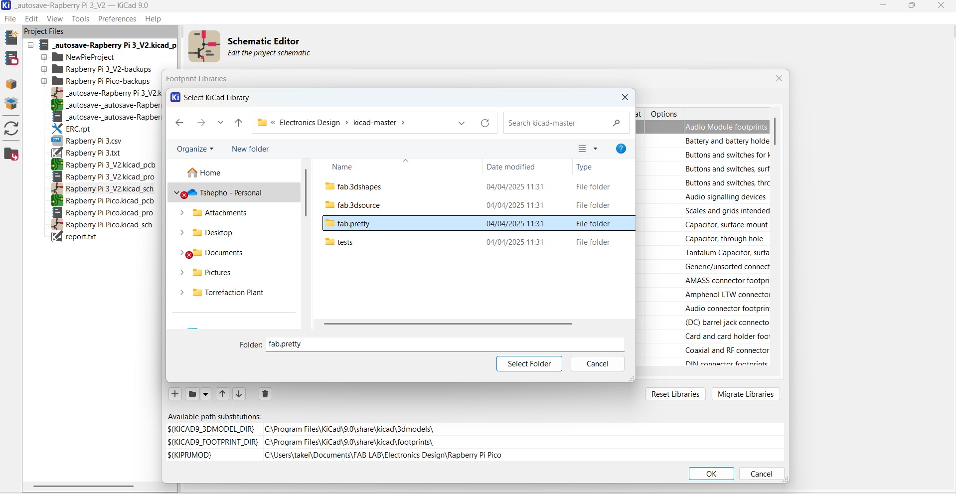
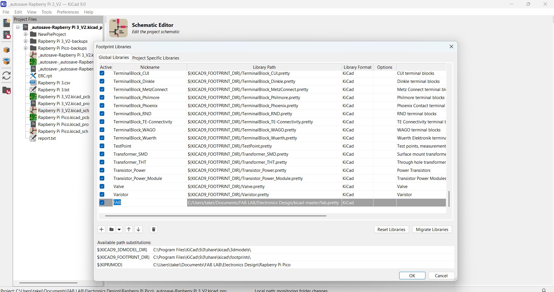
Link to Fab libraries
Placing Symbols:I learned to arrange symbols logically in the schematic, placing the Xiao-RP2040 centrally and grouping
related components (e.g., LED D1 and resistor R1 near pin D0, switch SW1 and resistor R2 near pin D1). I positioned connectors
(J2-J5) to reflect their intended PCB layout, improving the design workflow.
Placing Footprints:I prepared for PCB layout by assigning correct footprints in the schematic and later placing them in
the PCB editor, ensuring ergonomic placement (e.g., headers on edges for accessibility) and correct orientation (e.g., LED cathode
aligned with GND).
Placing Global Labels:I learned to use global labels to manage power nets like VCC and GND, as well as placing net sconnecting
the Xiao-RP2040’s VIN and GND pins, headers (J2-J5), and other components (e.g., R1, R2) without drawing wires. I understood the
difference between global and regular labels, standardized naming (e.g., VCC for 3.3V), and placed labels strategically for clarity.
For example, nets such as VCC, GND, SCL, SDA, and TX/RX can be labeled globally so that they are connected to the appropriate pins on
1modules like the RP2040 or external connectors like I2C or UART headers. This was particularly useful in keeping my schematic clean
and readable, especially when routing signals to multiple headers like J2
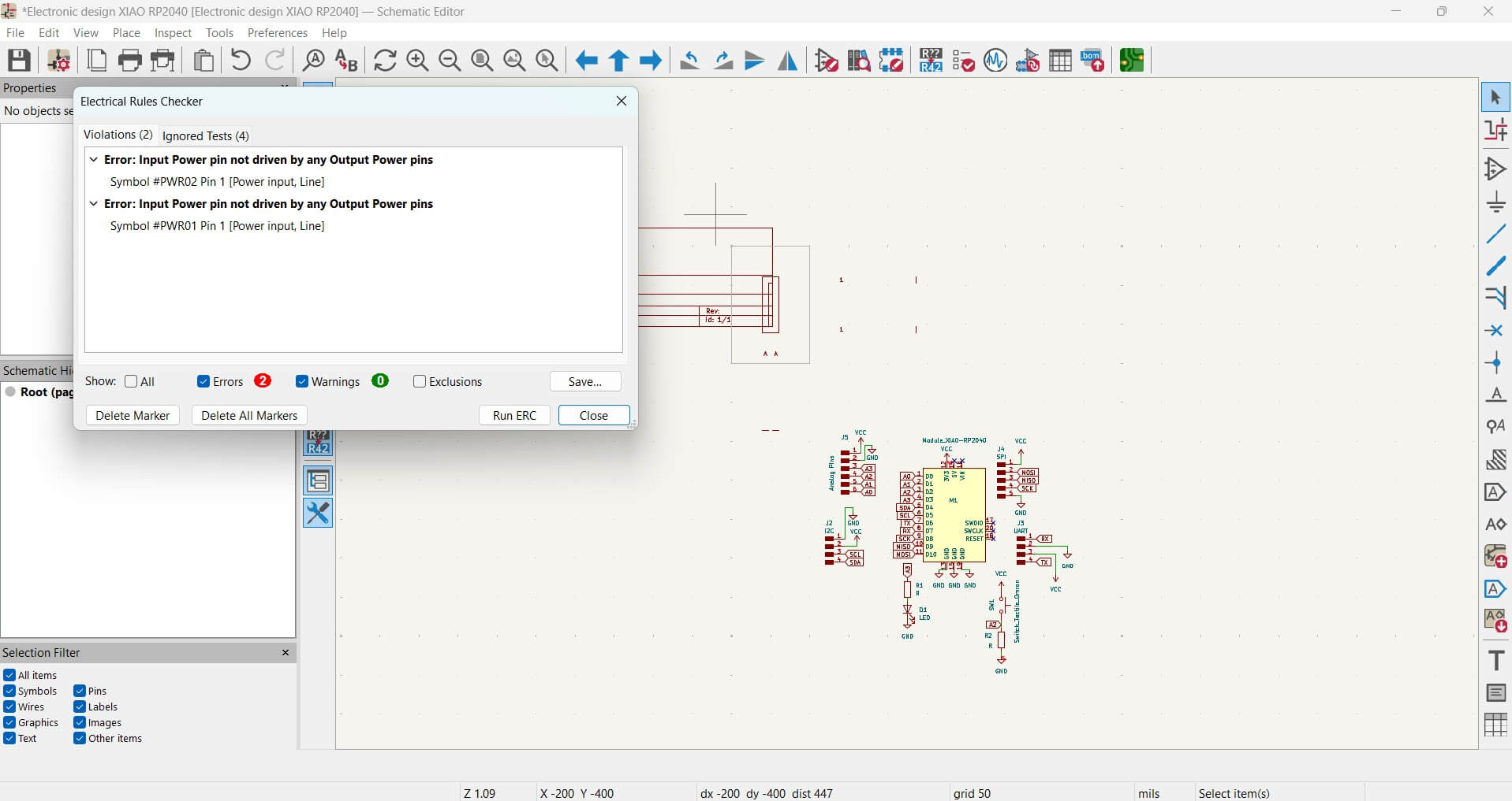
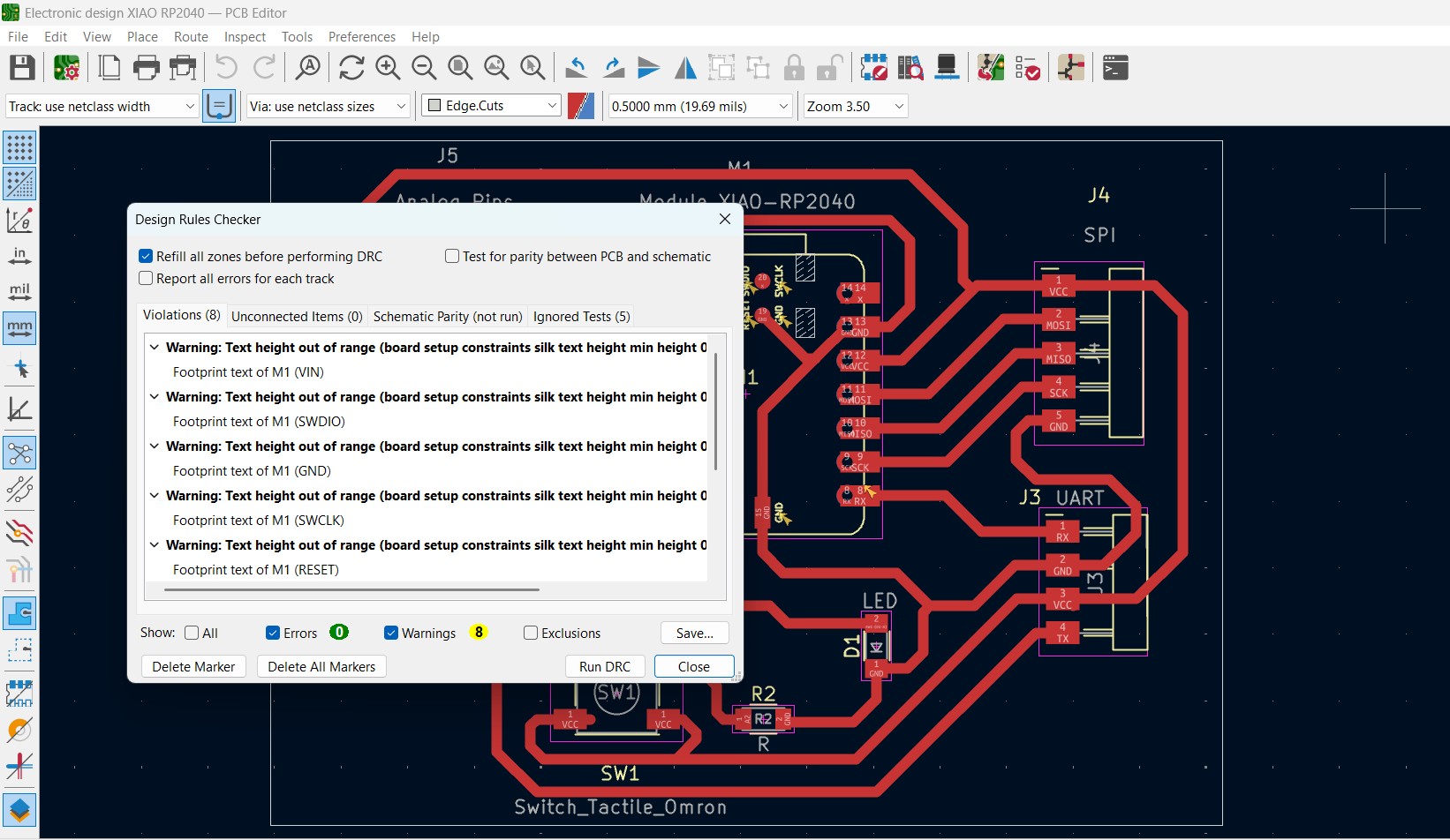
Design Rules Check (DRC):I used the Electrical Rules Check (ERC) to catch errors like unconnected pins (e.g., unused Xiao-RP2040
pins) and missing power connections (e.g., LED circuit initially missing VCC). I learned to interpret ERC warnings, fix critical issues,
and run checks frequently to catch errors early.
Problems and Solutions:
Initially, Used Raspberyy Pi Pico as a microcontroler for my stepper motor becasue I did not have the Pi Pico at my
University in Botswana. By then I was not aware of the global lables when i drew the Circuit. To check whether the
circuit works I used Electrical Rules Check (ERC) and it overwhelmed me with a barrage of warnings and errors. This made
me to learn how to interpret these messages. I discovered that some warnings—such as unused pins—were acceptable
based on my design intent, while others—like missing connections—were critical and needed immediate attention. Below is
an image of the Pi Pico design that I made then.
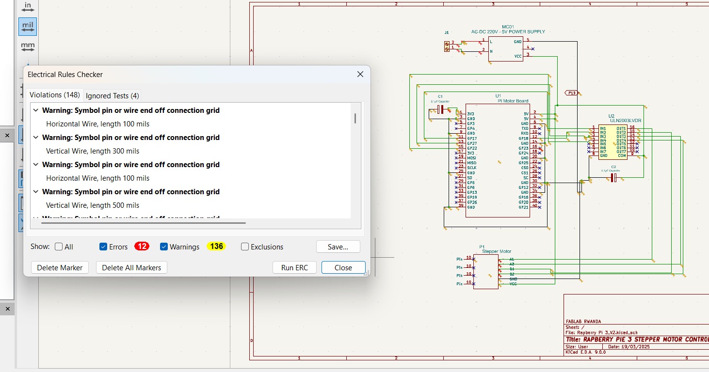
One key insight was the importance of running the ERC frequently throughout the design process rather than waiting until the end. This helped me catch
issues early and prevented them from being carried over into the PCB layout phase, saving a lot of time and effort later on.
When I arived in Kigali at the UNIPOD I learnt the use of global labels and I changed from using the Pi B to XIAO RP2040. When I finished drawing the
circuit and this reduced the number of visual connections on the schematic, making it cleaneras compare , but they also significantly improved the PCB
layout experience. With clearly defined connections to every component from the RP2040, I was able to route the PCB more efficiently and with greater confidence in the correctness of the connections.
Design Files
Schematic, PCB layout and BOM files created in KiCAD:
Schematic-KiCad
PCB layout
Bill of Materials
| Item No | Value | Qty | Reference | Footprint | Datasheet | Description |
|---|---|---|---|---|---|---|
| 1 | Switch, Tactile, Omron | 1 | SW1 | FAB-Button_Omron_B3SN_6.0x6.0mm | Link | Push button switch, Omron, B3SN, Sealed Tactile Switch (SMT), SPST-NO Top Actuated Surface Mount |
| 2 | R | 2 | R1, R2 | FAB-R_1206 | - | Resistor |
| 3 | Module_XIAO-RP2040 | 1 | M1 | FAB-SeeedStudio_XIAO_RP2040 | Link | XIAO RP2040 - ARM® Dual-Core Cortex®-M0+ MCU 32-Bit Embedded Evaluation Board |
| 4 | Analog Pins | 1 | J5 | FAB-PinHeader_0.1x06_P2.54mm_Horizontal_SMD | Link | Connector Header Through Hole 6 positions 0.100" (2.54mm) |
| 5 | SPI | 1 | J4 | FAB-PinHeader_0.1x05_P2.54mm_Horizontal_SMD | - | Male connector, single row |
| 6 | UART | 1 | J3 | FAB-PinHeader_0.1x04_P2.54mm_Horizontal_SMD | - | Male connector, single row |
| 7 | I2C | 1 | J2 | FAB-PinHeader_0.1x04_P2.54mm_Horizontal_SMD | - | Male connector, single row |
| 8 | LED | 1 | D1 | FAB-LED_1206 | - | Light emitting diode |
Fabrication Check
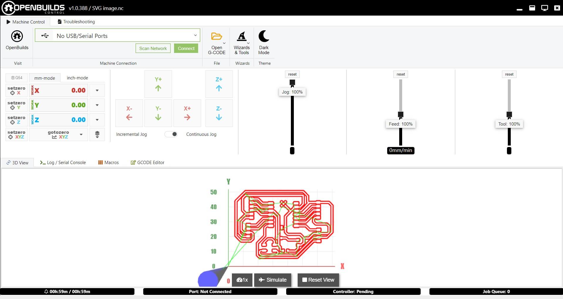
Ran a Design Rule Check (DRC) in KiCAD. Adjusted trace spacing to meet fabrication requirements. Exported and verified SVG file.
SVG File Preview:
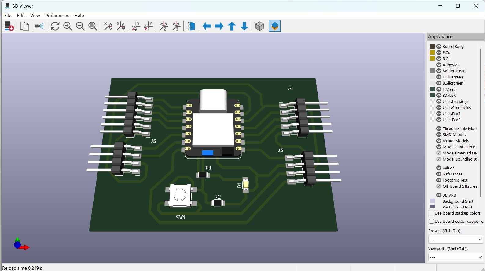
Hero Shot
3D rendering of the development board:
Zip Files for Downloads
Week 6 Design files for Download