Electronics Production
- Characterize the design rules for your in-house PCB production process: document feeds, speeds, plunge rate, depth of cut (traces and outline), and tooling.
- Document the workflow for sending a PCB to a boardhouse
- Document your work to the group work page and reflect on your individual page what you learned
- Make and test a microcontroller development board that you designed
#.Group assignment:

As a group, we established basic design rules for our in-house PCB production, including appropriate settings for milling traces and outlines. We also documented the workflow for sending a PCB to a boardhouse, which involved exporting design files, verifying them, and submitting them for fabrication.
Group assignment link
#.Individual assignment
Making and Testing a Microcontroller Development Board
1. The goal
The goal of this project was to design, fabricate, and test a microcontroller development board from scratch.
For this project, I chose to work with the XIAO-RP2040 Module, a compact yet powerful microcontroller. Before starting the design, I needed to ensure I had the correct components and libraries in my KiCad software.
The journey from an idea to a working circuit board involved several steps, including schematic design, PCB layout, generating G-code for milling, and testing the final board. Each phase presented its own challenges and learning experiences.
2. The Journey: Challenges and Decisions
setting up the design environment
The first step was setting up the design environment. I downloaded the KiCad library from FabCloud (link) and followed the installation steps to integrate it into my software. This was important because it provided a standardized library of electronic components, ensuring accuracy in my design. Without this, I could have faced compatibility issues when transferring the schematic to the PCB layout.
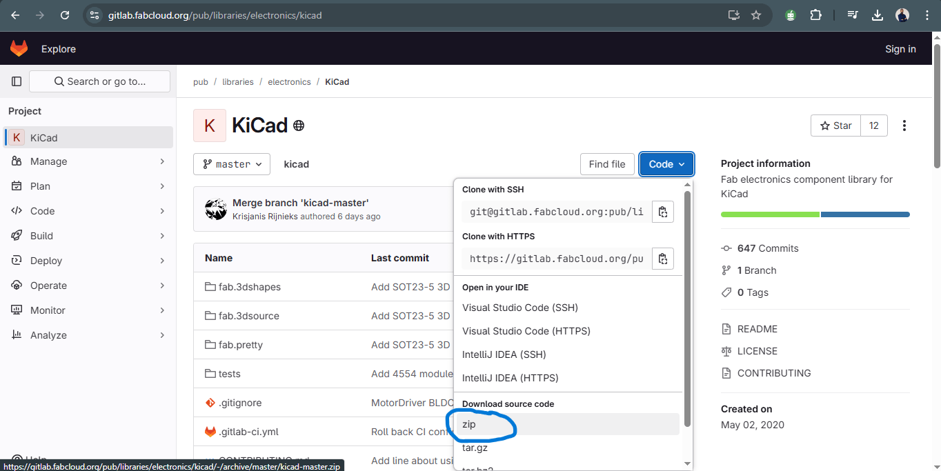
This is how i downloaded the KICadmaster from FabCloud
Next, I needed to understand the microcontroller I was using. I referred to the XIAO-RP2040 pinout and specifications from Seeed Studio. This was a crucial step, as misinterpreting the pin configuration could lead to major functionality issues. By carefully analyzing the datasheet, I ensured that the power, input/output, and communication pins were correctly assigned in the design.
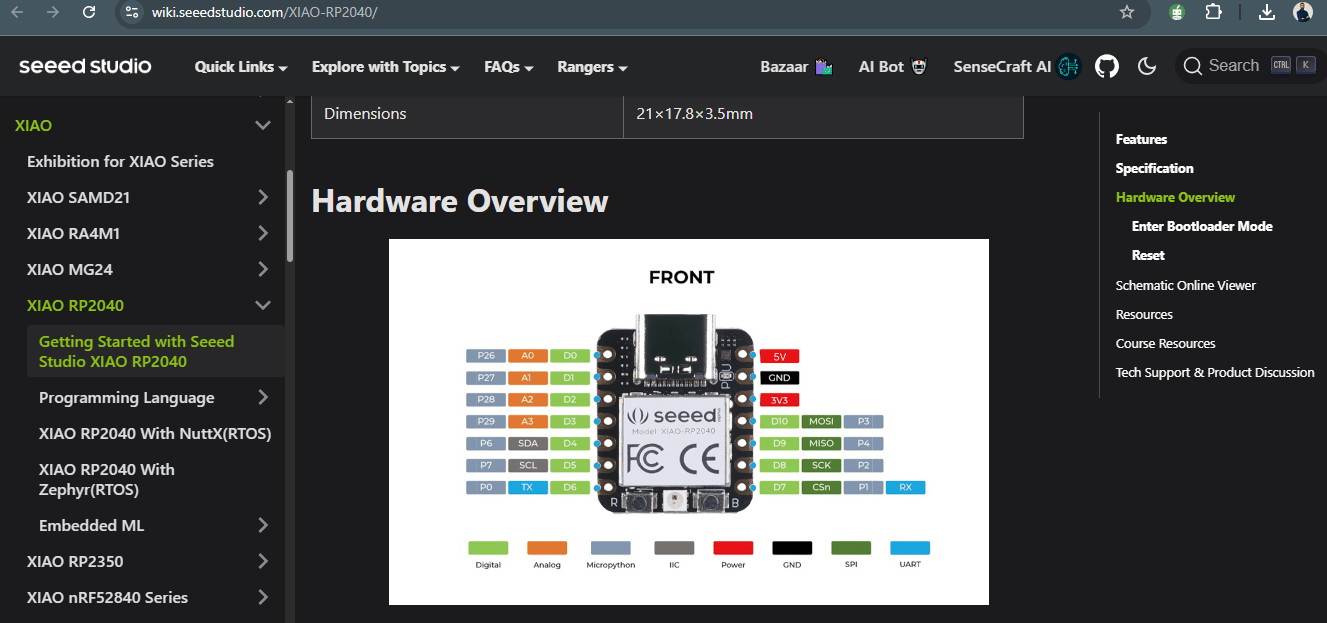
the XIAO-RP2040 pinout
The design
With the preparation done, I moved on to schematic design in KiCad. I created the circuit, making sure that each component was correctly placed and connected.
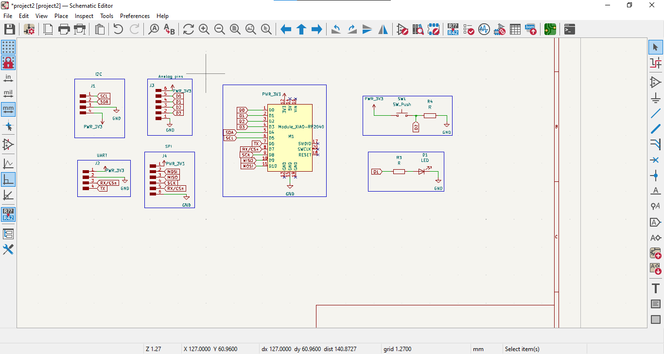
schematic design in KiCad
After verifying the connections, I transferred the schematic to the PCB editor, where I arranged the components and routed the traces. This stage required careful planning to minimize interference and ensure efficient signal flow.
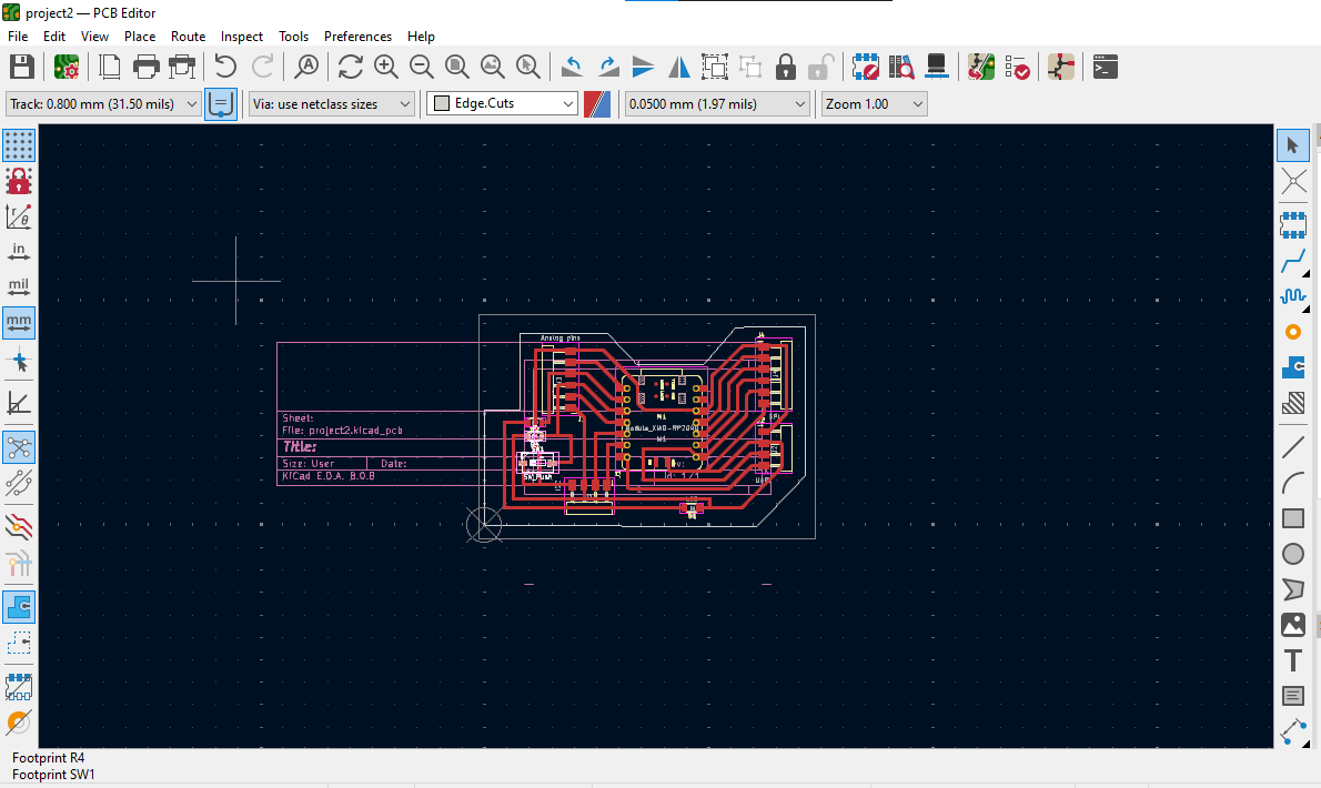
PCB editor
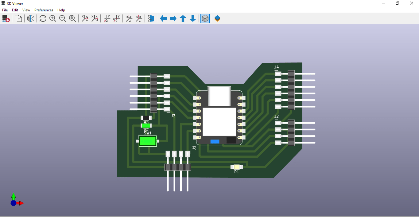
3D view
Once satisfied, I exported the design as an SVG plot, which would later be used for milling.
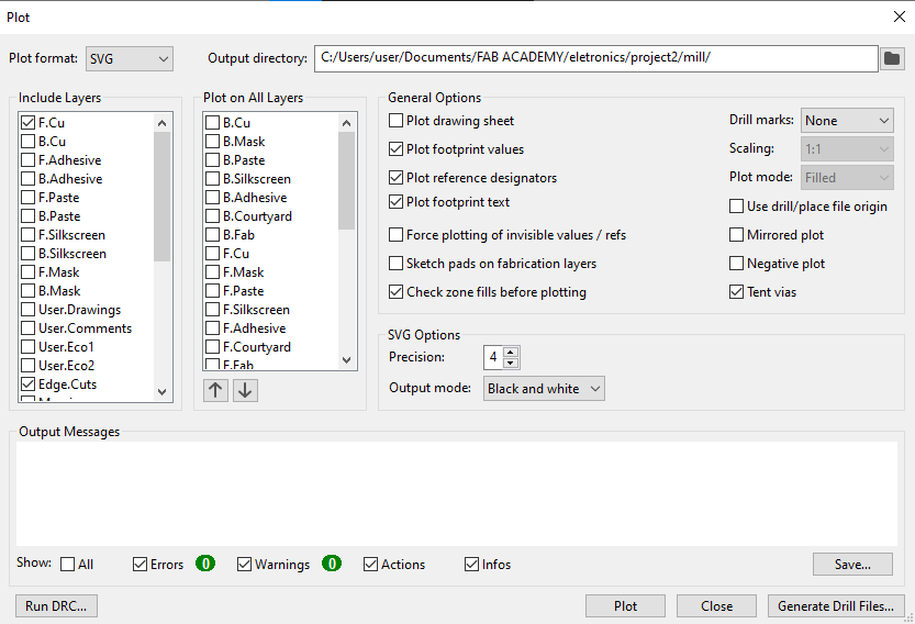
Saved SVG file
Generating G-Code
Now came the PCB production phase, where I had to convert my design into physical form. To generate machine instructions, I used ModsProject (link) to create the G-code required for PCB milling. This step was critical because any errors in the G-code could result in a failed or inaccurate PCB.
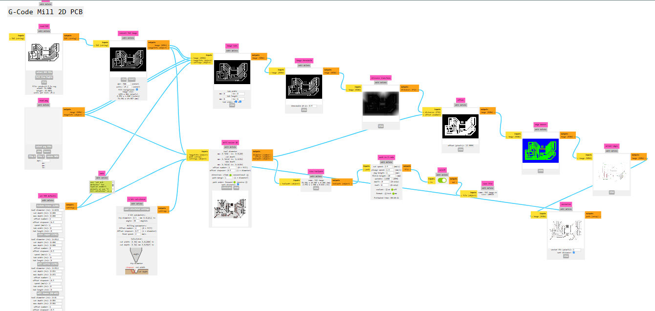
G-Code Mill 2D PCB
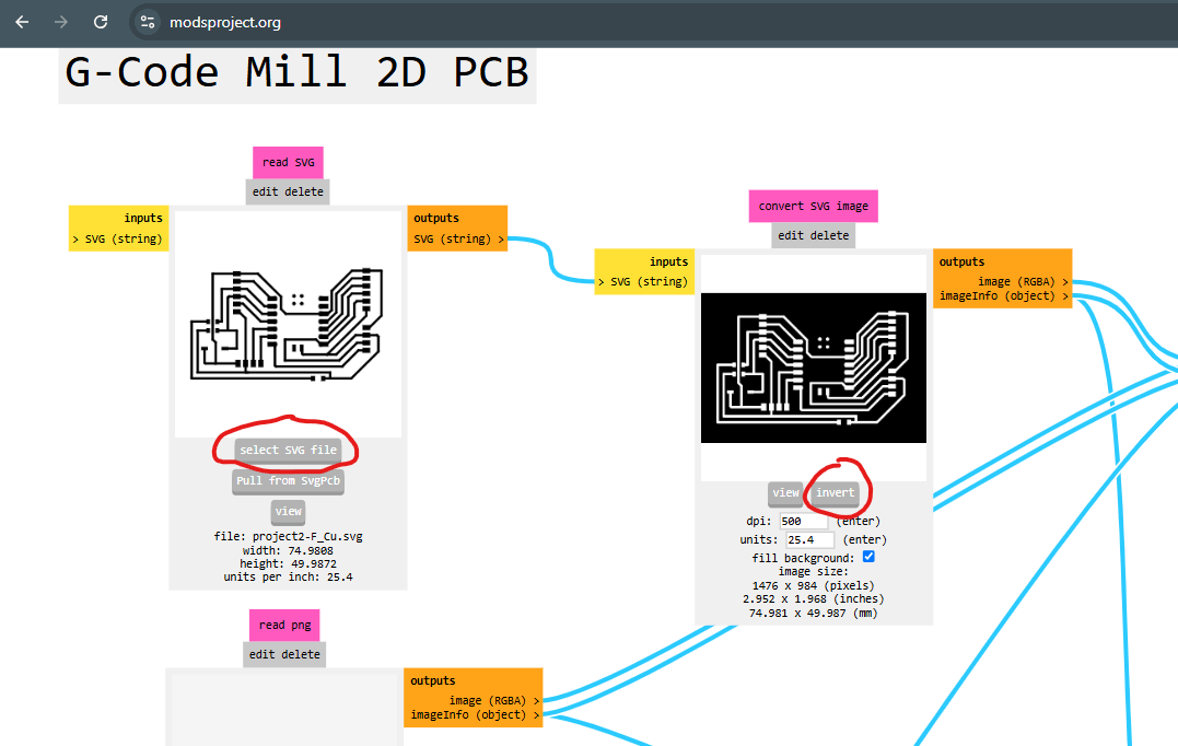
I started by selecting the SVG file i saved as showen, then i inverded it so that the routed traces will remain on my PCB.
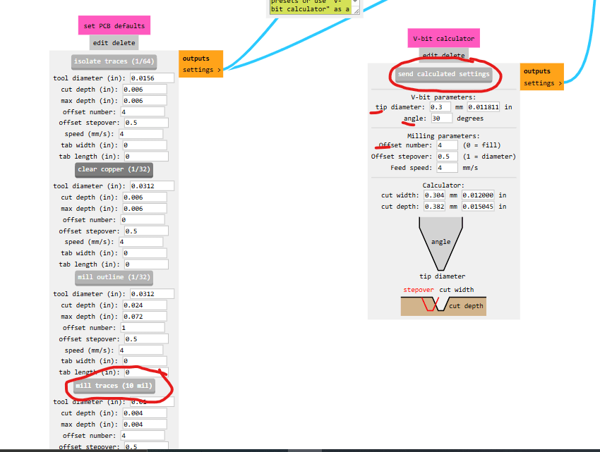
Then i moved down to the PCB defaults and select mill traces so that i can start by milling the traces of my PCB. then in v-calculator i checked the parameters and change some of them depending on the tool i was going to use;like the tip diameter to 0.3 and the offset nymber to 4. after all that i click on send calculated settings.
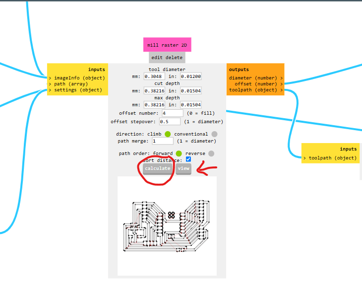
In the Mill raster 2D i viewed the job after i was satisfied i clicked on calculate and the job was downloaded.
Milling the PCB
After generating the G-code, I downloaded OpenBuilds software (link), which allowed me to load the design into the milling machine.
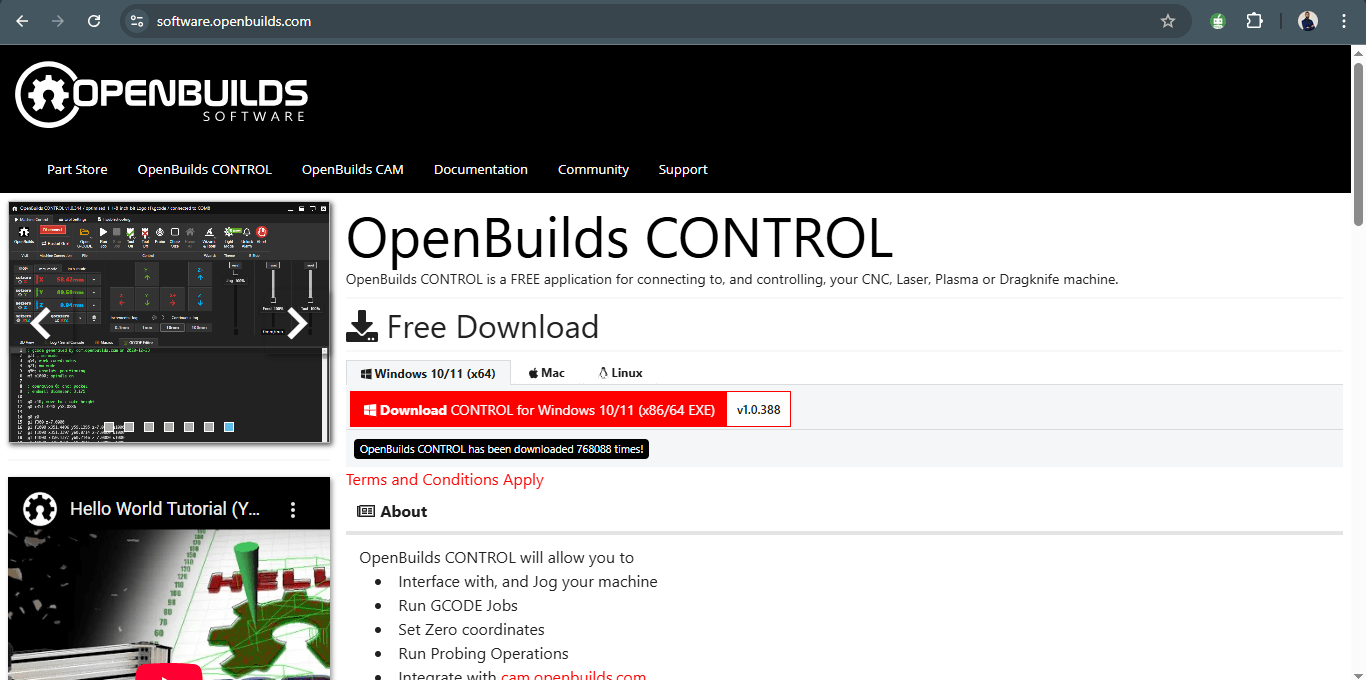
I downloaded OpenBuilds software
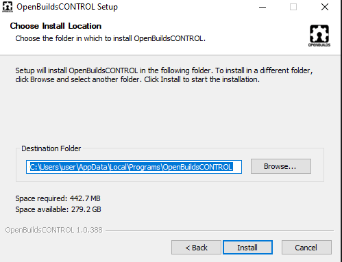
Then install it
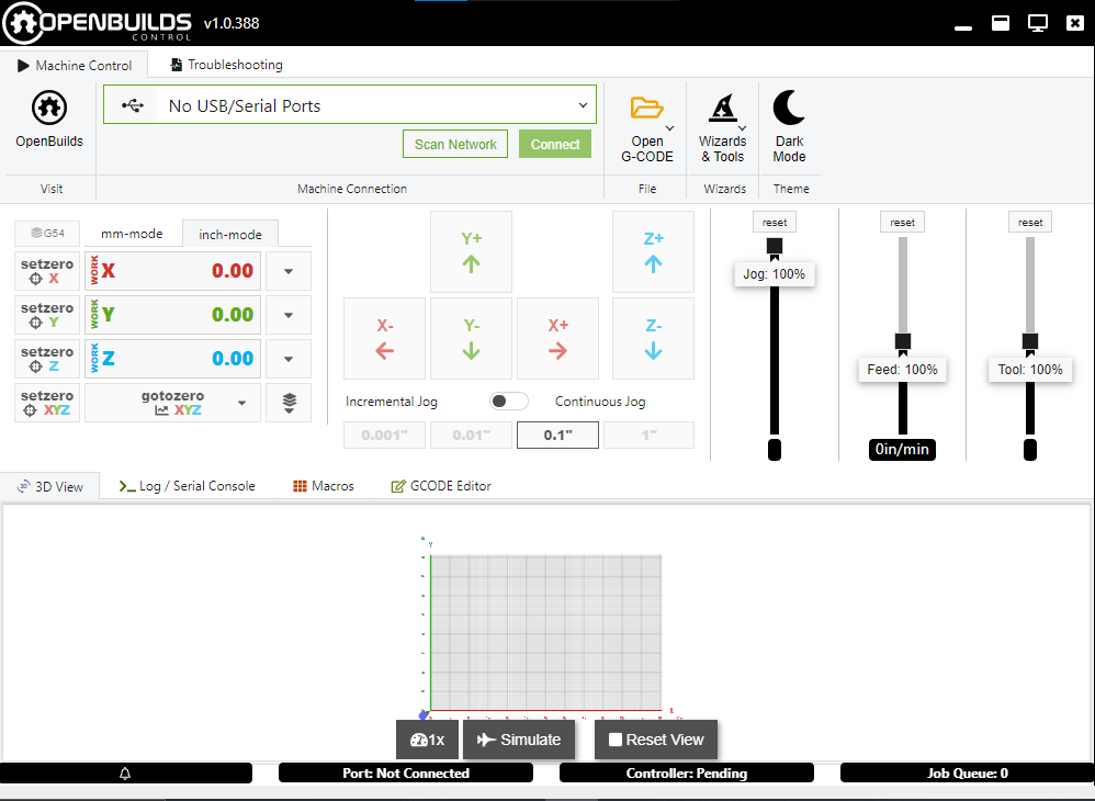
OpenBuilds software
With everything set, I carefully started milling the PCB. This process required precise calibration to ensure that the traces were correctly cut and that the copper was not over-etched. Small mistakes, such as improper depth settings, could lead to broken traces or poor conductivity. After milling, I inspected the board, ensuring that all traces and pads were intact before moving forward with soldering and testing.
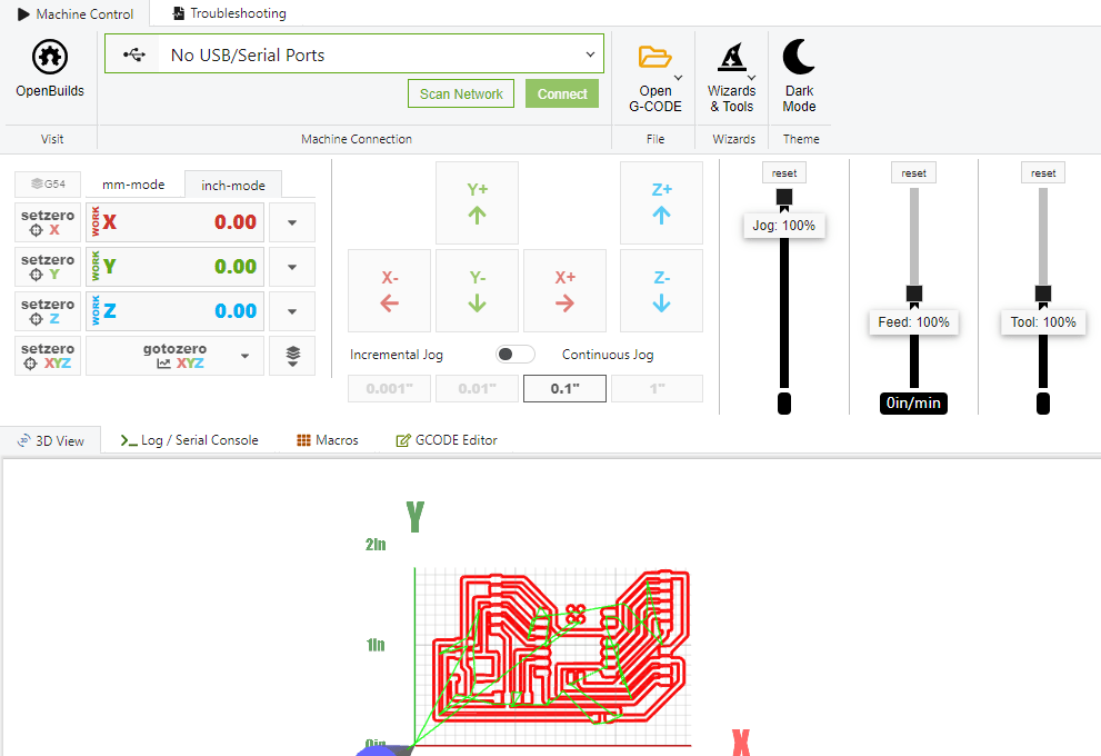
Openning my work in OpenBuilds software
Milling the PCB traces
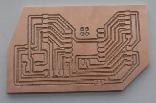
3. Testing the PCB
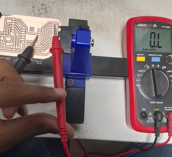
Electrical connections test
Once the PCB was milled, the next step was to test its electrical connections before soldering any components. The first thing I did was use a multimeter to check for continuity in the traces. This ensured that there were no broken connections or short circuits between adjacent traces. Any issues at this stage could mean going back and remilling the board, so careful inspection was necessary.
soldering
After confirming the traces were correct, I soldered the components onto the board. This required patience and precision, especially when working with surface-mounted components (SMDs), which can be difficult to place correctly. One mistake in soldering could cause connectivity issues, so I made sure to inspect every joint carefully.
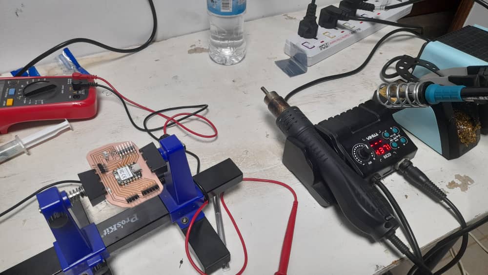
Microcontroller board test
Once soldering was completed, I powered up the board for the first time. The final step was to see If the LED blinked as expected, it confirmed that the board was properly designed and assembled. If not, I would have to troubleshoot by checking the solder joints, microcontroller connections, or potential firmware issues.
the LED blinked as expected, it confirmed that the board was properly designed and assembled.
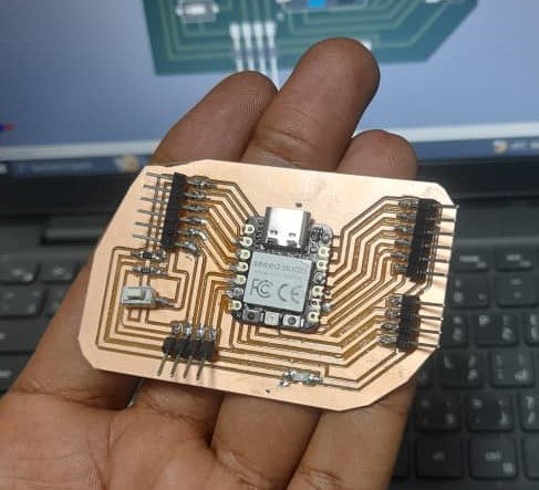
The final microcontroller development board
4. Reflection and Takeaways
Advice:
- Always double-check component footprints before designing the PCB to avoid mismatches.
- Use a multimeter after milling to test connections before soldering.
- Proper tool calibration is crucial for achieving clean PCB traces.
- This project reinforced my understanding of electronics production workflows, from design to manufacturing.
- It built confidence in using milling machines for rapid PCB prototyping.
- The knowledge gained will be invaluable for future IoT and embedded systems projects.
Design files
- download file (SVG mill file)
- download file (SVG file)