For this week, we had to complete both a group assignment and an individual assignment. In the group assignment, we used the test equipment in our lab to observe the operation of a microcontroller circuit board. As a minimum, we demonstrated the use of a multimeter and an oscilloscope. We documented our work on the group work page and reflected on what we learned on our individual pages.
In the individual assignment, we used an EDA tool to design a development board that uses parts from the inventory to interact and communicate with an embedded microcontroller. The learning outcomes for this assignment included selecting and using software for circuit board design and demonstrating the workflows used in circuit board design.
Group Assignment
For the group assignment, we used the test equipment in our lab to observe the operation of a microcontroller circuit board. As a minimum, we demonstrated the use of a multimeter and an oscilloscope. The full documentation of our group work can be found on our group assignment page.
Individual Assignment
For the individual assignment, I used KiCad, an open-source EDA tool, to design a development board that attaches to the ESP32 DevKit V1. KiCad offers a comprehensive suite of features for PCB design, including schematic capture, PCB layout, 3D visualization, and Gerber file generation. I started by creating the schematic, where I placed and connected various components such as resistors, capacitors, and connectors. KiCad's extensive library of components and its ability to create custom components made this process straightforward. After completing the schematic, I switched to the PCB layout editor to arrange the components on the board and route the traces. KiCad's design rule checks (DRC) ensured that my layout met the necessary electrical and manufacturing constraints. Once the layout was finalized, I used the 3D viewer to inspect the board and verify the placement of components. Finally, I generated the Gerber files required for manufacturing. To produce the PCB, I opted for isolation milling, a process where a CNC machine removes the copper around the traces to create the circuit. This method is suitable for rapid prototyping and allowed me to quickly fabricate and test my development board.
An EDA (Electronic Design Automation) tool is software used by engineers to design, simulate, and analyze electronic systems, including integrated circuits (ICs) and printed circuit boards (PCBs). EDA tools provide a range of functionalities to assist in the design process, such as:
-
Schematic Capture
Creating and editing schematic diagrams that represent the electrical connections between components.
-
PCB Layout
Designing the physical layout of components on a PCB and routing the electrical connections.
-
Simulation
Testing and verifying the behavior of electronic circuits through simulation before physical prototyping.
-
3D Visualization
Viewing a three-dimensional model of the PCB to check component placement and mechanical fit.
-
Gerber File Generation
Producing the files needed for manufacturing the PCB.
Research Before Designing the Circuit
Before designing the circuit, I conducted research to understand the key aspects of circuit design. This included studying the differences between through-hole components and surface-mount devices (SMD), their design considerations, and their respective advantages and disadvantages.
Through-Hole Components
Through-hole components are electronic components with leads that are inserted into holes drilled into the PCB and soldered to pads on the opposite side. Here are some key points:
Types, Sizes, and Codes of Through-Hole Components
Through-hole components come in various types, sizes, and codes, depending on their function and application. Below is an overview:
Types of Through-Hole Components
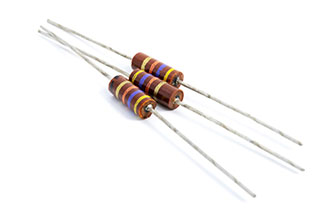
- Resistors: Used to limit current and divide voltage in circuits.
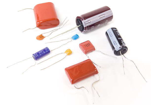
- Capacitors: Store and release electrical energy, available in electrolytic and ceramic types.
- Inductors: Store energy in a magnetic field, commonly used in filters and power supplies.

Image source: coilmaster.com
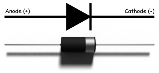
- Diodes: Allow current to flow in one direction, including rectifier and LED types.
- Transistors: Used for switching and amplification, such as BJTs and MOSFETs.
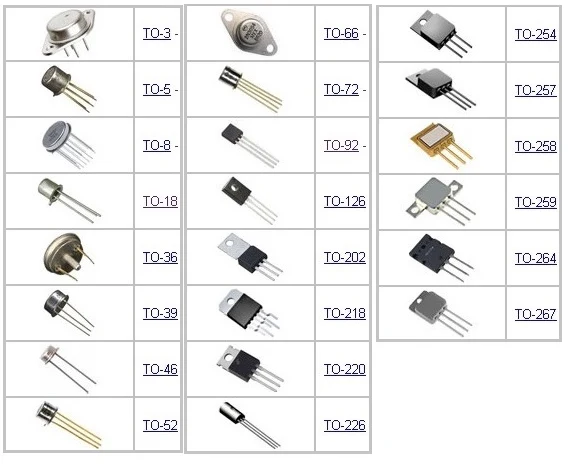
Image source: ElecTrade
- Integrated Circuits (ICs): Contain multiple electronic components in a single package.
 - 副本(1).png)
Image source: JY Electronics
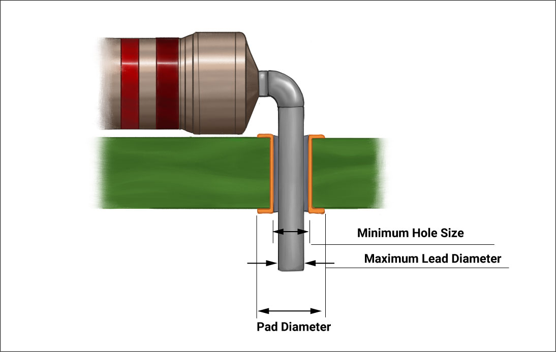
- Design Considerations: Ensure proper hole sizes and spacing for the component leads. Use plated through-holes for better electrical connectivity.
- Advantages:
- Stronger mechanical bond, making them suitable for high-stress environments.
- Easier to prototype and replace components during testing.
- Disadvantages:
- Require more space on the PCB, limiting design compactness.
- More labor-intensive to assemble, especially for mass production.
Surface-Mount Devices (SMD)
SMD components are mounted directly onto the surface of the PCB without the need for drilled holes. Here are some key points:
Types of SMD Components
- Resistors: Used to limit current and divide voltage in circuits. SMD resistors are typically rectangular and have a numerical code indicating their resistance value.
- Capacitors: Store and release electrical energy. SMD capacitors are available in ceramic, tantalum, and electrolytic types.
- Diodes: Allow current to flow in one direction, including rectifier and LED types. SMD diodes are small and often marked with a polarity indicator.
- Inductors: Store energy in a magnetic field, commonly used in filters and power supplies. SMD inductors are compact and come in various shapes, such as cylindrical or rectangular.
.webp)
Image source: MagTop
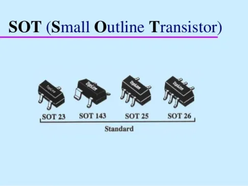
- Transistors: Used for switching and amplification, such as BJTs and MOSFETs. SMD transistors are compact and come in various packages like SOT-23 or SOT-223.
- Integrated Circuits (ICs): Contain multiple electronic components in a single package. SMD ICs are available in packages like QFP, SOIC, or BGA.
Sizes of SMD Components
SMD components are standardized in sizes, typically represented by a numerical code indicating their dimensions in hundredths of an inch. Common sizes include:
- Resistors and Capacitors: Sizes such as 0402 (0.04" x 0.02"), 0603 (0.06" x 0.03"), and 1206 (0.12" x 0.06"). Smaller sizes are used for compact designs, while larger sizes are easier to handle.
- Inductors: Sizes vary based on inductance and current ratings, with common sizes including 0805 and 1210.
- Diodes and Transistors: Sizes depend on the package type, such as SOT-23 or SOD-123 for diodes.
Codes for SMD Components
SMD components often use codes for identification due to their small size:
- Resistors: Use a three- or four-digit code to indicate resistance value (e.g., "103" for 10kΩ).
- Capacitors: Use numerical codes to indicate capacitance value and voltage rating (e.g., "104" for 100nF).
- Diodes: Use part numbers or polarity markings to identify type and orientation.
- Transistors: Use part numbers or package markings to identify type and specifications.
- Design Considerations: Ensure proper pad sizes and spacing for soldering. Use solder masks to prevent solder bridges.
- Advantages:
- Smaller size and lighter weight, allowing for compact and high-density designs.
- Automated assembly processes reduce labor costs and increase production speed.
- Disadvantages:
- More challenging to prototype and repair due to smaller sizes.
- Weaker mechanical bond compared to through-hole components.
Researching components and their packages is crucial for understanding electronic design in KiCad because it bridges the gap between theoretical circuit design and practical implementation. Each component package, such as through-hole or surface-mount, has a corresponding footprint in KiCad that defines its physical dimensions and pad layout on the PCB. By studying package codes and their associated footprints, I can ensure that the components I select will fit correctly on the board and be compatible with the manufacturing process. This knowledge also helps in assigning the right footprints during schematic design, avoiding errors during PCB layout and assembly. Understanding the relationship between package codes and footprints is essential for creating reliable and manufacturable designs.
Designing the Board
To design the board, I used KiCad, an open-source EDA tool. KiCad offers a comprehensive suite of features for PCB design, including schematic capture, PCB layout, 3D visualization, and Gerber file generation. I started by creating the schematic, where I placed and connected various components such as resistors, capacitors, and connectors. KiCad's extensive library of components and its ability to create custom components made this process straightforward. After completing the schematic, I switched to the PCB layout editor to arrange the components on the board and route the traces. KiCad's design rule checks (DRC) ensured that my layout met the necessary electrical and manufacturing constraints. Once the layout was finalized, I used the 3D viewer to inspect the board and verify the placement of components. Finally, I generated the Gerber files required for manufacturing. To produce the PCB, I opted for isolation milling, a process where a CNC machine removes the copper around the traces to create the circuit. This method is suitable for rapid prototyping and allowed me to quickly fabricate and test my development board.
Cloning the Fab Academy Components Library
Before starting the design process, I ensured that I used components available in the Fab Academy inventory by cloning the Fab Academy components library for KiCad. Below are the steps I followed:
-
Finding the Repository:
I navigated to the official Fab Academy GitLab repository for the KiCad components library. The repository can be found at the following link:
https://gitlab.fabcloud.org/pub/libraries/kicad
-
Cloning the Repository:
Using Visual Studio Code, I cloned the repository into a suitable folder in my documents. Below are the steps I followed:
First I followed the link above to the KiCad library and clicked on "Code" and then coppied the link under "Clone with HTTPS".
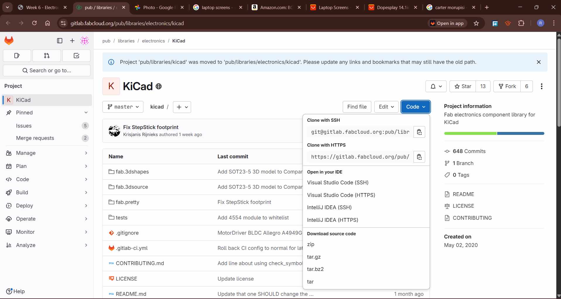
Coppying the HTTPS link.
- Opened Visual Studio Code and clicked on clone repository on the list.
- Clicked on Clone Repository and pasted the repository URL that i coppied above.
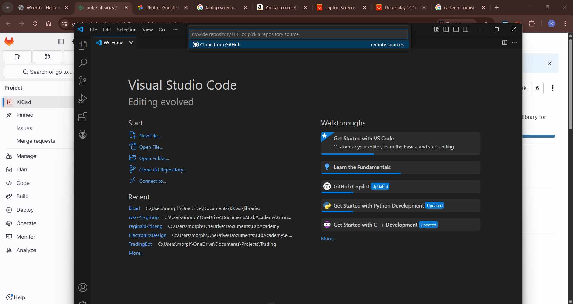
Opening new window on VS Code.
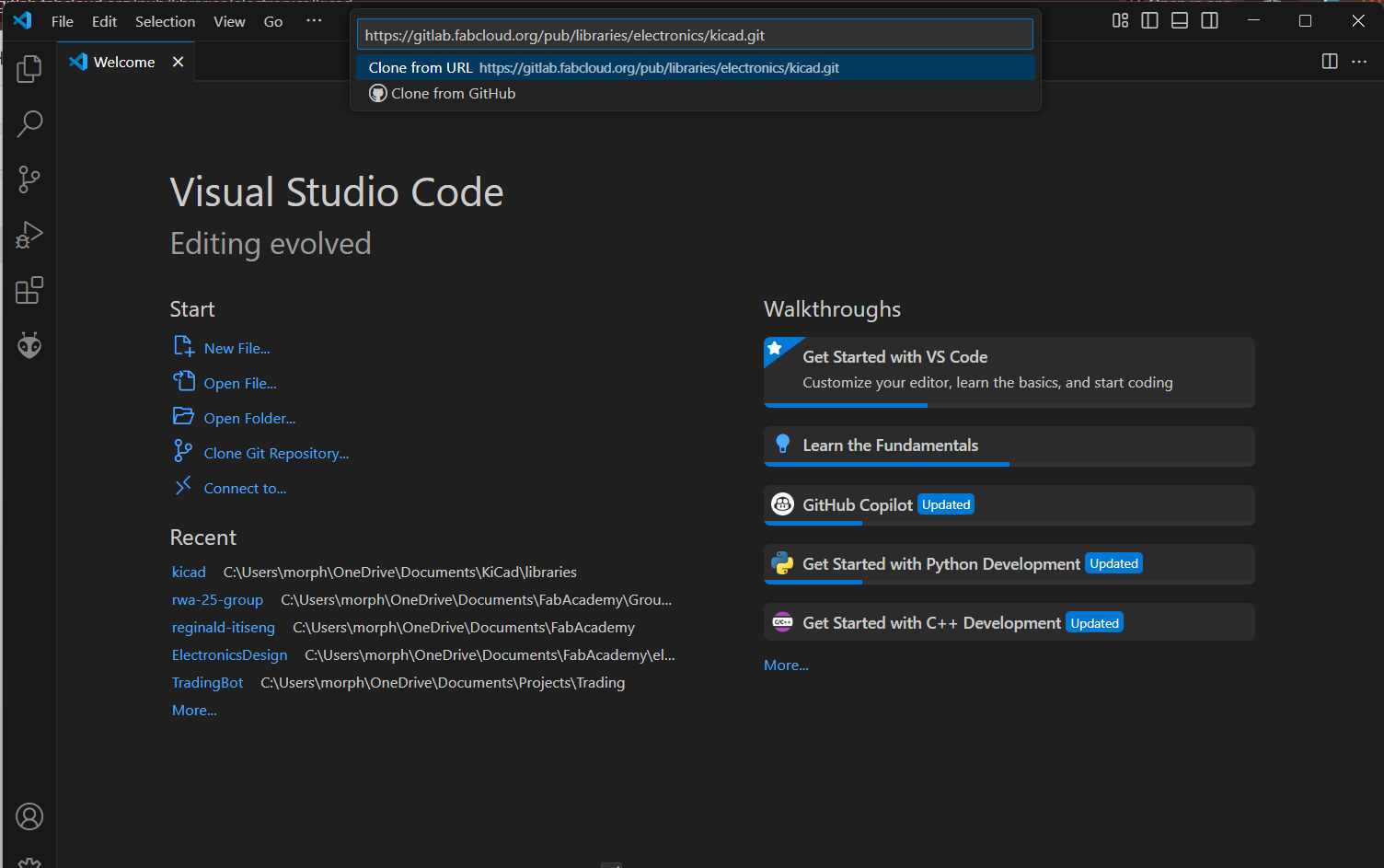
Pasting the Coppied Link on VS Code adn the hitting enter
- Selected a folder in my documents to store the cloned repository. For example:
C:/Users/morph/Documents/FabAcademy/KiCadLibraries.

The repo is now cloned and the image above shows the structure in the VS code file explorer.
-
Linking the Library in KiCad:
After cloning the repository, I linked the library in KiCad by following these steps:
- Opened KiCad and navigated to Preferences > Manage Symbol Libraries.

Addidng Symbol libararies
- Clicked on Add Existing Library and browsed to the cloned folder.
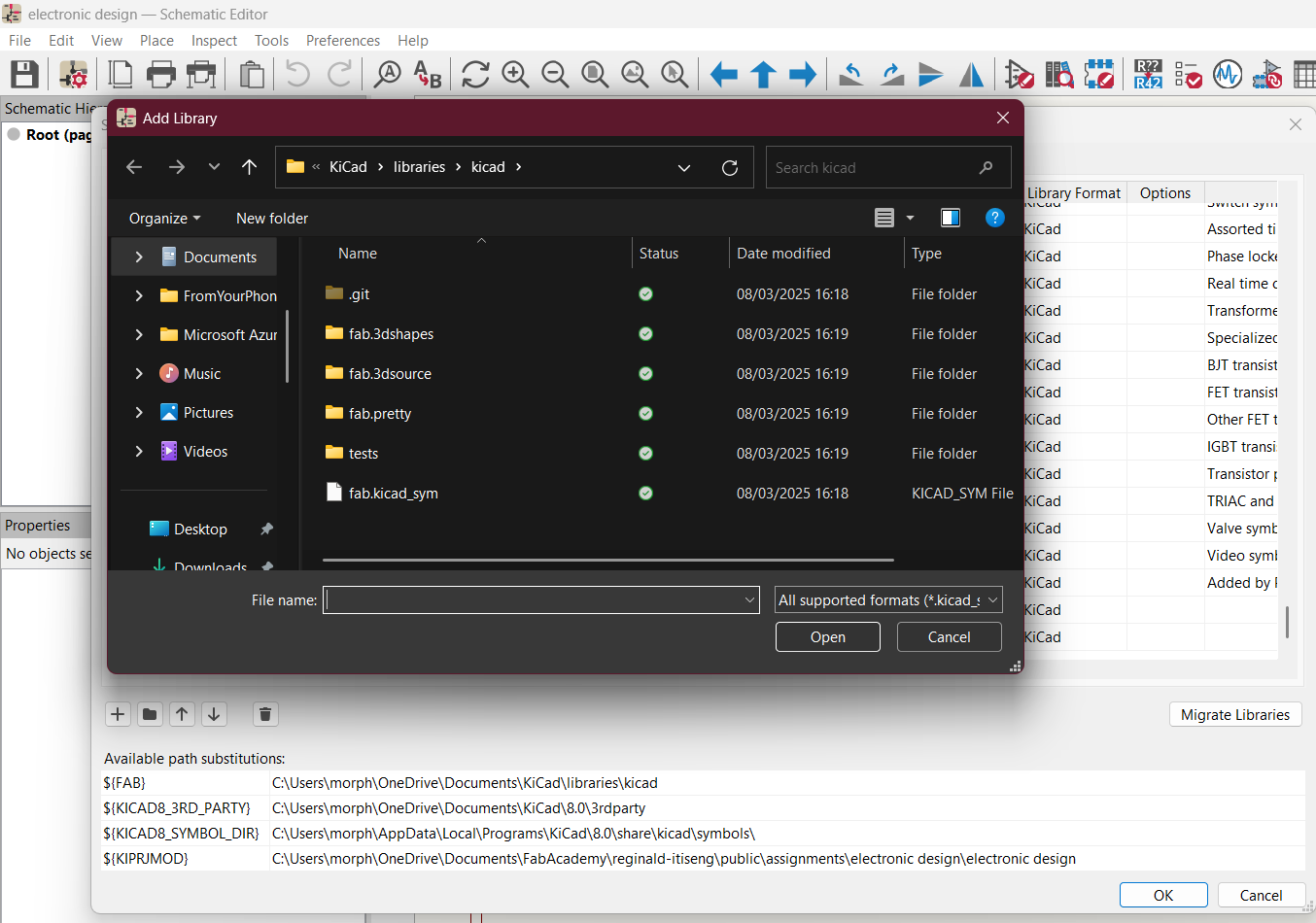
in the file explorer navigated to my cloned Fab Academy inventory repository location
- Selected the
fab.kicad_sym file from the cloned repository and added it to the global library list.
- Repeated the process for the footprint library by navigating to Preferences > Manage Footprint Libraries and adding the
fab.pretty folder.
-
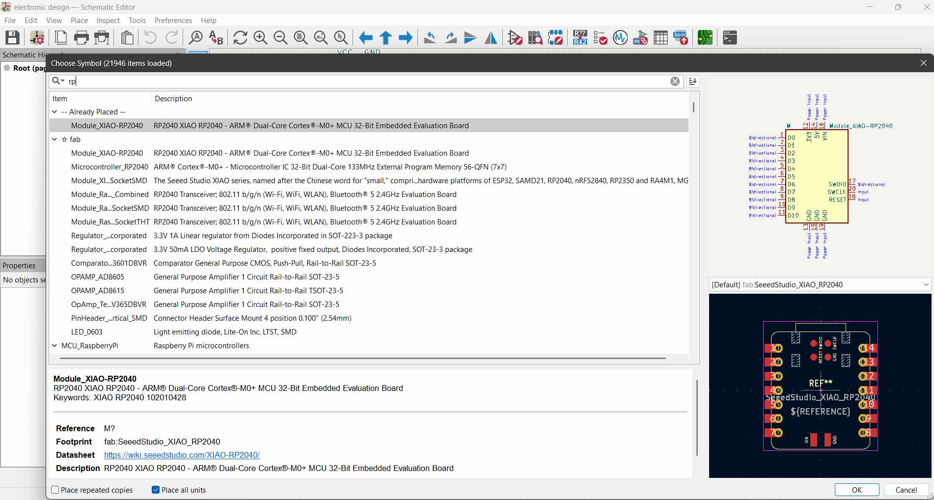
Verifying the Library:
To ensure the library was successfully linked, I opened the schematic editor in KiCad and searched for components from the Fab Academy library. The components were available and ready for use in my design.
By using the Fab Academy components library, I ensured that all components in my design were readily available in the inventory, simplifying the procurement and assembly process.
Component Selection and Soldering Considerations
For this project, I chose to use the Seeed Studio XIAO RP2040 microcontroller and 1206 size surface-mount device (SMD) components. The decision to use 1206 size components was based on the fact that I will be hand soldering the board. The larger size of 1206 components makes them easier to handle and solder compared to smaller SMD sizes, especially for beginners or when using basic soldering tools.
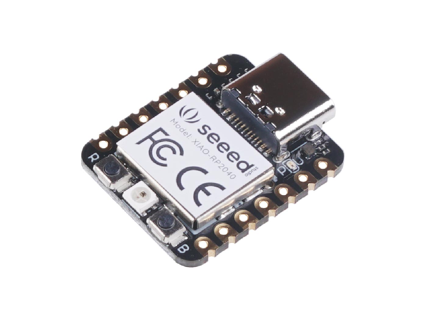
Image source: Seeed Studio
As part of the design, I included a resistor for the LED and another for the button. To determine the appropriate resistor values, I referred to the datasheets of the components and used Ohm's Law (V = IR) to calculate the resistance needed to limit the current through the LED and ensure proper operation of the button's pull-up configuration.
When reading the values of the resistors, I relied on the numerical codes printed on the SMD resistors. These codes typically consist of three or four digits. For example, a resistor marked "103" corresponds to 10 kΩ (10 followed by 3 zeros), while "472" corresponds to 4.7 kΩ. This coding system makes it easy to identify the resistance value without requiring additional tools.
Regarding polarity, resistors are non-polarized components, meaning they can be installed in either orientation on the PCB without affecting their functionality. This simplifies the assembly process, as there is no need to worry about aligning the resistor in a specific direction.
Below is a step-by-step guide of how I designed my development board using KiCad:
-
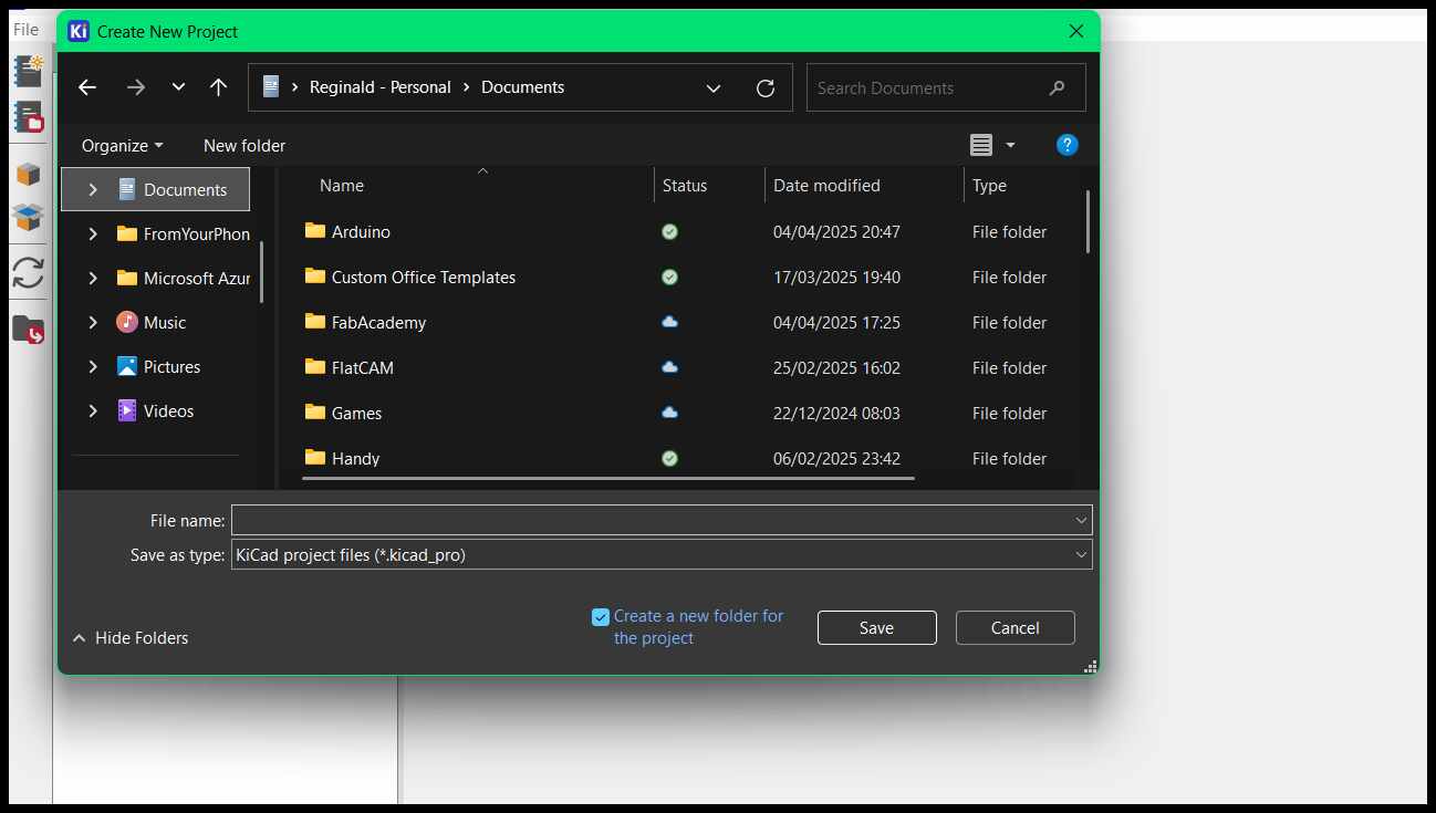
Setting Up the Project:
I started by creating a new project in KiCad and naming it appropriately. This created a folder containing the project files, including the schematic and PCB layout files.
-
Creating the Schematic:
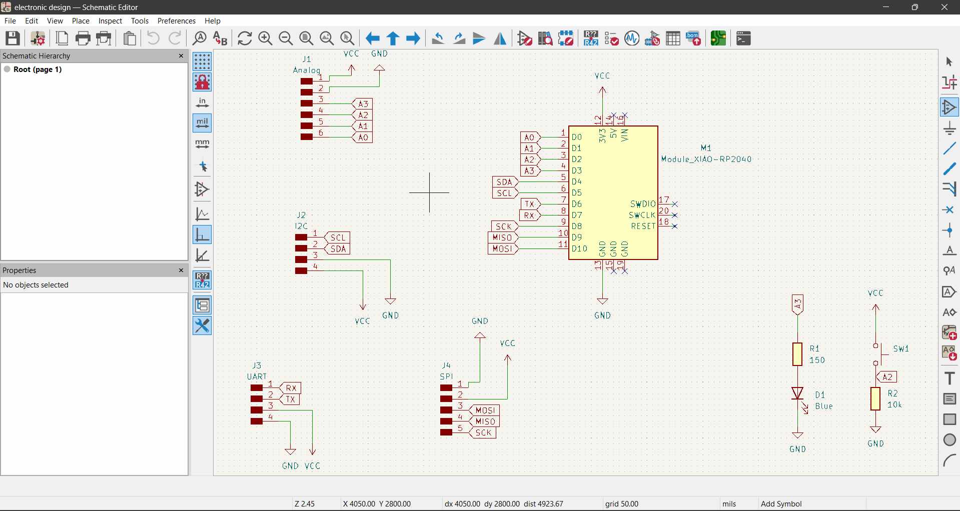
In the schematic editor, I added the Seeed Studio XIAO RP2040 microcontroller from the component library. I grouped the pins based on their functionality: UART, SPI, I2C, and general GPIO pins. This organization made it easier to plan the connections.
I then added a button and an LED to the schematic. The button was connected to a GPIO pin with a pull-down resistor, and the LED was connected to another GPIO pin through a current-limiting resistor. I ensured that all components were surface-mount devices (SMD) to keep the design compact.
I used components that were already available in the Fab Accademy inventory.
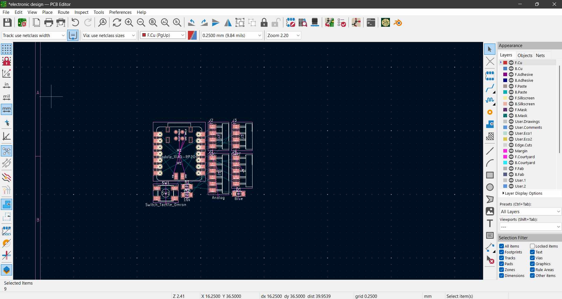
The image bellow shows the complete circuit with the pin headers connected through net labels. the grouping of the different microcontroller interfaces can already been seen here.
-
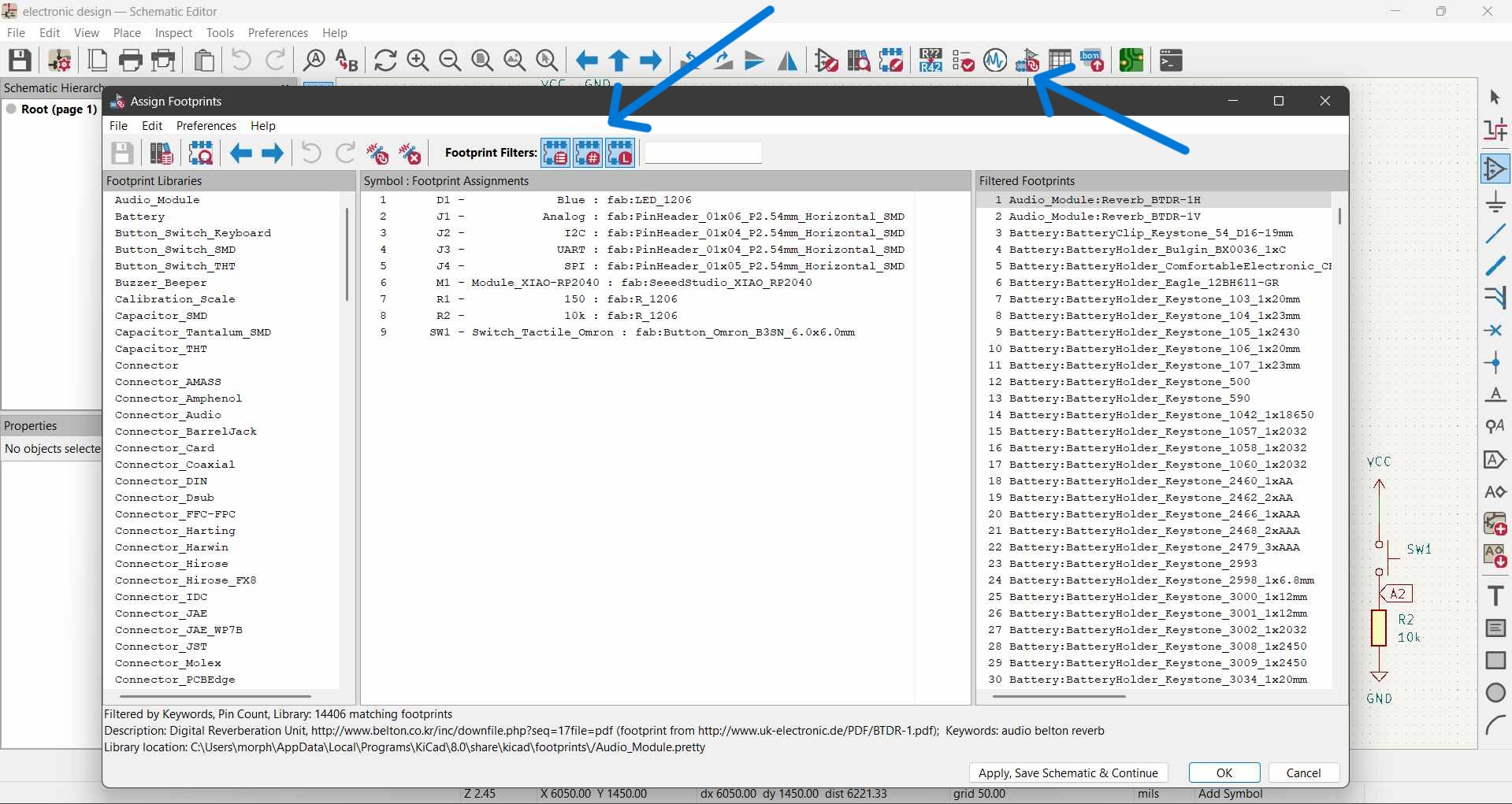
Assigning Footprints:
After completing the schematic, I assigned appropriate SMD footprints to each component. For example, I used 0603 footprints for resistors and capacitors, and the XIAO RP2040 footprint for the microcontroller.
-
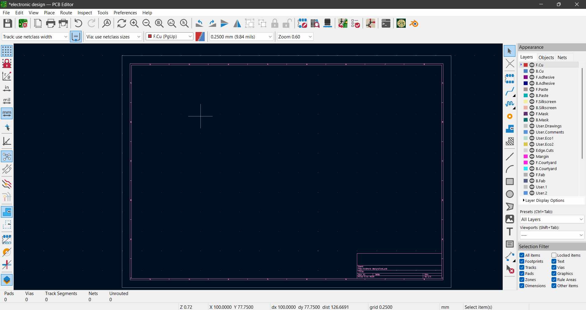
Designing the PCB Layout:
In the PCB layout editor, I imported the schematic and arranged the components on the board. I placed the XIAO RP2040 at the center and grouped the related components (e.g., resistors, capacitors, button, and LED) around it for logical placement.
I routed the traces, ensuring that the power and ground lines were wide enough to handle the current. I also added a ground plane to reduce noise and improve signal integrity.
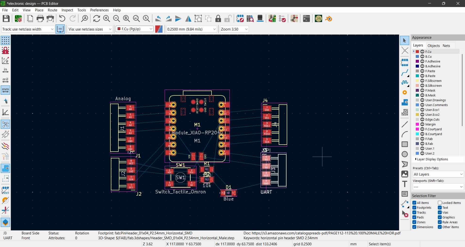
The image above shows the view i get after clicking on "Switch to PCB editor" button on the Schematic editor window.
On the pcb editor window I click on "Update PCB from scematic" which loaded up the components with their footprints, as seen above.
With the components loaded, I began placing the components optimally around the microcontroller.
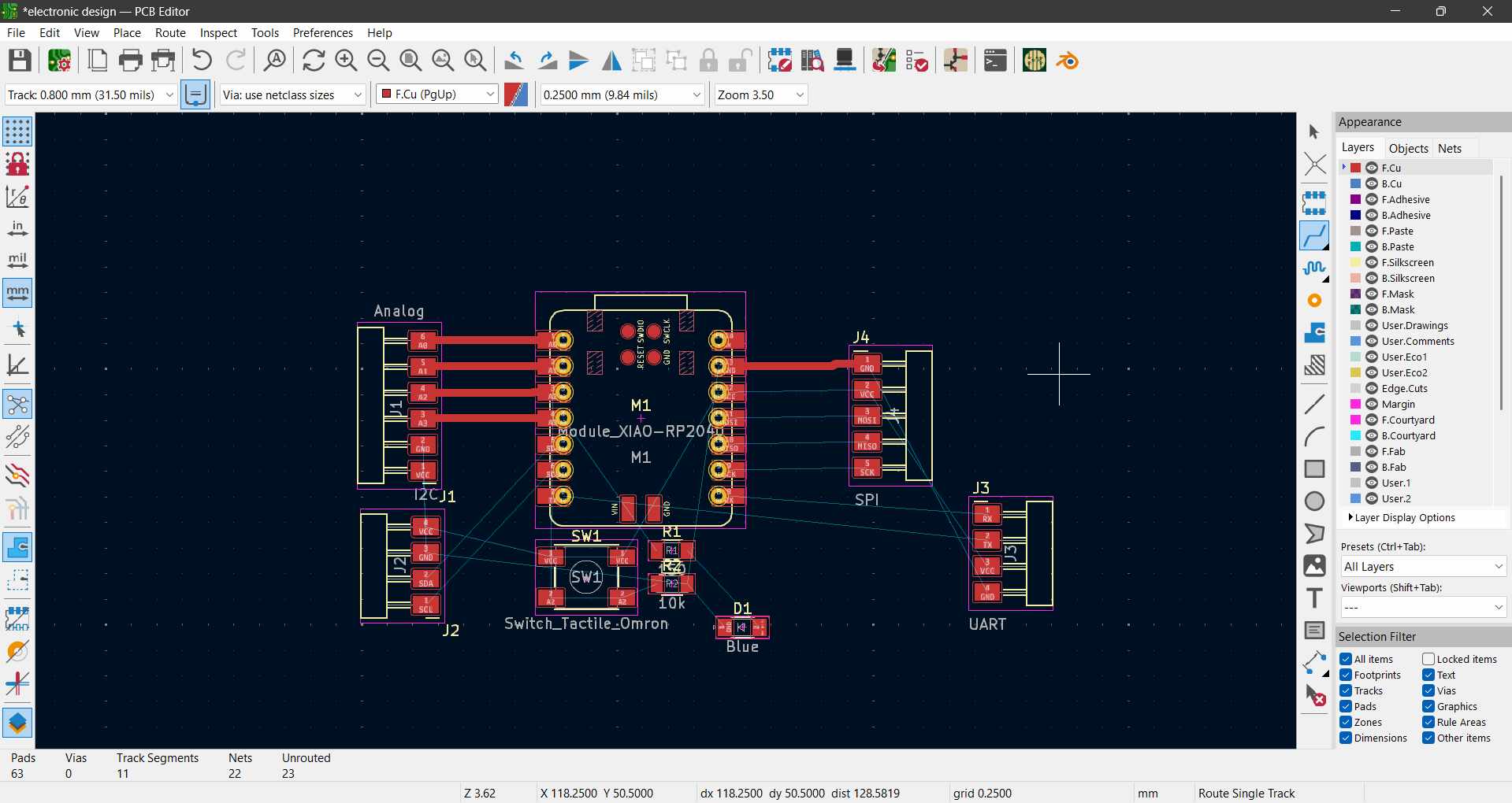
After placing components I began routing with 0.8mm traces.
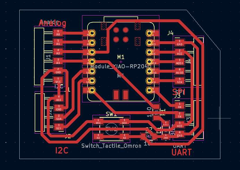
This images shows the complete baord routing done, all traces at 0.8mm.
-
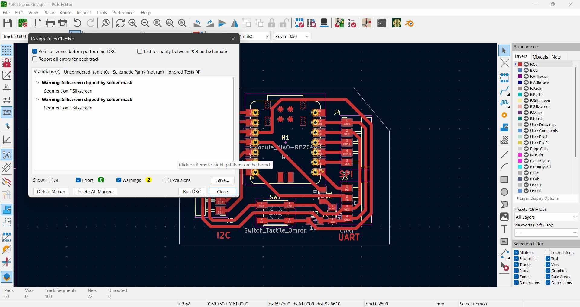
Design Rule Checks (DRC):
Once the layout was complete, I ran the design rule checks (DRC) to ensure there were no errors, such as overlapping traces or unconnected nets. I resolved any issues flagged by the DRC tool.
-
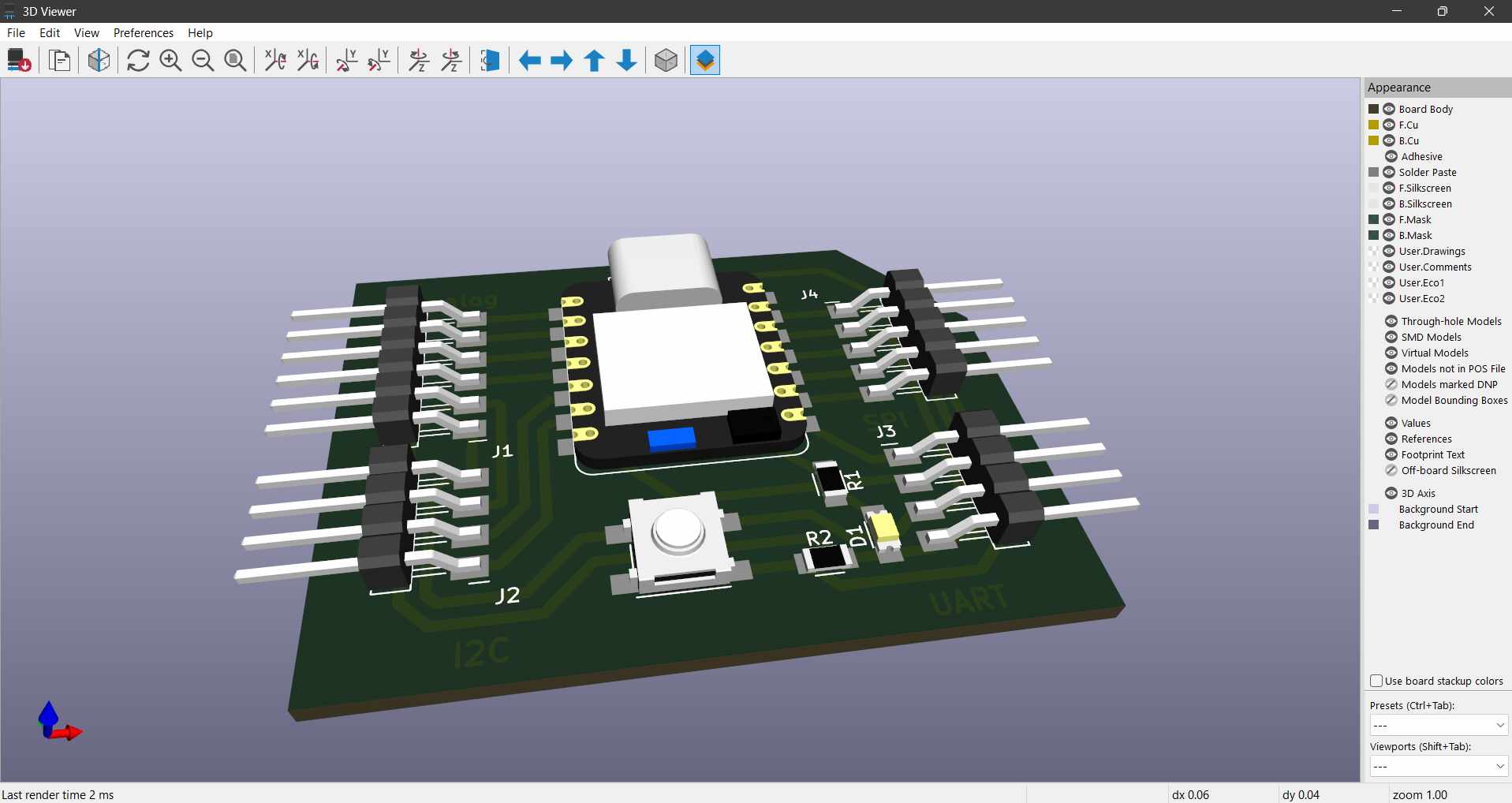
3D Visualization:
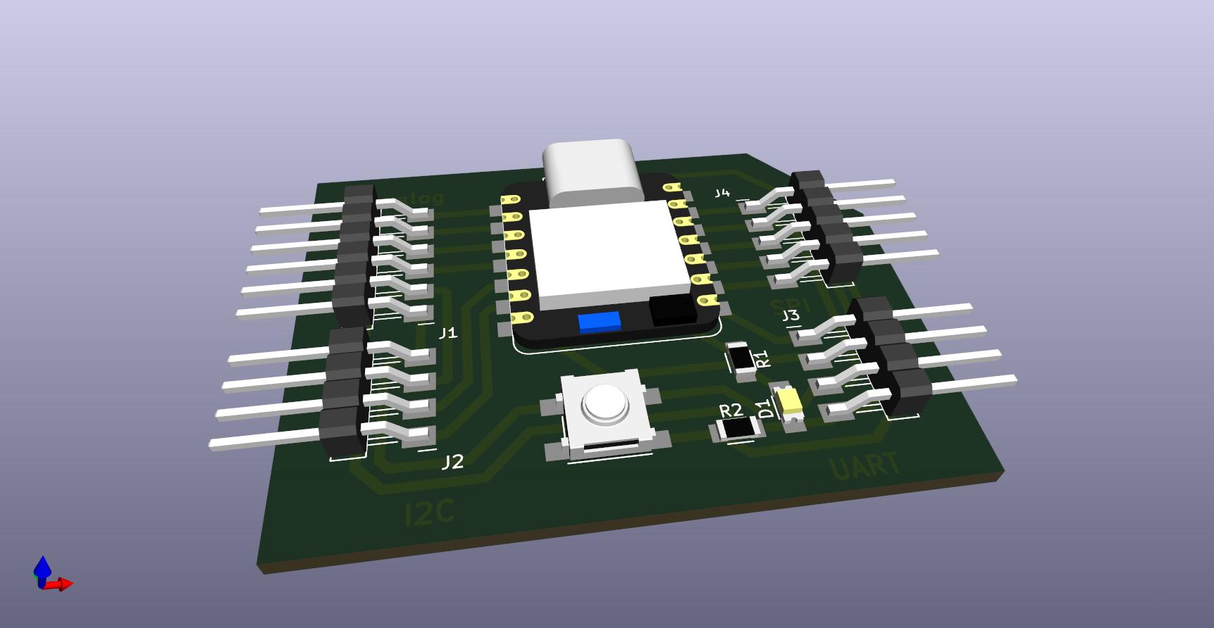
Using KiCad's 3D viewer, I inspected the board to verify the placement of components and ensure there were no mechanical conflicts. This step helped me visualize the final design before manufacturing.
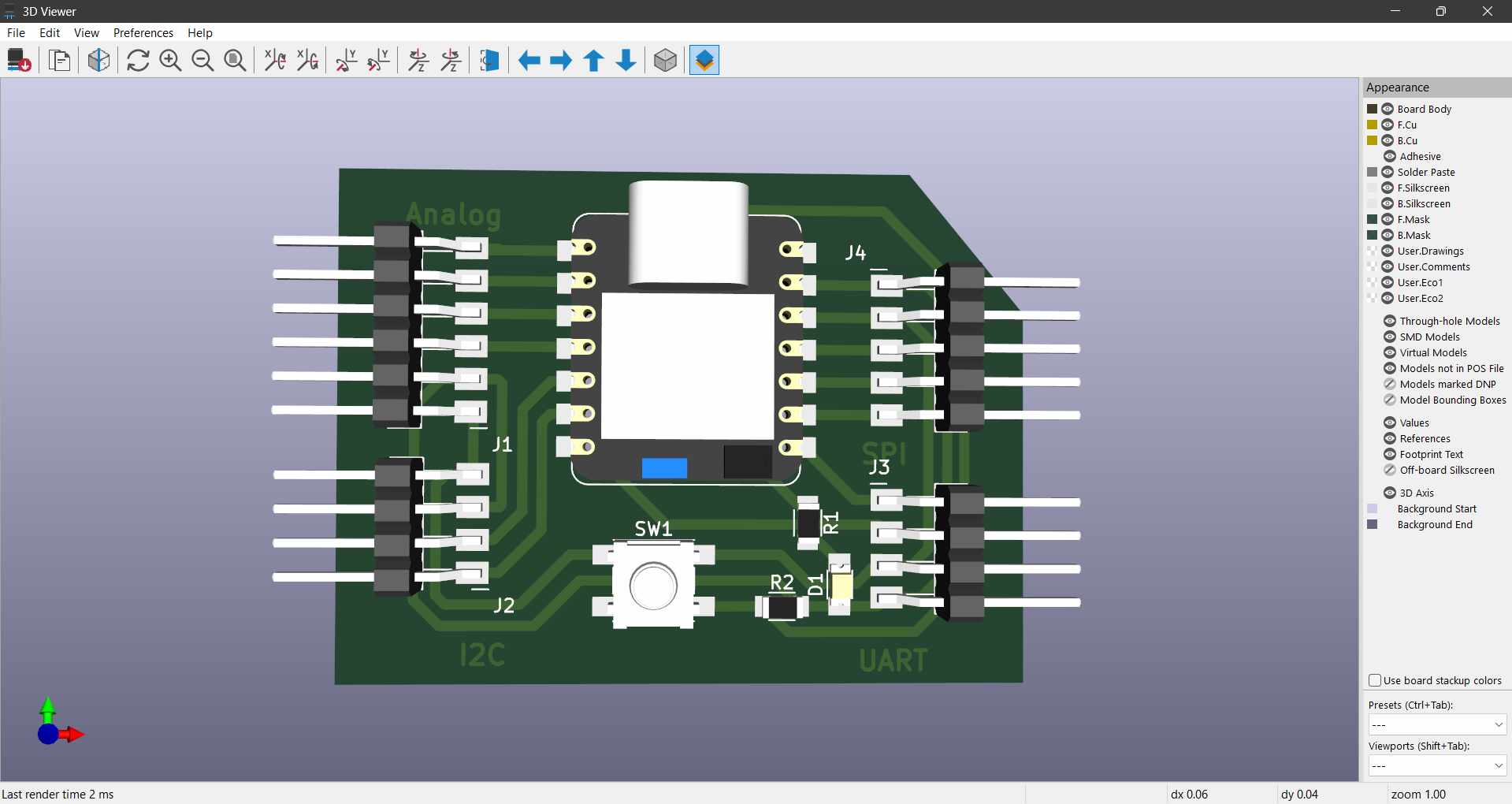
The complete Board can be seen here and matches exactly what i planned for.
The final design was compact and optimized for surface-mount components, making it suitable for modern manufacturing processes. The board included all the necessary features, such as grouped pins, a button, and an LED, to support the functionality of the Seeed Studio XIAO RP2040 microcontroller.
Design Files
Below are the design files for my development board:
Download Zip
Hero-Shot
Below is the hero-shot of my development board: